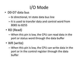
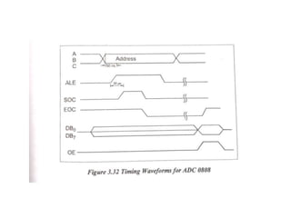
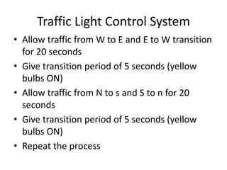
UNIT 3
PROGRAMMABLE PERIPERAL
INTERFACE
Content
• Introduction
• Architecture of 8255
• Keyboard interfacing
• LED display –interfacing
• ADC and DAC interface
• Temperature Control
• Stepper Motor Control
• Traffic Control interface
Introduction
• To communicate with the outside world,
microprocessor use peripherals (I/O devices)
• Input devices – Keyboards, A/D converters
etc.,
• Output devices – CRT, Printers, LEDs etc.,
• Peripherals are connected to the
microprocessors through electronic circuit
known as interfacing circuits.
Microprocessors unit with I/O devices
Input
devices
(keyboard)
Micro
processors
Output
devices
(LED)
Input
peripherals
Output
peripherals
• Some of the general purpose interfacing devices
– I/O ports
– Programmable peripherals interface (PPI)
– DMA controllers
– Interrupt controller
• Some of the special purpose interfacing devices
– CRT controller
– Keyboard
– Display
– Floppy Disc controllers
Peripheral interfacing Chips are used
generation of I/O ports
• Programmable peripherals interface Inter 8255 (PPI)
• Programmable Interrupt controller (PIC) Intel 8259
• Programmable communication interface (PCI) Intel
8251
• Keyboard display Controller Intel 8279
• Programmable counter /Inverter timer Intel 8253
• A/D and D/A Converter Interfacing
Microprocessors unit with I/O devices
Input
devices
(key
board)
PPI
8255
Micro
proce
ssors
8279
Display
Output
device
(LED)
Peripheral
Interface
Display
Interface
Address Space Partitioning
• The Microprocessors uses 16 bit wide address
bus for addressing memories and I/O devices.
• Using 16 bit wide address bus, it can access
216 = 64k bytes of memory and I/O devices
• Two schemes for the allocation of addresses
to memories and I/O devices
– Memory mapped I/O
– I/O mapped I/O
Memory mapped I/O
• It has only one address space
• Address space is defined as the set of all possible
addresses that a microprocessor can generate
• Some addresses assigned to memories and Some
addresses to I/O devices
• Memory locations are assigned with addresses
from 8000 to 84FF
• I/O devices are assigned with addresses from
8500 to 85FF
I/O mapped I/O scheme
• In this scheme, addresses assigned to
memories locations can also be assigned to
I/O devices
• Since the same address may be assigned to
memories locations or an I/O devices
• The microprocessor has a signal to distinguish
whether the address on the address bus is for
memories locations or an I/O devices
I/O mapped I/O scheme
• When signal is high, then address on the address bus is
for an I/O devices
• When signal is low, then address on the address bus is
for memory locations
• Two extra instruction IN and OUT are used to address
I/O devices.
• The IN instruction is used to read the data of an input
devices.
• The OUT instruction is used to send the data of an
input devices.
• This scheme is suitable for a large system.
PROGRAMMABLE PERIPHERALS INTERFACE INTER 8255
(PPI)
Operating mode of 8255
• Bit Set Reset (BSR) Mode
• I/O Mode
Bit Set Reset (BSR) Mode
BSR control word format
I/O Mode
• The 8255 has the following 3 modes of
operation
– Mode 0 – Simple Input/output
– Mode 1 – Input / Output with the Handshake or
strobed
– Mode 2 – Bi-directional I/O
I/O Mode
Mode 0 – Simple Input/output
– Port A and port B are used as two simple 8-bit I/O
port
– Port C as two 4-bit port
• Features
– Outputs are latched
– Inputs are buffered not latched
– Ports do not have handshake or interrupt
capability
I/O Mode
• Mode 1 – Input / Output with the Handshake
– Input or output data transfer is controlled by
handshaking signals.
– Handshaking signals are used to transfer data
between devices whose data transfer speeds are
not same.
– Port A and Port B are designed to operate with the
Port C.
– When Port A and Port B are programmed in Mode
1, 6 pins of port C is used for their control.
I/O Mode
• D0-D7 data bus
– bi directional, tri state data bus line
– It is used to transfer data and control word from
8085 to 8255
• RD (Read)
– When this pin is low, the CPU can read data in the
port or status word through the data buffer
• WR (write)
– When this pin is low, the CPU can write data in the
port or in the control register through the data
buffer
I/O Mode
• Mode 2 – Bi-directional I/O
• Port A can be programmed to operate as a
bidirectional port.
• The mode 2 operation is only for port A
• When port A is programmed in Mode 2, the
Port B can be used in either Mode 1 or Mode
0.
• Mode 2 operation the port a is controlled by
PC3 to PC7 of port C.
PIN
DIAGRAM
OF 8255
PROGRAMMING and OPERATION of
8255
• Programming in MODE 0
• D7 –set to 1
• D6,D5,D2- all set to 0 –MODE 0
• D4,D3,D1 and D0- determine weather the
corresponding ports are to configured as input
or output
A B GROUP A GROUP B
D4 D3 D1 D0 PORT A PORTC U PORT B PORT C L
0 0 0 0 OUT OUT OUT OUT
0 0 0 1 OUT OUT OUT IP
0 0 1 0 OUT OUT IP OUT
0 0 1 1 OUT OUT IP IP
0 1 0 0 OUT IP OUT OUT
0 1 0 1 OUT IP OUT IP
0 1 1 0 OUT IP IP OUT
0 1 1 1 OUT IP IP IP
1 0 0 0 IP OUT OUT OUT
1 0 0 1 IP OUT OUT IP
1 0 1 0 IP OUT IP OUT
1 0 1 1 IP OUT IP IP
1 1 0 0 IP IP OUT OUT
1 1 0 1 IP IP OUT IP
1 1 1 0 IP IP IP OUT
1 1 1 1 IP IP IP IP
Programming in MODE 1
• IBF- input buffer full
• INTR- interrupt request
• INTE-interrupt enable
• OBF-output buffer full
• INTR-interrupt request
• INTE-interrupt enable
Programming in MODE 2
Interfacing cable
Basic Key operation
2 X 2 Key operation
Keyboard Microprocessor Interface software Flowchart
INTERFACING-keyboard
LED Operation
Microprocessor interface to LED
(Common anode)
Microprocessor interface to 7 segment LED
(Parallel)
Microprocessor interface to 7
segment LED (serial)
Serial interface of 7
segment LED to
Microprocessor
software flowchart
INTERFACE-LED display
ADC INTERFACE
BLOCK diagram of ADC 0808
PIN diagram of ADC 0808
DAC INTERFACE
Pin diagram of DAC
Pin diagram of DAC
INTERFACING diagram for DAC
TEMPERATURE CONTROL
• Temperature sensor –convert temp to
electrical signal by thermistor
• Transducer convert physical data into
electrical signal
• Physical data –temp, light, flow, speed etc…
• LM34 & LM35 –temperature sensor by
NATIONAL SEMICONDUCTOR CO-OPERATION
• LM34
• Output voltage is
linearly proportional to
Fahrenheit temp
• No external calibration
• 10mV for each degree
of Fahrenheit temp
• LM35
• Output voltage is
linearly proportional to
Celsius temp
• No external calibration
• 10mV for each degree
of Centigrate temp
STEPPER MOTOR CONTROL interface
• Digital motor used to translate electrical pulse
into mechanical movement
• Center tap winding connected to 12 V supply
• Motor can be excited by grounding four
terminals of the two windings
• ROTOR-Stepper motor has permanent magnet
rotor .It is also known as shaft
• STEP ANGLE-It is minimum degree of rotation
associated with a single step
Stepper Motor Interface
Excitation Table
Step X1 X2 X3 X4
1 0 1 0 1
2 1 0 0 1
3 1 0 1 0
4 0 1 1 0
1 0 1 0 1
Traffic Light Control System
• Allow traffic from W to E and E to W transition
for 20 seconds
• Give transition period of 5 seconds (yellow
bulbs ON)
• Allow traffic from N to s and S to n for 20
seconds
• Give transition period of 5 seconds (yellow
bulbs ON)
• Repeat the process
Traffic Light Control System
Interfacing diagram for Traffic Light
Control System
Unit 3-PROGRAMMABLE PERIPHERAL INTERFACE-ME6702– MECHATRONICS

Unit 3-PROGRAMMABLE PERIPHERAL INTERFACE-ME6702– MECHATRONICS

  • 1.
  • 2.
    Content • Introduction • Architectureof 8255 • Keyboard interfacing • LED display –interfacing • ADC and DAC interface • Temperature Control • Stepper Motor Control • Traffic Control interface
  • 3.
    Introduction • To communicatewith the outside world, microprocessor use peripherals (I/O devices) • Input devices – Keyboards, A/D converters etc., • Output devices – CRT, Printers, LEDs etc., • Peripherals are connected to the microprocessors through electronic circuit known as interfacing circuits.
  • 4.
    Microprocessors unit withI/O devices Input devices (keyboard) Micro processors Output devices (LED) Input peripherals Output peripherals
  • 5.
    • Some ofthe general purpose interfacing devices – I/O ports – Programmable peripherals interface (PPI) – DMA controllers – Interrupt controller • Some of the special purpose interfacing devices – CRT controller – Keyboard – Display – Floppy Disc controllers
  • 6.
    Peripheral interfacing Chipsare used generation of I/O ports • Programmable peripherals interface Inter 8255 (PPI) • Programmable Interrupt controller (PIC) Intel 8259 • Programmable communication interface (PCI) Intel 8251 • Keyboard display Controller Intel 8279 • Programmable counter /Inverter timer Intel 8253 • A/D and D/A Converter Interfacing
  • 7.
    Microprocessors unit withI/O devices Input devices (key board) PPI 8255 Micro proce ssors 8279 Display Output device (LED) Peripheral Interface Display Interface
  • 8.
    Address Space Partitioning •The Microprocessors uses 16 bit wide address bus for addressing memories and I/O devices. • Using 16 bit wide address bus, it can access 216 = 64k bytes of memory and I/O devices • Two schemes for the allocation of addresses to memories and I/O devices – Memory mapped I/O – I/O mapped I/O
  • 9.
    Memory mapped I/O •It has only one address space • Address space is defined as the set of all possible addresses that a microprocessor can generate • Some addresses assigned to memories and Some addresses to I/O devices • Memory locations are assigned with addresses from 8000 to 84FF • I/O devices are assigned with addresses from 8500 to 85FF
  • 10.
    I/O mapped I/Oscheme • In this scheme, addresses assigned to memories locations can also be assigned to I/O devices • Since the same address may be assigned to memories locations or an I/O devices • The microprocessor has a signal to distinguish whether the address on the address bus is for memories locations or an I/O devices
  • 11.
    I/O mapped I/Oscheme • When signal is high, then address on the address bus is for an I/O devices • When signal is low, then address on the address bus is for memory locations • Two extra instruction IN and OUT are used to address I/O devices. • The IN instruction is used to read the data of an input devices. • The OUT instruction is used to send the data of an input devices. • This scheme is suitable for a large system.
  • 12.
  • 13.
    Operating mode of8255 • Bit Set Reset (BSR) Mode • I/O Mode
  • 14.
    Bit Set Reset(BSR) Mode BSR control word format
  • 15.
    I/O Mode • The8255 has the following 3 modes of operation – Mode 0 – Simple Input/output – Mode 1 – Input / Output with the Handshake or strobed – Mode 2 – Bi-directional I/O
  • 16.
    I/O Mode Mode 0– Simple Input/output – Port A and port B are used as two simple 8-bit I/O port – Port C as two 4-bit port • Features – Outputs are latched – Inputs are buffered not latched – Ports do not have handshake or interrupt capability
  • 17.
    I/O Mode • Mode1 – Input / Output with the Handshake – Input or output data transfer is controlled by handshaking signals. – Handshaking signals are used to transfer data between devices whose data transfer speeds are not same. – Port A and Port B are designed to operate with the Port C. – When Port A and Port B are programmed in Mode 1, 6 pins of port C is used for their control.
  • 18.
    I/O Mode • D0-D7data bus – bi directional, tri state data bus line – It is used to transfer data and control word from 8085 to 8255 • RD (Read) – When this pin is low, the CPU can read data in the port or status word through the data buffer • WR (write) – When this pin is low, the CPU can write data in the port or in the control register through the data buffer
  • 19.
    I/O Mode • Mode2 – Bi-directional I/O • Port A can be programmed to operate as a bidirectional port. • The mode 2 operation is only for port A • When port A is programmed in Mode 2, the Port B can be used in either Mode 1 or Mode 0. • Mode 2 operation the port a is controlled by PC3 to PC7 of port C.
  • 20.
  • 22.
    PROGRAMMING and OPERATIONof 8255 • Programming in MODE 0 • D7 –set to 1 • D6,D5,D2- all set to 0 –MODE 0 • D4,D3,D1 and D0- determine weather the corresponding ports are to configured as input or output
  • 23.
    A B GROUPA GROUP B D4 D3 D1 D0 PORT A PORTC U PORT B PORT C L 0 0 0 0 OUT OUT OUT OUT 0 0 0 1 OUT OUT OUT IP 0 0 1 0 OUT OUT IP OUT 0 0 1 1 OUT OUT IP IP 0 1 0 0 OUT IP OUT OUT 0 1 0 1 OUT IP OUT IP 0 1 1 0 OUT IP IP OUT 0 1 1 1 OUT IP IP IP 1 0 0 0 IP OUT OUT OUT 1 0 0 1 IP OUT OUT IP 1 0 1 0 IP OUT IP OUT 1 0 1 1 IP OUT IP IP 1 1 0 0 IP IP OUT OUT 1 1 0 1 IP IP OUT IP 1 1 1 0 IP IP IP OUT 1 1 1 1 IP IP IP IP
  • 24.
  • 25.
    • IBF- inputbuffer full • INTR- interrupt request • INTE-interrupt enable • OBF-output buffer full • INTR-interrupt request • INTE-interrupt enable
  • 26.
  • 28.
  • 29.
  • 31.
    2 X 2Key operation
  • 32.
  • 33.
  • 36.
  • 38.
    Microprocessor interface toLED (Common anode)
  • 40.
    Microprocessor interface to7 segment LED (Parallel)
  • 41.
    Microprocessor interface to7 segment LED (serial)
  • 42.
    Serial interface of7 segment LED to Microprocessor software flowchart
  • 43.
  • 45.
  • 46.
  • 48.
  • 49.
  • 50.
  • 51.
  • 52.
  • 53.
    TEMPERATURE CONTROL • Temperaturesensor –convert temp to electrical signal by thermistor • Transducer convert physical data into electrical signal • Physical data –temp, light, flow, speed etc… • LM34 & LM35 –temperature sensor by NATIONAL SEMICONDUCTOR CO-OPERATION
  • 54.
    • LM34 • Outputvoltage is linearly proportional to Fahrenheit temp • No external calibration • 10mV for each degree of Fahrenheit temp • LM35 • Output voltage is linearly proportional to Celsius temp • No external calibration • 10mV for each degree of Centigrate temp
  • 56.
    STEPPER MOTOR CONTROLinterface • Digital motor used to translate electrical pulse into mechanical movement • Center tap winding connected to 12 V supply • Motor can be excited by grounding four terminals of the two windings • ROTOR-Stepper motor has permanent magnet rotor .It is also known as shaft • STEP ANGLE-It is minimum degree of rotation associated with a single step
  • 58.
  • 59.
    Excitation Table Step X1X2 X3 X4 1 0 1 0 1 2 1 0 0 1 3 1 0 1 0 4 0 1 1 0 1 0 1 0 1
  • 60.
    Traffic Light ControlSystem • Allow traffic from W to E and E to W transition for 20 seconds • Give transition period of 5 seconds (yellow bulbs ON) • Allow traffic from N to s and S to n for 20 seconds • Give transition period of 5 seconds (yellow bulbs ON) • Repeat the process
  • 61.
  • 62.
    Interfacing diagram forTraffic Light Control System