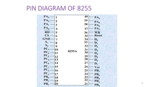
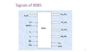
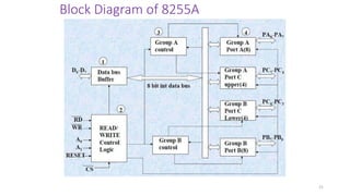
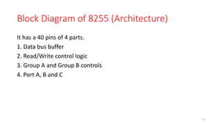
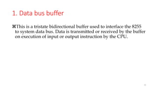
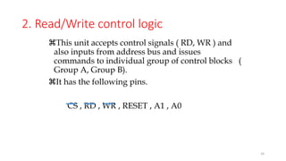
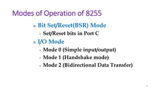
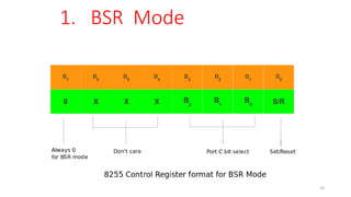
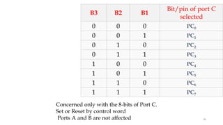
The document discusses peripheral interfacing with various ICs like 8255, 8259, 8254, 8279, and A/D and D/A converters. It provides details about the architecture, configuration, and interfacing of these ICs with 8085 and 8051 microprocessors. Specifically, it describes the 8255 PPI chip, its pin diagram, block diagram, modes of operation including bit set/reset mode and I/O modes 0, 1, and 2. It also discusses memory mapped I/O versus I/O mapped I/O and synchronous versus asynchronous data transfers.

![UNIT 4 Syllabus
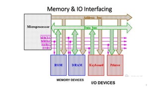
Introduction: Memory Interfacing & I/O interfacing
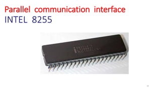
• 8255 PPI {Parallel communication interface}
• 8259 {Programmable Interrupt controller }
• 8253/8254 Timer {Timer or counter}
• 8237/8257 {DMA controller}
• 8251 USART {Serial communication interface}
• 8279 {Keyboard /display controller}
• A/D and D/A Interface {ADC 0800/0809,DAC 0800}
[Interfacing with 8085 & 8051]](https://image.slidesharecdn.com/unit-iv-221110133153-af845783/85/Unit-IV-pptx-3-320.jpg)