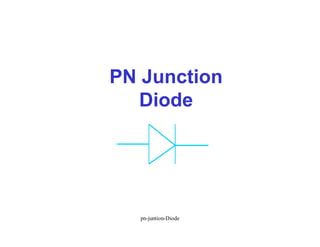
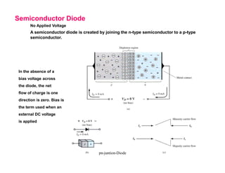
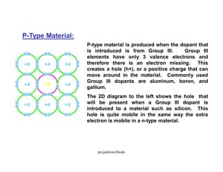
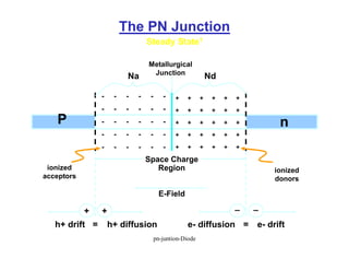
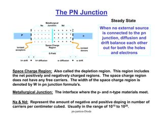
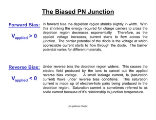
A p-n junction diode consists of a p-type semiconductor joined to an n-type semiconductor. When the two materials are joined, charge carriers diffuse across the junction leaving a depletion region devoid of free carriers. This creates a built-in electric field.
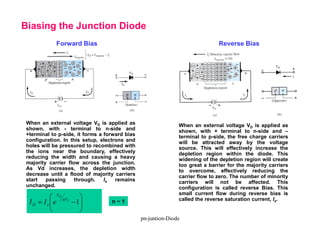
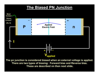
When a p-n junction diode is forward biased, the depletion region narrows allowing majority carriers to flow more easily across the junction. When reverse biased, the depletion region widens blocking the flow of majority carriers and only allowing a small leakage current of minority carriers.
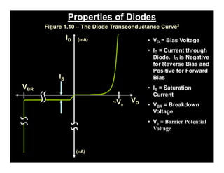
P-n junction diodes have applications as rectifiers, solar cells, LEDs, and are components of other semiconductor devices like transistors. The behavior of diodes is modeled by the
1) A pn junction diode consists of a p-type semiconductor joined to an n-type semiconductor. When the two materials come together, electrons from the n-type region combine with holes from the p-type region, leaving an uncharged depletion region.
2) When a forward bias is applied, the depletion region narrows, lowering the barrier for majority carriers to flow across the junction. Under reverse bias, the depletion region widens, blocking most carrier flow.
3) Diodes are commonly made from silicon or germanium as the base semiconductor material. Doping one region with elements from group III makes it p-type, while doping the other with elements from group V makes it n-type
The document discusses diodes and p-n junctions. It begins with an introduction and outline then covers:
- Formation of p-n junctions through doping of n-type and p-type semiconductors.
- Energy band diagrams which show band structure changes at junction.
- Concepts of built-in potential and how diffusion generates an electric field and potential barrier.
- Forward and reverse bias modes, and how applied voltage affects carrier concentrations and barrier.
- Derivation of the diode I-V characteristic equation from diffusion equations.
- Linear piecewise models approximate the diode as a battery and resistor in series.
- Breakdown diodes operate
This document provides information about PN junction diodes and their characteristics:
1) It describes how a PN junction is formed by combining P-type and N-type semiconductors, forming a depletion region.
2) It explains the I-V characteristics of a diode under forward and reverse bias, including how the depletion region changes with bias.
3) Additional topics covered include drift and diffusion currents, temperature effects, capacitance effects, and recovery time characteristics important for switching applications. Special diodes like Zener diodes are also introduced.
Minor project report on pn junction, zener diode, led characteristicsom prakash bishnoi
This document provides an overview of PN junction diodes, including their construction, operating principles, and I-V characteristics under forward and reverse bias conditions. In forward bias, the depletion region narrows allowing electrons and holes to flow across the junction, resulting in a lower resistance path. In reverse bias, the depletion region widens inhibiting flow and resulting in a very small saturation current until breakdown. The document explains the diffusion, drift, and recombination processes that occur under equilibrium and biasing conditions.
The document discusses P-N junctions, which are formed at the interface between P-type and N-type semiconductors. When these materials come into contact, majority charge carriers diffuse across the junction, leaving behind charged dopant ions. This creates an electric field and depletion region across the junction. At equilibrium with no applied voltage, a built-in potential barrier forms that prevents further carrier recombination. P-N junctions can be forward or reverse biased by an external voltage, affecting the electric field and current flow. They are the basic components of many semiconductor devices such as diodes, transistors, and solar cells.
The semiconductor diode is formed from a p-n junction between doped p-type and n-type semiconductor materials, which creates a depletion region that blocks current flow in reverse bias but allows it in forward bias. In forward bias, majority carriers recombine near the junction, reducing the depletion width and allowing an exponential increase in current; in reverse bias, carriers move away to widen the depletion region, only permitting small minority carrier currents. The diode's current-voltage relationship follows the diode equation, where current increases exponentially with forward voltage but remains very small in reverse bias.
This document discusses the formation and operation of p-n junction diodes. It describes three common methods for forming a p-n junction: alloying, diffusion, and vapor deposition. It explains key concepts such as the depletion region, barrier potential, drift and diffusion currents, and forward and reverse biasing. Forward biasing decreases the width of the depletion region, allowing majority carriers to flow more easily across the junction and conduct current.
The document discusses the P-N junction, which is formed at the interface between P-type and N-type semiconductors. It describes how doping the semiconductors with different impurities results in an excess or deficiency of electrons or holes. When the P and N-type materials are joined, charge carriers diffuse across the junction, leaving an electric field. This P-N junction exhibits rectifying behavior and has applications in diodes and transistors. The document also examines the I-V characteristics of a P-N junction diode under forward, reverse, and zero bias conditions.
1.0 construction principle of operation-types and characteristics-pn junction...sarath kumar
A P-N junction forms when a P-type semiconductor is placed in contact with an N-type semiconductor. Electrons diffuse from the N-type side into the P-type side, leaving ionized donor atoms on the N-side and accepting holes on the P-side. This creates an electric field across the depletion region that prevents further diffusion. No current flows under thermal equilibrium with zero bias. A P-N junction can be forward or reverse biased by applying a voltage, which affects the barrier and current flow. P-N junctions are the basic components of many semiconductor devices like diodes, transistors, and solar cells.
LEDs (light-emitting diodes) are semiconductor devices that emit light when activated. They work by passing electricity through two opposing materials (p-type and n-type semiconductor), causing electrons to recombine with electron holes and release energy in the form of photons. Common applications of LEDs include indicator lights, displays, traffic lights and signs, lighting (replacing incandescent bulbs), and backlighting for LCDs.
A PN junction is formed by joining a P-type semiconductor with an N-type semiconductor. When joined, majority charge carriers diffuse across the junction, creating a depletion layer empty of mobile charges. This layer acts as an insulator. When forward biased, the depletion layer narrows, allowing current to flow. When reverse biased, the layer widens, blocking nearly all current flow. The I-V characteristic of a PN junction diode shows it acts as a rectifier, allowing current in only one direction. Diodes have applications in rectification, switching, and light emission.
The document discusses optical fiber communication and p-n junctions. It describes how p-n junctions are formed through doping semiconductor materials with donor or acceptor impurities. This creates a concentration gradient that results in carrier diffusion and the formation of a p-n junction. The document then discusses energy band diagrams of p-n junctions and how applying voltage can change the potential barrier. It also summarizes the rectifying voltage-current characteristics and forward and reverse bias modes of p-n junction diodes. Finally, it briefly discusses light emitting diodes and their materials, structures, radiation patterns, and emission efficiency.
A PN junction is formed by joining a P-type semiconductor with an N-type semiconductor. When joined, a depletion layer forms at the junction that acts as an insulator. When forward biased, current flows easily through the junction. When reverse biased, very little current flows due to the high resistance of the depletion layer acting as a barrier. PN junction diodes are used as rectifiers, switches, detectors, and light emitting diodes (LEDs) in electronic circuits.
This document contains notes from a lecture on electronic devices and circuits given by Professor S. Srinivas Kumar from Jawaharlal Nehru Technological University Anantapur. The content of the fourth lecture included discussions on the open-circuited p-n junction, the p-n junction as a rectifier, the current components in a p-n diode, and the V-I characteristic of semiconductor diodes. The lecture also covered the temperature dependence of the V/I characteristic and included some example problems.
This document provides information on band theory and semiconductor physics. It discusses how energy bands are formed in solids due to the interaction of atoms. Energy bands split into allowed and forbidden bands depending on the distance between atoms. Semiconductors have a small band gap between the valence and conduction bands allowing electrical conduction with doping. Intrinsic semiconductors are pure while extrinsic ones are doped with impurities. N-type and P-type semiconductors are discussed along with Fermi levels, drift and diffusion currents. The document concludes with a discussion of PN junction diodes, transistors and the Hall effect.
This document provides information on band theory and semiconductor physics. It discusses how energy bands are formed in solids due to the interaction of atoms. Energy bands split into discrete energy levels for insulators and partially overlapping bands for conductors and semiconductors. Semiconductors have a small band gap that can be modified by doping to create n-type or p-type materials. A p-n junction forms the basic structure of a diode and transistor. The document explains concepts such as Fermi levels, carrier transport, and device characteristics like the I-V curve and modes of transistor operation. Applications of semiconductors include rectifiers and basic logic functions.
The document discusses the theory of solids, specifically semiconductors, conductors, and insulators. It describes the energy band structure and forbidden energy gaps that determine whether a material is a semiconductor, conductor, or insulator. It also discusses PN junction diodes, their I-V characteristics, and applications in rectifiers. Transistors are also briefly introduced.
1 c -users_haider_app_data_local_temp_npse36cMudassir Ali
The document summarizes the operation of a Schottky diode. It begins by explaining that a Schottky diode uses a metal-semiconductor junction rather than a PN junction. Rectification occurs due to differences in work functions rather than doping profiles. It then discusses the ideal characteristics of a Schottky junction in terms of band diagrams and depletion widths. The document proceeds to describe how applied voltages affect the junction. It concludes by noting some deviations from ideal behavior including Schottky barrier lowering, surface imperfections, tunneling effects, and series resistance.
This document provides an introduction to semiconductors and discusses key concepts such as intrinsic and extrinsic semiconductors, n-type and p-type semiconductors, energy band diagrams, p-n junction diodes, and transistors. It describes how doping semiconductors with impurities can produce either excess electrons or holes, the functioning of p-n junction diodes including rectification, and special purpose diodes like Zener diodes. Transistors are discussed as devices that can function as switches or amplifiers based on controlling current flow using a third terminal.
This document provides an introduction to the physics of photovoltaic devices. It discusses key concepts such as the pn junction, band diagrams, carrier transport mechanisms, and the operation of solar cells under illumination and bias. The document also describes factors that influence solar cell performance such as thickness, resistances, temperature, and illumination intensity.
Optoelectronics is a branch of physics and technologyakhilsaviour1
Optoelectronics is a branch of physics and technology focused on the interaction between light and electronic devices. It encompasses devices like LEDs, photodiodes, and optical fibers, playing crucial roles in telecommunications, medical imaging, and many other applications.
The document provides an overview of semiconductor devices, including band diagrams for intrinsic and extrinsic semiconductors, p-n junctions under equilibrium and bias conditions, and common semiconductor devices like diodes, transistors, photodiodes, LEDs, and their applications. Key topics covered include conductivity of intrinsic vs extrinsic materials, forward and reverse bias of p-n junctions, rectification properties of diodes, and basic operation of transistors.
The document discusses the basics of a P-N junction diode. It explains that a P-N junction diode is formed by doping one side of an intrinsic semiconductor with an acceptor material to make it P-type and the other side with a donor material to make it N-type. When unbiased, electron-hole pairs diffuse across the junction but are stopped by the depletion region. When forward biased, the depletion region decreases and carriers can flow across the junction. The current-voltage characteristics show that in forward bias the current increases exponentially with voltage, while in reverse bias the current is very small until breakdown occurs.
A diode is an electronic component with two electrodes called the anode and cathode. It allows current to flow easily in one direction but blocks it in the other. The document discusses the theory of operation of a PN junction diode, including how applying different biases (zero, forward, reverse) changes the width of the depletion region and thus the diode's conductivity. Key aspects covered are the diode's I-V characteristics curve, forward and reverse bias regions, and breakdown voltage. Useful parameters like maximum forward current and forward voltage drop are also defined.
The p-n junction is formed at the boundary between p-type and n-type semiconductor materials. When the materials are joined, electrons from the n-region diffuse into the p-region and holes from the p-region diffuse into the n-region, leaving an insulating depletion layer. The depletion layer forms a potential barrier that normally prevents current flow. However, when a voltage is applied in the forward bias direction, it reduces the width of the depletion layer and allows current to flow as electrons and holes recombine. A p-n junction diode allows current to flow easily in only one direction, enabling its use as a rectifier to convert AC to DC.
The document summarizes the basics of a p-n junction diode. When a p-type and n-type semiconductor are joined, a depletion layer forms at the junction due to the diffusion of charge carriers. This layer acts as an insulator containing no free charges. When forward biased, the depletion layer narrows allowing current to flow. When reverse biased, the layer widens blocking current. Diodes can be used as rectifiers, switches, detectors and in LEDs.
A varactor diode uses the variable capacitance of a pn junction. The capacitance decreases with increasing reverse bias voltage across the junction due to the widening of the depletion region. This property allows the varactor diode to be used in tuned circuits where the capacitance can be electrically controlled. The document discusses the structure and characteristics of pn junctions and how applying a reverse bias voltage varies the depletion width and thus the junction capacitance. It also provides examples of varactor diode applications in voltage controlled oscillators and parametric circuits.
Similar to PN_Junction_Diode_pn_juntion_Diode.pdf (20)
The binding of cosmological structures by massless topological defectsSérgio Sacani
Assuming spherical symmetry and weak field, it is shown that if one solves the Poisson equation or the Einstein field
equations sourced by a topological defect, i.e. a singularity of a very specific form, the result is a localized gravitational
field capable of driving flat rotation (i.e. Keplerian circular orbits at a constant speed for all radii) of test masses on a thin
spherical shell without any underlying mass. Moreover, a large-scale structure which exploits this solution by assembling
concentrically a number of such topological defects can establish a flat stellar or galactic rotation curve, and can also deflect
light in the same manner as an equipotential (isothermal) sphere. Thus, the need for dark matter or modified gravity theory is
mitigated, at least in part.
Remote Sensing and Computational, Evolutionary, Supercomputing, and Intellige...University of Maribor
Slides from talk:
Aleš Zamuda: Remote Sensing and Computational, Evolutionary, Supercomputing, and Intelligent Systems.
11th International Conference on Electrical, Electronics and Computer Engineering (IcETRAN), Niš, 3-6 June 2024
Inter-Society Networking Panel GRSS/MTT-S/CIS Panel Session: Promoting Connection and Cooperation
https://www.etran.rs/2024/en/home-english/
Describing and Interpreting an Immersive Learning Case with the Immersion Cub...Leonel Morgado
Current descriptions of immersive learning cases are often difficult or impossible to compare. This is due to a myriad of different options on what details to include, which aspects are relevant, and on the descriptive approaches employed. Also, these aspects often combine very specific details with more general guidelines or indicate intents and rationales without clarifying their implementation. In this paper we provide a method to describe immersive learning cases that is structured to enable comparisons, yet flexible enough to allow researchers and practitioners to decide which aspects to include. This method leverages a taxonomy that classifies educational aspects at three levels (uses, practices, and strategies) and then utilizes two frameworks, the Immersive Learning Brain and the Immersion Cube, to enable a structured description and interpretation of immersive learning cases. The method is then demonstrated on a published immersive learning case on training for wind turbine maintenance using virtual reality. Applying the method results in a structured artifact, the Immersive Learning Case Sheet, that tags the case with its proximal uses, practices, and strategies, and refines the free text case description to ensure that matching details are included. This contribution is thus a case description method in support of future comparative research of immersive learning cases. We then discuss how the resulting description and interpretation can be leveraged to change immersion learning cases, by enriching them (considering low-effort changes or additions) or innovating (exploring more challenging avenues of transformation). The method holds significant promise to support better-grounded research in immersive learning.
hematic appreciation test is a psychological assessment tool used to measure an individual's appreciation and understanding of specific themes or topics. This test helps to evaluate an individual's ability to connect different ideas and concepts within a given theme, as well as their overall comprehension and interpretation skills. The results of the test can provide valuable insights into an individual's cognitive abilities, creativity, and critical thinking skills
The use of Nauplii and metanauplii artemia in aquaculture (brine shrimp).pptxMAGOTI ERNEST
Although Artemia has been known to man for centuries, its use as a food for the culture of larval organisms apparently began only in the 1930s, when several investigators found that it made an excellent food for newly hatched fish larvae (Litvinenko et al., 2023). As aquaculture developed in the 1960s and ‘70s, the use of Artemia also became more widespread, due both to its convenience and to its nutritional value for larval organisms (Arenas-Pardo et al., 2024). The fact that Artemia dormant cysts can be stored for long periods in cans, and then used as an off-the-shelf food requiring only 24 h of incubation makes them the most convenient, least labor-intensive, live food available for aquaculture (Sorgeloos & Roubach, 2021). The nutritional value of Artemia, especially for marine organisms, is not constant, but varies both geographically and temporally. During the last decade, however, both the causes of Artemia nutritional variability and methods to improve poorquality Artemia have been identified (Loufi et al., 2024).
Brine shrimp (Artemia spp.) are used in marine aquaculture worldwide. Annually, more than 2,000 metric tons of dry cysts are used for cultivation of fish, crustacean, and shellfish larva. Brine shrimp are important to aquaculture because newly hatched brine shrimp nauplii (larvae) provide a food source for many fish fry (Mozanzadeh et al., 2021). Culture and harvesting of brine shrimp eggs represents another aspect of the aquaculture industry. Nauplii and metanauplii of Artemia, commonly known as brine shrimp, play a crucial role in aquaculture due to their nutritional value and suitability as live feed for many aquatic species, particularly in larval stages (Sorgeloos & Roubach, 2021).
Authoring a personal GPT for your research and practice: How we created the Q...Leonel Morgado
Thematic analysis in qualitative research is a time-consuming and systematic task, typically done using teams. Team members must ground their activities on common understandings of the major concepts underlying the thematic analysis, and define criteria for its development. However, conceptual misunderstandings, equivocations, and lack of adherence to criteria are challenges to the quality and speed of this process. Given the distributed and uncertain nature of this process, we wondered if the tasks in thematic analysis could be supported by readily available artificial intelligence chatbots. Our early efforts point to potential benefits: not just saving time in the coding process but better adherence to criteria and grounding, by increasing triangulation between humans and artificial intelligence. This tutorial will provide a description and demonstration of the process we followed, as two academic researchers, to develop a custom ChatGPT to assist with qualitative coding in the thematic data analysis process of immersive learning accounts in a survey of the academic literature: QUAL-E Immersive Learning Thematic Analysis Helper. In the hands-on time, participants will try out QUAL-E and develop their ideas for their own qualitative coding ChatGPT. Participants that have the paid ChatGPT Plus subscription can create a draft of their assistants. The organizers will provide course materials and slide deck that participants will be able to utilize to continue development of their custom GPT. The paid subscription to ChatGPT Plus is not required to participate in this workshop, just for trying out personal GPTs during it.
The debris of the ‘last major merger’ is dynamically youngSérgio Sacani
The Milky Way’s (MW) inner stellar halo contains an [Fe/H]-rich component with highly eccentric orbits, often referred to as the
‘last major merger.’ Hypotheses for the origin of this component include Gaia-Sausage/Enceladus (GSE), where the progenitor
collided with the MW proto-disc 8–11 Gyr ago, and the Virgo Radial Merger (VRM), where the progenitor collided with the
MW disc within the last 3 Gyr. These two scenarios make different predictions about observable structure in local phase space,
because the morphology of debris depends on how long it has had to phase mix. The recently identified phase-space folds in Gaia
DR3 have positive caustic velocities, making them fundamentally different than the phase-mixed chevrons found in simulations
at late times. Roughly 20 per cent of the stars in the prograde local stellar halo are associated with the observed caustics. Based
on a simple phase-mixing model, the observed number of caustics are consistent with a merger that occurred 1–2 Gyr ago.
We also compare the observed phase-space distribution to FIRE-2 Latte simulations of GSE-like mergers, using a quantitative
measurement of phase mixing (2D causticality). The observed local phase-space distribution best matches the simulated data
1–2 Gyr after collision, and certainly not later than 3 Gyr. This is further evidence that the progenitor of the ‘last major merger’
did not collide with the MW proto-disc at early times, as is thought for the GSE, but instead collided with the MW disc within
the last few Gyr, consistent with the body of work surrounding the VRM.
Unlocking the mysteries of reproduction: Exploring fecundity and gonadosomati...AbdullaAlAsif1
The pygmy halfbeak Dermogenys colletei, is known for its viviparous nature, this presents an intriguing case of relatively low fecundity, raising questions about potential compensatory reproductive strategies employed by this species. Our study delves into the examination of fecundity and the Gonadosomatic Index (GSI) in the Pygmy Halfbeak, D. colletei (Meisner, 2001), an intriguing viviparous fish indigenous to Sarawak, Borneo. We hypothesize that the Pygmy halfbeak, D. colletei, may exhibit unique reproductive adaptations to offset its low fecundity, thus enhancing its survival and fitness. To address this, we conducted a comprehensive study utilizing 28 mature female specimens of D. colletei, carefully measuring fecundity and GSI to shed light on the reproductive adaptations of this species. Our findings reveal that D. colletei indeed exhibits low fecundity, with a mean of 16.76 ± 2.01, and a mean GSI of 12.83 ± 1.27, providing crucial insights into the reproductive mechanisms at play in this species. These results underscore the existence of unique reproductive strategies in D. colletei, enabling its adaptation and persistence in Borneo's diverse aquatic ecosystems, and call for further ecological research to elucidate these mechanisms. This study lends to a better understanding of viviparous fish in Borneo and contributes to the broader field of aquatic ecology, enhancing our knowledge of species adaptations to unique ecological challenges.
Immersive Learning That Works: Research Grounding and Paths ForwardLeonel Morgado
We will metaverse into the essence of immersive learning, into its three dimensions and conceptual models. This approach encompasses elements from teaching methodologies to social involvement, through organizational concerns and technologies. Challenging the perception of learning as knowledge transfer, we introduce a 'Uses, Practices & Strategies' model operationalized by the 'Immersive Learning Brain' and ‘Immersion Cube’ frameworks. This approach offers a comprehensive guide through the intricacies of immersive educational experiences and spotlighting research frontiers, along the immersion dimensions of system, narrative, and agency. Our discourse extends to stakeholders beyond the academic sphere, addressing the interests of technologists, instructional designers, and policymakers. We span various contexts, from formal education to organizational transformation to the new horizon of an AI-pervasive society. This keynote aims to unite the iLRN community in a collaborative journey towards a future where immersive learning research and practice coalesce, paving the way for innovative educational research and practice landscapes.
Travis Hills' Endeavors in Minnesota: Fostering Environmental and Economic Pr...Travis Hills MN
Travis Hills of Minnesota developed a method to convert waste into high-value dry fertilizer, significantly enriching soil quality. By providing farmers with a valuable resource derived from waste, Travis Hills helps enhance farm profitability while promoting environmental stewardship. Travis Hills' sustainable practices lead to cost savings and increased revenue for farmers by improving resource efficiency and reducing waste.
2. A p-n junction is the metallurgical boundary between the n
and p-regions of a semiconductor crystal.
P-n junctions consist of two semiconductor regions of opposite
type. Such junctions show a pronounced rectifying behavior.
They are also called p-n diodes in analogy with vacuum diodes.
The p-n junction is a versatile element, which can be used as a
rectifier, as an isolation structure and as a voltage-dependent
capacitor. In addition, they can be used as solar cells,
photodiodes, light emitting diodes and even laser diodes. They
are also an essential part of Metal-Oxide-Silicon Field-Effects-
Transistors (MOSFETs) and Bipolar Junction Transistors (BJTs).
Basics of p-n junction?
3. A p-n junction consists of two semiconductor regions with opposite
doping type as shown in Figure. The region on the left is p-type with
an acceptor density Na, while the region on the right is n-type with a
donor density Nd. The dopants are assumed to be shallow, so that
the electron (hole) density in the n-type (p-type) region is
approximately equal to the donor (acceptor) density.
Cross-section of a p-n junction
pn-juntion-Diode
4. We will assume, unless stated otherwise, that the doped
regions are uniformly doped and that the transition between
the two regions is abrupt. We will refer to this structure as
an abrupt p-n junction.
Frequently we will deal with p-n junctions in which one side is
distinctly higher-doped than the other. We will find that in
such a case only the low-doped region needs to be
considered, since it primarily determines the device
characteristics. We will refer to such a structure as a one-
sided abrupt p-n junction.
5. The junction is biased with a voltage Va as shown in Figure.
We will call the junction forward-biased if a positive voltage
is applied to the p-doped region and reversed-biased if a
negative voltage is applied to the p-doped region. The
contact to the p-type region is also called the anode, while
the contact to the n-type region is called the cathode, in
reference to the anions or positive carriers and cations or
negative carriers in each of these regions.
6. Flatband diagram
The principle of operation will be explained using a gedanken experiment, an
experiment, which is in principle possible but not necessarily executable in
practice. We imagine that one can bring both semiconductor regions together,
aligning both the conduction and valence band energies of each region. This
yields the so-called flatband diagram shown in Figure.
Energy band diagram of a p-n junction (a) before and (b) after merging the
n-type and p-type regions
7. Note that this does not automatically align the Fermi
energies, EF,n and EF,p. Also, note that this flatband diagram
is not an equilibrium diagram since both electrons and
holes can lower their energy by crossing the junction.
A motion of electrons and holes is therefore expected
before thermal equilibrium is obtained. The diagram shown
in Figure (b) is called a flatband diagram. This name refers
to the horizontal band edges. It also implies that there is no
field and no net charge in the semiconductor.
pn-juntion-Diode
8. At Thermal Equilibrium
A short time after the junction is
established and thermal equilibrium is
achieved, charge carriers in the vicinity of
the junction will neutralize each other
(electrons combining with holes), leaving
the unneutralized negatively ionized
acceptors, Na
- , in the p-region and
unneutralized positively ionized donors,
Nd
+ , in the n-region. This region of
ionized donors and acceptors creates a
space charge and its region is called the
depletion region.
The edge of the depletion region given by -xp on the p-side and +xn on the n-side.
the ionized donors and acceptors are located in substitutional lattice sites and
Cannot move in the electric field. The concentration of these donors and
acceptors are selected to give the p-n junction desired device properties
pn-juntion-Diode
9. i.e. the Fermi level in the p- and n- type
semiconductors must be equal. This
requirement for constant Fermi level
pushes
the n-type semiconductor Fermi level
down to be constant with the p-type
semiconductor Fermi level, as shown in
the diagram. The amount the bands are
bent is the difference In work function.
The depletion width xd, where xd = xp + xn may
be calculated from
Drift
Diffusio
n
Drift
Diffusio
n
bi
a
d
d V
N
N
q
x ÷
÷
ø
ö
ç
ç
è
æ
+
= -
+
1
1
2e
0
=
dx
dEf
Energy Band Diagram at Thermal Equilibrium
At thermal equilibrium
Energy band diagram of a p-n junction in
thermal equilibrium
While in thermal equilibrium no external voltage is applied
between the n-type and p-type material, there is an internal
potential, f, which is caused by the workfunction difference
between the n-type and p-type
pn-juntion-Diode
10. Impurity distribution illustrating the space charge region
Electric field variation
with distance, x
Potential variation
with distance, x
The build-in potential may
be expressed as:
2
ln
i
d
a
bi
n
N
N
q
kT
V
+
-
=
Where,
mV
V
q
kT
T 26
=
=
K – Boltzman constant
VT = Thermal voltage
At T=300K
Junction Potential
pn-juntion-Diode
11. The built-in potential in a semiconductor equals the potential across the
depletion region in thermal equilibrium. Since thermal equilibrium implies
that the Fermi energy is constant throughout the p-n diode, the built-in
potential equals the difference between the Fermi energies, EFn and EFp,
divided by the electronic charge.
It also equals the sum of the bulk potentials of each region, fn and fp,
since the bulk potential quantifies the distance between the Fermi energy
and the intrinsic energy. This yields the following expression for the built-
in potential.
The built-in potential
pn-juntion-Diode
12. No Applied Voltage
A semiconductor diode is created by joining the n-type semiconductor to a p-type
semiconductor.
In the absence of a
bias voltage across
the diode, the net
flow of charge is one
direction is zero. Bias is
the term used when an
external DC voltage
is applied
Semiconductor Diode
pn-juntion-Diode
13. When an external voltage VD is applied as
shown, with - terminal to n-side and
+terminal to p-side, it forms a forward bias
configuration. In this setup, electrons and
holes will be pressured to recombined with
the ions near the boundary, effectively
reducing the width and causing a heavy
majority carrier flow across the junction.
As Vd increases, the depletion width
decrease until a flood of majority carriers
start passing through. Is remains
unchanged.
Forward Bias
n ~ 1
When an external voltage VD is applied as
shown, with + terminal to n-side and –
terminal to p-side, the free charge carriers
will be attracted away by the voltage
source. This will effectively increase the
depletion region within the diode. This
widening of the depletion region will create
too great a barrier for the majority carriers
to overcome, effectively reducing the
carrier flow to zero. The number of minority
carriers will not be affected. This
configuration is called reverse Bias. This
small current flow during reverse bias is
called the reverse saturation current, Is.
Reverse Bias
÷
÷
ø
ö
ç
ç
è
æ
-
= 1
T
D
nV
V
s
D e
I
I
Biasing the Junction Diode
pn-juntion-Diode
14. We now consider a p-n diode with an applied bias voltage, Va. A forward bias
corresponds to applying a positive voltage to the anode (the p-type region)
relative to the cathode (the n-type region). A reverse bias corresponds to a
negative voltage applied to the cathode. Both bias modes are illustrated with
Figure. The applied voltage is proportional to the difference between the
Fermi energy in the n-type and p-type quasi-neutral regions.
As a negative voltage is applied,
the potential across the
semiconductor increases and so
does the depletion layer width. As
a positive voltage is applied, the
potential across the
semiconductor decreases and
with it the depletion layer width.
The total potential across the
semiconductor equals the built-in
potential minus the applied
voltage, or: Energy band diagram of a p-n junction under reverse and forward
bias
pn-juntion-Diode
15. The electrostatic analysis of a p-n diode is of interest since it provides
knowledge about the charge density and the electric field in the depletion
region. It is also required to obtain the capacitance-voltage characteristics of
the diode. The analysis is very similar to that of a metal-semiconductor
junction. A key difference is that a p-n diode contains two depletion regions
of opposite type.
Electrostatic analysis of a p-n diode
pn-juntion-Diode
16. What Are Diodes Made Out Of?
• Silicon (Si) and Germanium (Ge) are the two most
common single elements that are used to make Diodes.
A compound that is commonly used is Gallium
Arsenide (GaAs), especially in the case of LEDs
because of it’s large bandgap.
• Silicon and Germanium are both group 4 elements,
meaning they have 4 valence electrons. Their
structure allows them to grow in a shape called the
diamond lattice.
• Gallium is a group 3 element while Arsenide is a group
5 element. When put together as a compound, GaAs
creates a zincblend lattice structure.
• In both the diamond lattice and zincblend lattice, each
atom shares its valence electrons with its four closest
neighbors. This sharing of electrons is what ultimately
allows diodes to be build. When dopants from groups
3 or 5 (in most cases) are added to Si, Ge or GaAs it
changes the properties of the material so we are able
to make the P- and N-type materials that become the
diode.
Si
+4
Si
+4
Si
+4
Si
+4
Si
+4
Si
+4
Si
+4
Si
+4
Si
+4
The diagram above shows the
2D structure of the Si crystal.
The light green lines
represent the electronic
bonds made when the valence
electrons are shared. Each Si
atom shares one electron with
each of its four closest
neighbors so that its valence
band will have a full 8
electrons.
pn-juntion-Diode
17. N-Type Material:
When extra valence electrons are introduced into
a material such as silicon an n-type material is
produced. The extra valence electrons are
introduced by putting impurities or dopants into
the silicon. The dopants used to create an n-type
material are Group V elements. The most
commonly used dopants from Group V are
arsenic, antimony and phosphorus.
The 2D diagram to the left shows the extra
electron that will be present when a Group V
dopant is introduced to a material such as silicon.
This extra electron is very mobile.
+4
+4
+5
+4
+4
+4
+4
+4
+4
pn-juntion-Diode
18. P-Type Material:
P-type material is produced when the dopant that
is introduced is from Group III. Group III
elements have only 3 valence electrons and
therefore there is an electron missing. This
creates a hole (h+), or a positive charge that can
move around in the material. Commonly used
Group III dopants are aluminum, boron, and
gallium.
The 2D diagram to the left shows the hole that
will be present when a Group III dopant is
introduced to a material such as silicon. This
hole is quite mobile in the same way the extra
electron is mobile in a n-type material.
+4
+4
+3
+4
+4
+4
+4
+4
+4
pn-juntion-Diode
20. The PN Junction
Steady State
P n
- - - - -
- - - - -
- - - - -
- - - - -
+ + + + +
+ + + + +
+ + + + +
+ + + + +
Na Nd
Metallurgical
Junction
Space Charge
Region
ionized
acceptors
ionized
donors
E-Field
+
+
_ _
h+ drift h+ diffusion e- diffusion e- drift
= =
= =
When no external source
is connected to the pn
junction, diffusion and
drift balance each other
out for both the holes
and electrons
Space Charge Region: Also called the depletion region. This region includes
the net positively and negatively charged regions. The space charge region
does not have any free carriers. The width of the space charge region is
denoted by W in pn junction formula’s.
Metallurgical Junction: The interface where the p- and n-type materials meet.
Na & Nd: Represent the amount of negative and positive doping in number of
carriers per centimeter cubed. Usually in the range of 1015 to 1020.
pn-juntion-Diode
21. The Biased PN Junction
P n
+
_
Applied
Electric Field
Metal
Contact
“Ohmic
Contact”
(Rs~0)
+
_
Vapplied
I
The pn junction is considered biased when an external voltage is applied.
There are two types of biasing: Forward bias and Reverse bias.
These are described on then next slide.
pn-juntion-Diode
22. The Biased PN Junction
Forward Bias: In forward bias the depletion region shrinks slightly in width. With
this shrinking the energy required for charge carriers to cross the
depletion region decreases exponentially. Therefore, as the
applied voltage increases, current starts to flow across the
junction. The barrier potential of the diode is the voltage at which
appreciable current starts to flow through the diode. The barrier
potential varies for different materials.
Reverse Bias: Under reverse bias the depletion region widens. This causes the
electric field produced by the ions to cancel out the applied
reverse bias voltage. A small leakage current, Is (saturation
current) flows under reverse bias conditions. This saturation
current is made up of electron-hole pairs being produced in the
depletion region. Saturation current is sometimes referred to as
scale current because of it’s relationship to junction temperature.
Vapplied > 0
Vapplied < 0
pn-juntion-Diode
23. Properties of Diodes
Figure 1.10 – The Diode Transconductance Curve2
• VD = Bias Voltage
• ID = Current through
Diode. ID is Negative
for Reverse Bias and
Positive for Forward
Bias
• IS = Saturation
Current
• VBR = Breakdown
Voltage
• Vf = Barrier Potential
Voltage
VD
ID (mA)
(nA)
VBR
~Vf
IS
pn-juntion-Diode
24. Properties of Diodes
The Shockley Equation
• The transconductance curve on the previous slide is characterized by the
following equation:
ID = IS(eVD/hVT – 1)
• As described in the last slide, ID is the current through the diode, IS is the
saturation current and VD is the applied biasing voltage.
• VT is the thermal equivalent voltage and is approximately 26 mV at room
temperature. The equation to find VT at various temperatures is:
VT = kT
q
k = 1.38 x 10⁻²³ J/K T = temperature in Kelvin q = 1.6 x 10⁻¹⁹ C
• h is the emission coefficient for the diode. It is determined by the way the diode
is constructed. It somewhat varies with diode current. For a silicon diode h is
around 2 for low currents and goes down to about 1 at higher currents
pn-juntion-Diode
25. Diode Circuit Models
The Ideal Diode
Model
The diode is designed to allow current to flow in
only one direction. The perfect diode would be a
perfect conductor in one direction (forward bias)
and a perfect insulator in the other direction
(reverse bias). In many situations, using the ideal
diode approximation is acceptable.
Example: Assume the diode in the circuit below is ideal. Determine the
value of ID if a) VA = 5 volts (forward bias) and b) VA = -5 volts (reverse
bias)
+
_
VA
ID
RS = 50 W a) With VA > 0 the diode is in forward bias
and is acting like a perfect conductor so:
ID = VA/RS = 5 V / 50 W = 100 mA
b) With VA < 0 the diode is in reverse bias
and is acting like a perfect insulator,
therefore no current can flow and ID = 0.
pn-juntion-Diode
26. Diode Circuit Models
The Ideal Diode with
Barrier Potential
This model is more accurate than the simple
ideal diode model because it includes the
approximate barrier potential voltage.
Remember the barrier potential voltage is the
voltage at which appreciable current starts to
flow.
Example: To be more accurate than just using the ideal diode model
include the barrier potential. Assume Vf = 0.3 volts (typical for a
germanium diode) Determine the value of ID if VA = 5 volts (forward bias).
+
_
VA
ID
RS = 50 W
With VA > 0 the diode is in forward bias
and is acting like a perfect conductor
so write a KVL equation to find ID:
0 = VA – IDRS - Vf
ID = VA - Vf = 4.7 V = 94 mA
RS 50 W
Vf
+
Vf
+
pn-juntion-Diode
27. Diode Circuit Models
The Ideal Diode
with Barrier
Potential and
Linear Forward
Resistance
This model is the most accurate of the three. It includes a
linear forward resistance that is calculated from the slope of
the linear portion of the transconductance curve. However,
this is usually not necessary since the RF (forward
resistance) value is pretty constant. For low-power
germanium and silicon diodes the RF value is usually in the
2 to 5 ohms range, while higher power diodes have a RF
value closer to 1 ohm.
Linear Portion of
transconductance
curve
VD
ID
ΔVD
Δ ID
RF = Δ VD
Δ ID
+
Vf RF
pn-juntion-Diode
28. Diode Circuit Models
The Ideal Diode
with Barrier
Potential and
Linear Forward
Resistance
Example: Assume the diode is a low-power diode
with a forward resistance value of 5 ohms. The
barrier potential voltage is still: Vf = 0.3 volts (typical
for a germanium diode) Determine the value of ID if
VA = 5 volts.
+
_
VA
ID
RS = 50 W
Vf
+
RF
Once again, write a KVL equation
for the circuit:
0 = VA – IDRS - Vf - IDRF
ID = VA - Vf = 5 – 0.3 = 85.5 mA
RS + RF 50 + 5
pn-juntion-Diode
29. Diode Circuit Models
Values of ID for the Three Different Diode Circuit Models
Ideal Diode
Model
Ideal Diode
Model with
Barrier
Potential
Voltage
Ideal Diode
Model with
Barrier
Potential and
Linear Forward
Resistance
ID 100 mA 94 mA 85.5 mA
These are the values found in the examples on previous slides
where the applied voltage was 5 volts, the barrier potential was
0.3 volts and the linear forward resistance value was assumed to
be 5 ohms. pn-juntion-Diode
30. The Q Point
The operating point or Q point of the diode is the quiescent or no-
signal condition. The Q point is obtained graphically and is really only
needed when the applied voltage is very close to the diode’s barrier
potential voltage. The example 3 below that is continued on the next
slide, shows how the Q point is determined using the
transconductance curve and the load line.
+
_
VA
= 6V
ID
RS = 1000 W
Vf
+
First the load line is found by substituting in
different values of Vf into the equation for ID using
the ideal diode with barrier potential model for the
diode. With RS at 1000 ohms the value of RF
wouldn’t have much impact on the results.
ID = VA – V f
RS
Using V f values of 0 volts and 1.4 volts we obtain
ID values of 6 mA and 4.6 mA respectively. Next
we will draw the line connecting these two points
on the graph with the transconductance curve.
This line is the load line.
pn-juntion-Diode
31. The Q Point
ID (mA)
VD (Volts)
2
4
6
8
10
12
0.2 0.4 0.6 0.8 1.0 1.2 1.4
The
transconductance
curve below is for a
Silicon diode. The
Q point in this
example is located
at 0.7 V and 5.3 mA.
4.6
0.7
5.3
Q Point: The intersection of the
load line and the
transconductance curve.
pn-juntion-Diode
32. Dynamic Resistance
The dynamic resistance of the diode is mathematically determined
as the inverse of the slope of the transconductance curve.
Therefore, the equation for dynamic resistance is:
rF = hVT
ID
The dynamic resistance is used in determining the voltage drop
across the diode in the situation where a voltage source is
supplying a sinusoidal signal with a dc offset.
The ac component of the diode voltage is found using the
following equation:
vF = vac rF
rF + RS
The voltage drop through the diode is a combination of the ac and
dc components and is equal to:
VD = Vf + vF
pn-juntion-Diode
33. Dynamic Resistance
Example: Use the same circuit used for the Q point example but change
the voltage source so it is an ac source with a dc offset. The source
voltage is now, vin = 6 + sin(wt) Volts. It is a silicon diode so the barrier
potential voltage is still 0.7 volts.
+
vin
ID
RS = 1000 W
Vf
+
The DC component of the circuit is the
same as the previous example and
therefore ID = 6V – 0.7 V = 5.2 mA
1000 W
rF = hVT = 1 * 26 mV = 4.9 W
ID 5.3 mA
h = 1 is a good approximation if the dc
current is greater than 1 mA as it is in this
example.
vF = vac rF = sin(wt) V 4.9 W = 4.88 sin(wt) mV
rF + RS 4.9 W + 1000 W
Therefore, VD = 700 + 4.9 sin (wt) mV (the voltage drop across the
diode)
pn-juntion-Diode
34. Types of Diodes and Their Uses
PN Junction
Diodes:
Are used to allow current to flow in one direction
while blocking current flow in the opposite
direction. The pn junction diode is the typical diode
that has been used in the previous circuits.
A K
Schematic Symbol for a PN
Junction Diode
P n
Representative Structure for
a PN Junction Diode
Zener Diodes: Are specifically designed to operate under reverse
breakdown conditions. These diodes have a very
accurate and specific reverse breakdown voltage.
A K
Schematic Symbol for a
Zener Diode pn-juntion-Diode
35. Types of Diodes and Their Uses
Schottky
Diodes:
These diodes are designed to have a very fast
switching time which makes them a great diode for
digital circuit applications. They are very common
in computers because of their ability to be switched
on and off so quickly.
A K
Schematic Symbol for a
Schottky Diode
Shockley
Diodes:
The Shockley diode is a four-layer diode while other
diodes are normally made with only two layers.
These types of diodes are generally used to control
the average power delivered to a load.
A K
Schematic Symbol for a
four-layer Shockley Diode
pn-juntion-Diode
36. Types of Diodes and Their Uses
Light-Emitting
Diodes:
Light-emitting diodes are designed with a very large
bandgap so movement of carriers across their
depletion region emits photons of light energy.
Lower bandgap LEDs (Light-Emitting Diodes) emit
infrared radiation, while LEDs with higher bandgap
energy emit visible light. Many stop lights are now
starting to use LEDs because they are extremely
bright and last longer than regular bulbs for a
relatively low cost.
A K
Schematic Symbol for a
Light-Emitting Diode
The arrows in the LED
representation indicate
emitted light.
pn-juntion-Diode
37. Types of Diodes and Their Uses
Photodiodes: While LEDs emit light, Photodiodes are sensitive to
received light. They are constructed so their pn
junction can be exposed to the outside through a
clear window or lens.
In Photoconductive mode the saturation current
increases in proportion to the intensity of the
received light. This type of diode is used in CD
players.
In Photovoltaic mode, when the pn junction is
exposed to a certain wavelength of light, the diode
generates voltage and can be used as an energy
source. This type of diode is used in the
production of solar power.
A K
A K
Schematic Symbols for
Photodiodes
l
pn-juntion-Diode
38. References
Dailey, Denton. Electronic Devices and Circuits, Discrete and Integrated. Prentice Hall, New
Jersey: 2001. (pp 2-37, 752-753)
2 Figure 1.10. The diode transconductance curve, pg. 7
Figure 1.15. Determination of the average forward resistance of a diode, pg 11
3 Example from pages 13-14
Liou, J.J. and Yuan, J.S. Semiconductor Device Physics and Simulation. Plenum Press,
New York: 1998.
Neamen, Donald. Semiconductor Physics & Devices. Basic Principles. McGraw-Hill,
Boston: 1997. (pp 1-15, 211-234)
1 Figure 6.2. The space charge region, the electric field, and the forces acting on
the charged carriers, pg 213.
pn-juntion-Diode