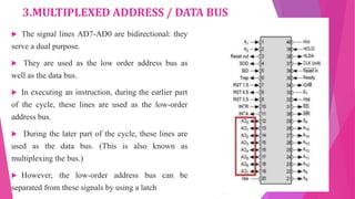
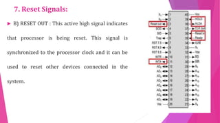
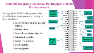
The document describes the pin diagram of the 8085 microprocessor. It discusses the various pin groups and their functions:
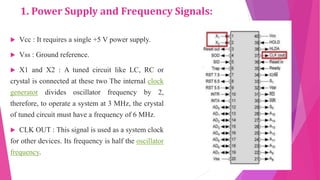
1) Power supply and clock pins provide power and clock signals.
2) Address pins carry the memory address.
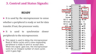
3) Control signals include READ, WRITE and ALE to control data transfer.
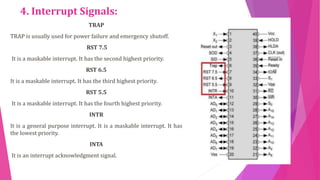
4) Interrupt pins handle different priority interrupts.
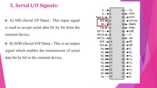
5) Serial I/O pins manage serial communication.
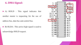
6) DMA signals control direct memory access.
7) Reset pins initialize and synchronize the system on reset.


![2. Address Bus:
Address Bus[A8 – A15]
These pins carry the higher order of address bus.
The address is sent from microprocessor to
memory.
It carries the most significant 8-bit of memory
I/O address.](https://image.slidesharecdn.com/5-200630105818/85/PINDIAGRAM-OF-8085-MICROPROCESSOR-4-320.jpg)