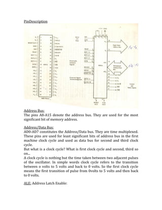
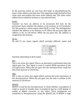
9953330565 Low Rate Call Girls In Rohini Delhi NCR
Pin 8085
1. Introduction
In the previous articles we saw about the architecture of 8085
microprocessor. Now we have a rough idea about how the instructions,
data's are transferred and processed in 8085 microprocessor. In this
article let us discuss in detail about the various signals involved in
transferring data and executing instructions in microprocessor.
Classification of Signals
The various signals in a microprocessor can be classified as
Power supply and Frequency signals: Signals which aids in supplying
power and generating frequency are associated with this type. Pins like
Vcc and ground are classified under this type.
Address signals: Signals associated with the lower order address bus
and time multiplexed higher order address bus comes under this type of
signals.
Data Signals: Signals associated with data bus comes under this type.
Control and Status Signals: Signals which are associated with timing and
control unit such HOLD, RW’, WR’ etc. comes under this type of signals.
Interrupt Signals: We know that signals like TRAP, RST 5.5 etc. are
interrupt signals. Such signals come under this category.
Serial I/O signals: These signals are used for giving serial input and
output data. Signals like SID, SOD come under this category.
Acknowledgement Signals: Signals like INTA’, HLDA acts as
acknowledgement signal for 8085 microprocessor.
2. PinDescription
Address Bus:
The pins A8-A15 denote the address bus. They are used for the most
significant bit of memory address.
Address/Data Bus:
AD0-AD7 constitutes the Address/Data bus. They are time multiplexed.
These pins are used for least significant bits of address bus in the first
machine clock cycle and used as data bus for second and third clock
cycle.
But what is a clock cycle? What is first clock cycle and second, third so
on...
A clock cycle is nothing but the time taken between two adjacent pulses
of the oscillator. In simple words clock cycle refers to the transition
between o volts to 5 volts and back to 0 volts. So the first clock cycle
means the first transition of pulse from 0volts to 5 volts and then back
to 0 volts.
ALE: Address Latch Enable:
3. In the previous article we saw how ALE helps in demultiplexing the
lower order address and data bus. This signal goes high during the first
clock cycle and enables the lower order address bits. The lower order
address bus is added to memory or any external latch.
IO/M’:
Consider we have an address to be processed. But how do the
processors know whether the address is for memory or I/O functions?
For this purpose a status signal called IO/M’ is used. This distinguishes
whether the address is for memory or IO. When this pin goes high, the
address is for an I/O device. While the pin goes low, the address is
assigned for the memory.
S0-S1:
S0 and S1 are status signals which provides different status and
functions depending on their status.
RD’:
This is an active low signal. That is, an operation is performed when the
signal goes low. This signal is used to control READ operation of the
microprocessor. When this pin goes low the microprocessor reads the
data from memory or I/O device.
WR’:
WR’ is also an active low signal which controls the write operations of
the microprocessor. When this pin goes low, the data is written to the
memory or I/O device.
READY:
READY is used by the microprocessor to check whether a peripheral is
ready to accept or transfer data. A peripheral may be a LCD display or
analog to digital converter or any other. These peripherals are
connected to microprocessor using the READY pin. If READY is high
4. then the periphery is ready for data transfer. If not the microprocessor
waits until READY goes high.
HOLD:
This indicates if any other device is requesting the use of address and
data bus. Consider two peripheral devices. One is the LCD and the other
Analog to Digital converter. Suppose if analog to digital converter is
using the address and data bus and if LCD requests the use of address
and data bus by giving HOLD signal, then the microprocessor transfers
the control to the LCD as soon as the current cycle is over. After the LCD
process is over, the control is transferred back to analog and digital
converter.
HLDA:
HLDA is the acknowledgment signal for HOLD. It indicates whether the
HOLD signal is received or not. After the execution of HOLD request,
HLDA goes low.
INTR:
INTR is an interrupt request signal. It has the lowest priority among the
interrupts. INTR can be enabled or disabled by using software.
Whenever INTR goes high the microprocessor completes the current
instruction which is being executed and then acknowledges the INTR
signal and processes it.
INTA’:
Whenever the microprocessor receives interrupt signal. It has to be
acknowledged. This acknowledgement is done by INTA’. So whenever
the interrupt is received INTA’ goes high.
RST 5.5, 6.5, 7.5:
These are nothing but the restart interrupts. They insert an internal
restart function automatically.
All the above mentioned interrupts are maskable interrupts. That is,
they can be enabled or disabled using programs.
TRAP:
Among the interrupts of 8085 microprocessor, TRAP is the only non-
maskable interrupt. It cannot be enabled or disabled using a program. It
has the highest priority among the interrupts.
PRIORITY ORDER (From highest to lowest)
5. TRAP
RST 7.5
RST 6.5
RST 5.5
INTR
RESET IN’:
This pin resets the program counter to 0 and resets interrupt enable
and HLDA flip-flops. The CPU is held in reset condition until this pin is
high. However the flags and registers won’t get affected except for
instruction register.
RESET OUT:
This pin indicates that the CPU has been reset by RESET IN’.
X1 X2:
These are the terminals which are connected to external oscillator to
produce the necessary and suitable clock operation.
CLK:
Sometimes it is necessary for generating clock outputs from
microprocessors so that they can be used for other peripherals or other
digital IC’s. This is provided by CLK pin. Its frequency is always same as
the frequency at which the microprocessor operates.
SID:
This pin provides serial input data. The serial data on this pin is loaded
into the seventh bit of the accumulator when RIM instruction is
executed.
RIM stands for READ INTERRUPT MASK, which checks whether the
interrupt is masked or not.
SOD:
This pin provides the serial output data. The serial data on this pin
delivers its output to the seventh bit of the accumulator when SIM
instruction is executed.
6. Vcc and Vss:
Vcc is +5v pin and Vss is ground pin.
Thus the pin diagram and signals of 8085 microprocessor are explained
in detail.