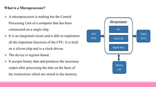
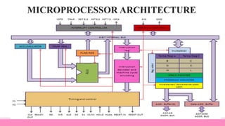
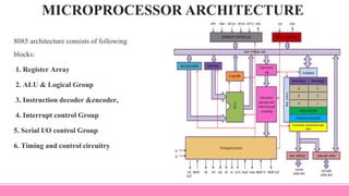
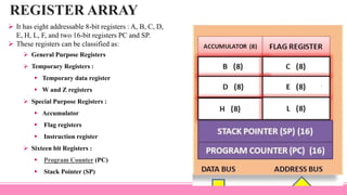
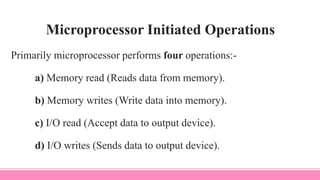
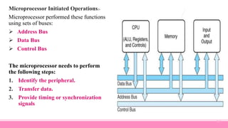
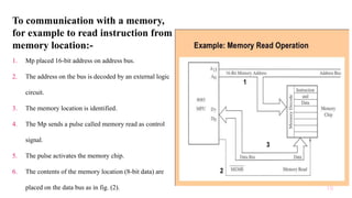
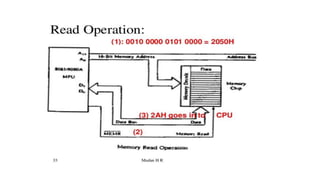
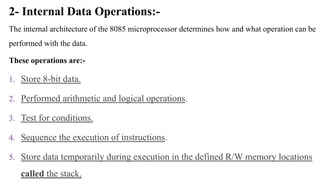
MICROPROCESSOR ARCHITECTURE AND
ITS OPERATIONS
By
Mrs.B.RAMA PRABHA,
ASSISTANT PROFESSOR,
DEPARTMENT OF COMPUTER SCIENCE,
K.C.S.KASI NADAR COLLEGE OF ARTS & SCIENCE
What is a Microprocessor?
 A microprocessor is nothing but the Central
Processing Unit of a computer that has been
constructed on a single chip.
 It is an integrated circuit and is able to implement
all the important functions of the CPU. It is built
on a silicon chip and is a clock-driven.
 The device is register-based.
 It accepts binary data and produces the necessary
output after processing the data on the basis of
the instructions which are stored in the memory.
MICROPROCESSOR ARCHITECTURE
8085 architecture consists of following
blocks:
1. Register Array
2. ALU & Logical Group
3. Instruction decoder &encoder,
4. Interrupt control Group
5. Serial I/O control Group
6. Timing and control circuitry
REGISTER ARRAY
 It has eight addressable 8-bit registers : A, B, C, D,
E, H, L, F, and two 16-bit registers PC and SP.
 These registers can be classified as:
 General Purpose Registers
 Temporary Registers :
 Temporary data register
 W and Z registers
 Special Purpose Registers :
 Accumulator
 Flag registers
 Instruction register
 Sixteen bit Registers :
 Program Counter (PC)
 Stack Pointer (SP)
General purpose register
There are 6 general purpose registers in
8085 processor,
 i.e. B, C, D, E, H & L. Each register
can hold 8-bit data.
 These registers can work in pair to hold
16-bit data and their pairing
combination is like B-C, D-E & H-L.
Register Array
6
Temporary Register:
 It is an 8-bit register associated
with the ALU. It holds data during
an arithmetic/logical operation.
 It is used by the microprocessor.
 It is not accessible to
programmer.
Register Array
7
Special Purpose Register:
Accumulator (A):
 The accumulator is an 8-bit register
associated with the ALU.
 The register 'A' is an accumulator in
the 8085.
 It is used to hold one of the
operands of an arithmetic and
logical operation.
 The final result of an arithmetic
or logical operation is also placed
in the accumulator.
Register Array
8
Special Purpose Register:
Instruction Register:
The instruction register holds the
opcode (operation code or instruction
code) of the instruction which is being
decoded and executed.
9
Special Purpose Register:
 Flags Register:
 The Intel 8085 microprocessor contains
five flip-flops to serve as a status flags.
The flip-flops are reset or set according to
the conditions which arise during an
arithmetic or logical operation.
 The five status flags of Intel 8085 are:
 Carry Flag (CS)
 Parity Flag (P)
 Auxiliary Carry Flag (AC)
 Zero Flag(Z)
 Sign Flag(S)
10
16 bit Register:
Program Counter (PC):
 It is a 16-bit special purpose register.
 It is used to hold the address of memory of
the next instruction to be executed.
 It keeps the track of the instruction in a
program while they are being executed.
 The microprocessor increments the content
of the next program counter during the
execution of an instruction
11
16 bit Register:
Stack Pointer (SP):
 It is a 16-bit special function register used as
memory pointer.
 A stack is nothing but a portion of RAM.
 In the stack, the contents of only those registers
are saved, which are needed in the later part of the
program.
12
The Arithmetic and Logic Unit:
 ALU performs the arithmetic and logical operations.
The result of an operation is stored in Accumalator
Instruction decoder and machine cycle encoder:
 Decodes the op-code stored in the Instruction Register (IR) and establishes the sequence of events to
follow.
 Encodes it and transfer to the timing & control unit to perform the execution of the instruction.
Timing and control circuitry
 works as the brain of the CPU
 For proper sequence and synchronization of all the operations of MP, this unit generates all the
timing and control signals necessary for communication between microprocessor and peripherals.
13
Interrupt Control group
 Interrupt:- Occurrence of an external disturbance
 After servicing the interrupt, 8085 resumes its normal working sequence
Transfer the control to special routines
Five interrupts: - TRAP, RST7.5, RST6.5, RST5.5, INTR
In response to INTR, it generates INTA signal
Serial I/O control Group
Data transferred on D0- D7 lines is parallel data
But under some condition it is used serial data transfer
Serial data is entered through SID(serial input data) input (received)
Serial data is outputted on SOD(serial output data) input (send)
14
MICRO PROCESSOR OPERATIONS
 The internal Logic design of the microprocessor called its architecture, determine how
and what various operations are performed by the microprocessor.
 The microprocessor is programmable logic device deigned with register ,flip-flop and
timing elements.
 All functions in microprocessor can be classified in three categories:
1. Microprocessor Initiated operations
2. Internal data operations
3. Peripheral (or externally initiated) operations
15
Microprocessor Initiated Operations
Primarily microprocessor performs four operations:-
a) Memory read (Reads data from memory).
b) Memory writes (Write data into memory).
c) I/O read (Accept data to output device).
d) I/O writes (Sends data to output device).
Microprocessor Initiated Operations:-
Microprocessor performed these functions
using sets of buses:
 Address Bus
 Data Bus
 Control Bus
The microprocessor needs to perform
the following steps:
1. Identify the peripheral.
2. Transfer data.
3. Provide timing or synchronization
signals
17
Bus Structure in 8085
Address bus:
 Microprocessor has 16 bit address bus.
 The bus over which the CPU sends out the
address of the memory location is known
as Address bus.
 The address bus is unidirectional.
Data bus:
 8085 Microprocessor has 8 bit data bus. So
it can be used to carry the 8 bit data .
 It is bidirectional.
Control bus :
 The control bus is used for sending control
signals to the memory and I/O devices. 18
19
To communication with a memory,
for example to read instruction from
memory location:-
1. Mp placed 16-bit address on address bus.
2. The address on the bus is decoded by an external logic
circuit.
3. The memory location is identified.
4. The Mp sends a pulse called memory read as control
signal.
5. The pulse activates the memory chip.
6. The contents of the memory location (8-bit data) are
placed on the data bus as in fig. (2).
2- Internal Data Operations:-
The internal architecture of the 8085 microprocessor determines how and what operation can be
performed with the data.
These operations are:-
1. Store 8-bit data.
2. Performed arithmetic and logical operations.
3. Test for conditions.
4. Sequence the execution of instructions.
5. Store data temporarily during execution in the defined R/W memory locations
called the stack.
Internal Data Operations:-
To perform these operations the Microprocessor requires:-
a) Registers.
b) An arithmetic logic unit (ALU) & control logic.
c) Internal buses (paths for information flow).
22
Peripheral or Externally Initiated Operations:-
External devices (or signals) can initiate the following operation for which individual pins on Microprocessor chip are
assigned: Reset, Interrupt, Ready, Hold.
A) Reset: when reset is activated all internal operations are suspended and the program counter is cleared.
B) Interrupt: the Microprocessor can be interrupted from normal execution and asked to execute other instructions called
"service routine" (emergency), Microprocessor resumes its operation after that.
C) Ready: 8085 has pin called ready, if the signal is low Microprocessor enters into wait state, this signal used to
synchronized slower peripherals with Microprocessor.
D) Hold: when hold pin activated by external signal Microprocessor relinquishes control buses and allows the external
peripheral to use the. For example: Hold signal is used in direct memory access data transfer.
23
THANK YOU!!!

8085 MICROPROCESSOR ARCHITECTURE AND ITS OPERATIONS

  • 1.
    MICROPROCESSOR ARCHITECTURE AND ITSOPERATIONS By Mrs.B.RAMA PRABHA, ASSISTANT PROFESSOR, DEPARTMENT OF COMPUTER SCIENCE, K.C.S.KASI NADAR COLLEGE OF ARTS & SCIENCE
  • 2.
    What is aMicroprocessor?  A microprocessor is nothing but the Central Processing Unit of a computer that has been constructed on a single chip.  It is an integrated circuit and is able to implement all the important functions of the CPU. It is built on a silicon chip and is a clock-driven.  The device is register-based.  It accepts binary data and produces the necessary output after processing the data on the basis of the instructions which are stored in the memory.
  • 3.
  • 4.
    MICROPROCESSOR ARCHITECTURE 8085 architectureconsists of following blocks: 1. Register Array 2. ALU & Logical Group 3. Instruction decoder &encoder, 4. Interrupt control Group 5. Serial I/O control Group 6. Timing and control circuitry
  • 5.
    REGISTER ARRAY  Ithas eight addressable 8-bit registers : A, B, C, D, E, H, L, F, and two 16-bit registers PC and SP.  These registers can be classified as:  General Purpose Registers  Temporary Registers :  Temporary data register  W and Z registers  Special Purpose Registers :  Accumulator  Flag registers  Instruction register  Sixteen bit Registers :  Program Counter (PC)  Stack Pointer (SP)
  • 6.
    General purpose register Thereare 6 general purpose registers in 8085 processor,  i.e. B, C, D, E, H & L. Each register can hold 8-bit data.  These registers can work in pair to hold 16-bit data and their pairing combination is like B-C, D-E & H-L. Register Array 6
  • 7.
    Temporary Register:  Itis an 8-bit register associated with the ALU. It holds data during an arithmetic/logical operation.  It is used by the microprocessor.  It is not accessible to programmer. Register Array 7
  • 8.
    Special Purpose Register: Accumulator(A):  The accumulator is an 8-bit register associated with the ALU.  The register 'A' is an accumulator in the 8085.  It is used to hold one of the operands of an arithmetic and logical operation.  The final result of an arithmetic or logical operation is also placed in the accumulator. Register Array 8
  • 9.
    Special Purpose Register: InstructionRegister: The instruction register holds the opcode (operation code or instruction code) of the instruction which is being decoded and executed. 9
  • 10.
    Special Purpose Register: Flags Register:  The Intel 8085 microprocessor contains five flip-flops to serve as a status flags. The flip-flops are reset or set according to the conditions which arise during an arithmetic or logical operation.  The five status flags of Intel 8085 are:  Carry Flag (CS)  Parity Flag (P)  Auxiliary Carry Flag (AC)  Zero Flag(Z)  Sign Flag(S) 10
  • 11.
    16 bit Register: ProgramCounter (PC):  It is a 16-bit special purpose register.  It is used to hold the address of memory of the next instruction to be executed.  It keeps the track of the instruction in a program while they are being executed.  The microprocessor increments the content of the next program counter during the execution of an instruction 11
  • 12.
    16 bit Register: StackPointer (SP):  It is a 16-bit special function register used as memory pointer.  A stack is nothing but a portion of RAM.  In the stack, the contents of only those registers are saved, which are needed in the later part of the program. 12
  • 13.
    The Arithmetic andLogic Unit:  ALU performs the arithmetic and logical operations. The result of an operation is stored in Accumalator Instruction decoder and machine cycle encoder:  Decodes the op-code stored in the Instruction Register (IR) and establishes the sequence of events to follow.  Encodes it and transfer to the timing & control unit to perform the execution of the instruction. Timing and control circuitry  works as the brain of the CPU  For proper sequence and synchronization of all the operations of MP, this unit generates all the timing and control signals necessary for communication between microprocessor and peripherals. 13
  • 14.
    Interrupt Control group Interrupt:- Occurrence of an external disturbance  After servicing the interrupt, 8085 resumes its normal working sequence Transfer the control to special routines Five interrupts: - TRAP, RST7.5, RST6.5, RST5.5, INTR In response to INTR, it generates INTA signal Serial I/O control Group Data transferred on D0- D7 lines is parallel data But under some condition it is used serial data transfer Serial data is entered through SID(serial input data) input (received) Serial data is outputted on SOD(serial output data) input (send) 14
  • 15.
    MICRO PROCESSOR OPERATIONS The internal Logic design of the microprocessor called its architecture, determine how and what various operations are performed by the microprocessor.  The microprocessor is programmable logic device deigned with register ,flip-flop and timing elements.  All functions in microprocessor can be classified in three categories: 1. Microprocessor Initiated operations 2. Internal data operations 3. Peripheral (or externally initiated) operations 15
  • 16.
    Microprocessor Initiated Operations Primarilymicroprocessor performs four operations:- a) Memory read (Reads data from memory). b) Memory writes (Write data into memory). c) I/O read (Accept data to output device). d) I/O writes (Sends data to output device).
  • 17.
    Microprocessor Initiated Operations:- Microprocessorperformed these functions using sets of buses:  Address Bus  Data Bus  Control Bus The microprocessor needs to perform the following steps: 1. Identify the peripheral. 2. Transfer data. 3. Provide timing or synchronization signals 17
  • 18.
    Bus Structure in8085 Address bus:  Microprocessor has 16 bit address bus.  The bus over which the CPU sends out the address of the memory location is known as Address bus.  The address bus is unidirectional. Data bus:  8085 Microprocessor has 8 bit data bus. So it can be used to carry the 8 bit data .  It is bidirectional. Control bus :  The control bus is used for sending control signals to the memory and I/O devices. 18
  • 19.
    19 To communication witha memory, for example to read instruction from memory location:- 1. Mp placed 16-bit address on address bus. 2. The address on the bus is decoded by an external logic circuit. 3. The memory location is identified. 4. The Mp sends a pulse called memory read as control signal. 5. The pulse activates the memory chip. 6. The contents of the memory location (8-bit data) are placed on the data bus as in fig. (2).
  • 21.
    2- Internal DataOperations:- The internal architecture of the 8085 microprocessor determines how and what operation can be performed with the data. These operations are:- 1. Store 8-bit data. 2. Performed arithmetic and logical operations. 3. Test for conditions. 4. Sequence the execution of instructions. 5. Store data temporarily during execution in the defined R/W memory locations called the stack.
  • 22.
    Internal Data Operations:- Toperform these operations the Microprocessor requires:- a) Registers. b) An arithmetic logic unit (ALU) & control logic. c) Internal buses (paths for information flow). 22
  • 23.
    Peripheral or ExternallyInitiated Operations:- External devices (or signals) can initiate the following operation for which individual pins on Microprocessor chip are assigned: Reset, Interrupt, Ready, Hold. A) Reset: when reset is activated all internal operations are suspended and the program counter is cleared. B) Interrupt: the Microprocessor can be interrupted from normal execution and asked to execute other instructions called "service routine" (emergency), Microprocessor resumes its operation after that. C) Ready: 8085 has pin called ready, if the signal is low Microprocessor enters into wait state, this signal used to synchronized slower peripherals with Microprocessor. D) Hold: when hold pin activated by external signal Microprocessor relinquishes control buses and allows the external peripheral to use the. For example: Hold signal is used in direct memory access data transfer. 23
  • 24.