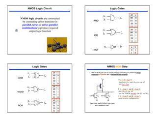
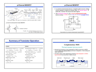
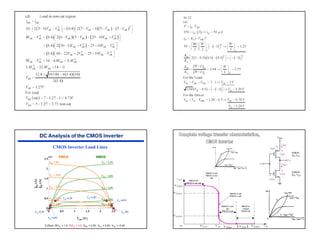
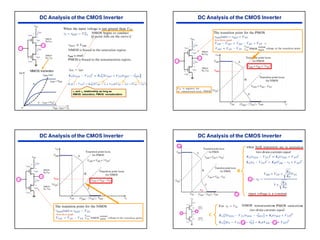
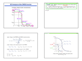
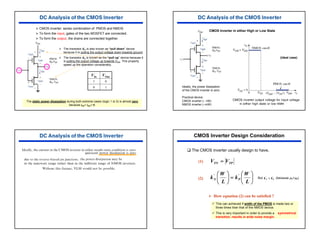
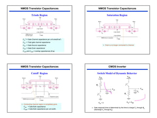
1. The document discusses NMOS and CMOS inverter circuits. It describes the operation of an NMOS inverter using an enhancement load, depletion load, and resistor load.
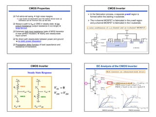
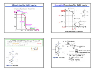
2. A CMOS inverter uses both an NMOS and PMOS transistor to provide complementary output signals. It has advantages over NMOS inverters like zero static power dissipation and full voltage swing at the output.
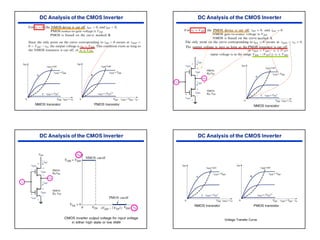
3. The voltage transfer curve of a CMOS inverter is discussed along with the load lines showing the different operating regions of the NMOS and PMOS transistors.
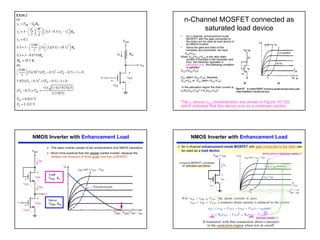
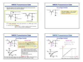
![10
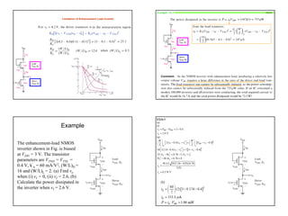
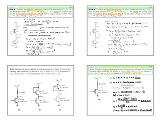
NMOS Inverter with Depletion Load (cont.)
Case I: when VI<VTND (drive is
cutoff): No drain current conduct
in either transistor. That means
the load transistor must be in the
linear region of the operation and
the output current can be
expressed as fellows
iDL(linear)=KL[2(VGSL - VTNL)VDSL -
VDSL
2]
Since VGSL=0, and iDL=0
0=-KL[2VTNLVDSL + VDSL
2]
Which gives VDSL=0 thus
VO= VDD
This is the advantage of the
depletion load inverter over the
enhancement load inverter.
When vI > VTND
Just greater than
NMOS Inverter with Depletion Load
NMOS Inverter with Depletion Load
This implies that input voltage is constant
as the Q-point passes this region.
NMOS Inverter with Depletion Load
This implies that input and output voltages
are not linear in this region.](https://image.slidesharecdn.com/chap16-1-nmos-inverter-220920140724-0485b5b8/85/Chap16-1-NMOS-Inverter-pdf-10-320.jpg)
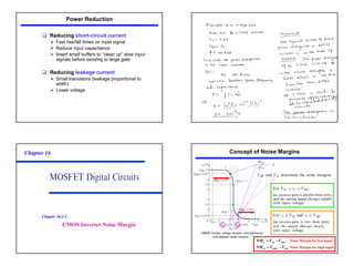
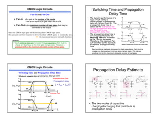
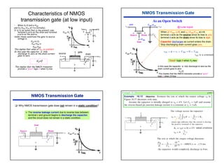
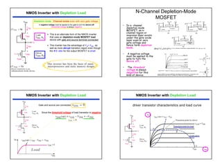
![40
Switch-level model
Delay estimation using switch-
level model (for general RC
circuit):
Rn CL
[ ]
=
−
=
=
=
−
=
→
=
=
→
=
∫
0
1
0
1
0
1
ln
)
ln(
)
ln(
1
0
V
V
RC
V
V
RC
t
dV
V
RC
t
t
t
dV
V
RC
dt
R
V
I
dV
I
C
dt
dt
dV
C
I
p
V
V
p
Switch-level model
• For fall delay tphl, V0=Vcc, V1=Vcc/2
L
p
plh
L
n
phl
p
CC
CC
p
C
R
t
C
R
t
RC
t
V
V
RC
V
V
RC
t
69
.
0
69
.
0
)
5
.
0
ln(
ln
ln 2
1
0
1
=
=
=
=
=
Standard RC-delay
equations
Chapter 16
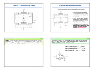
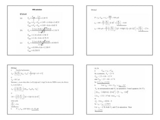
Transmission Gates
Chapter 16.6
Transmission Gates
¾ Use of transistors as switches between driving circuits and load
circuits are called transmission gates because switches can transmit
information from one circuit to another.
¾ NMOS and CMOS transmission gate.](https://image.slidesharecdn.com/chap16-1-nmos-inverter-220920140724-0485b5b8/85/Chap16-1-NMOS-Inverter-pdf-40-320.jpg)