Download to read offline


![References
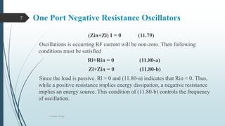
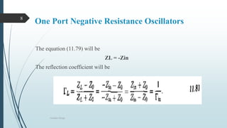
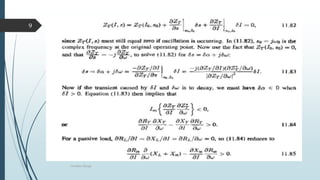
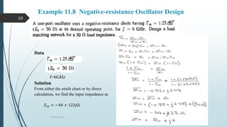
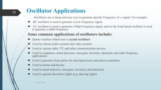
Oscillator Design
31
[1] Microwave Engineering 2nd edition David M. Pozar University of Massachusetts at Amherst
[2] J. B. Beyer. S. N Parasad. R. C. Becker. J.E Nordman. And G. K. Hohenwarter, “MESFET Distributed Amplifier
Design Guidelines,” IEEE Trans. Microwave Theory and techniques. Vol.MTT-32, pp.268-275, March 1984.
eyesha.sajid@gmail.com
farnaz.nawaz@gmail.com
rimsha.ashraf319@gmail.com
sobia.arshad26@gmail.com
Contacts
The End](https://image.slidesharecdn.com/oscillatordesignm-200627160641/85/Oscillator-Design-M-Pozar-2nd-edition-31-320.jpg)

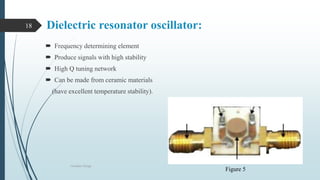
The document provides an overview of oscillator design. It discusses the principles of one-port negative resistance oscillators and transistor oscillators. It describes how dielectric resonator oscillators use a high-Q resonator to produce stable signals. Examples are provided on designing negative resistance and dielectric resonator oscillators. Common applications of oscillators include generating clock signals for devices. Advantages are portability and adjustable frequencies, while disadvantages include bulkiness and poor frequency stability.


![RF Module Design - [Chapter 7] Voltage-Controlled Oscillator](https://cdn.slidesharecdn.com/ss_thumbnails/rfch7-150613070347-lva1-app6892-thumbnail.jpg?width=640&height=640&fit=bounds)


