(1) This document describes the design of a multi-channel UART controller based on FPGA that can connect to multiple peripherals simultaneously. Traditional UART controllers are limited to connecting only one peripheral.
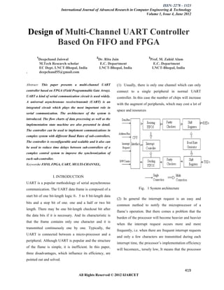
(2) The proposed design uses FIFO buffers and parallel processing to allow data from multiple channels to be transmitted and received simultaneously, reducing processing delays. Interrupt requests are managed to reduce the processing burden on the microprocessor.
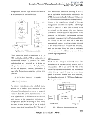
(3) The design aims to make better use of the microprocessor's wide data bus by transmitting multiple bytes of data at once, rather than just one byte as in traditional designs. This is implemented using Verilog HDL on an FPGA for reconfigurability and scal


![ISSN: 2278 – 1323
International Journal of Advanced Research in Computer Engineering & Technology
Volume 1, Issue 4, June 2012
8. Delvai M,Eisenmann U, Elmenrichs W Intelligent UART module
for real-time applications. First Workshop on Intelligent Solutions in
Embedded Systems,2002;1 77—185.
9. X., Yang, “Industrial Data Communication and Control Networks”,
V. CONCLUTION
Beijing: TUP, 2003.6[9] B. Zeidman, “Designing with FPGAs &
The paper presents design method of asynchronous FIFO CPLDs”, CMP Books, 2002
and structure of the controller. This controller is 10. C. E. Cummings, “Simulation and Synthesis Techniques for
Asynchronous FIFO Design with Asynchronous Pointer
designed with FIFO circuit block and UART (Universal Comparisons”, SNUG San Jose 2002
Asynchronous Receiver Transmitter) circuit block within
FPGA to implement communication in modern complex
control systems quickly and effectively. Form the
communication sequence diagrams; it is easily to know
that this controller can be used to implement
communication when master equipment and slaver
equipment are set at different Baud Rate. It also can be
used to reduce synchronization error between sub-
systems in a system with several sub-systems. The
controller is reconfigurable and scalable.
REFERENCES
1. S. E. Lyshevski, “Control Systems Theory with Engineering
Applications”, Birkhauser Boston, 2001.
2. Free scale semiconductor, Inc MPC860 Power QUICCTM family
user’s manua1.2004.
3. Li SG Gao D Y Nie PQ Study on multi task management unit MTU
of embedded micro NCS, Acta Aeronautical et Astronautic Sinica
2000;21(2):134-137 in Chinese.
4. Liu L, Gao D, Y Zhang SB, et a1.Design of EM FPU in
embedded microprocessor Act a Aeronatuticaet Astronautics
Sinica2001;22(4):308-31 1.[in Chinese]
5. Yean del J, Thulborn D, Jones S. An online testable UART
implemented using IFIS.1 5th IEEE VLSI Test et Astronautic
Symposium ,1997;344-349.
6. Elmenreich W, Delvai M, Time triggered communication with
UARTs.4th IEEE International Workshop on Factory
Communication Systems,2002;97-104.
7. Gallo R, Delvai M,Elmenreich W,eta1.Revision an d veil
fiction of an enhanced UART.IEEE International Workshop on
Factory Communication Systems,2004;315-318.
426
All Rights Reserved © 2012 IJARCET](https://image.slidesharecdn.com/419-426-120630094726-phpapp02/85/419-426-8-320.jpg)