


![To subscribe to the PARC Innovations Update e-newsletter or blog, or to follow us on Twitter, go to http://www.parc.com/about/subscribe.html For more information, please contact: Ana Arias ana.arias@ parc.com Jennifer Ernst, Business Development [email_address]](https://image.slidesharecdn.com/printedflexelectronicsttiv02252010parc-100302010536-phpapp01/85/Flexible-Electronics-15-320.jpg)

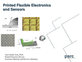
The document discusses advancements in printed flexible electronics, highlighting their potential applications and challenges in commercialization. It covers various technologies, such as organic and inorganic materials, and the development of printed sensors and displays, emphasizing the need for innovative manufacturing techniques and partnerships. The document also mentions specific products and projects, illustrating the current landscape of flexible electronics and their future possibilities.