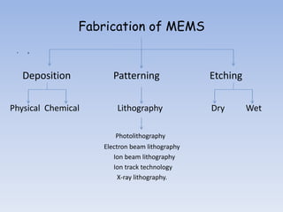
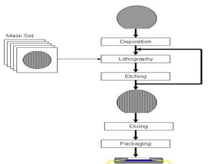
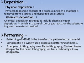
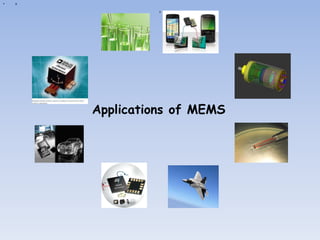
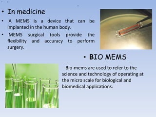
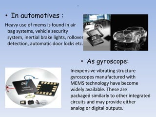
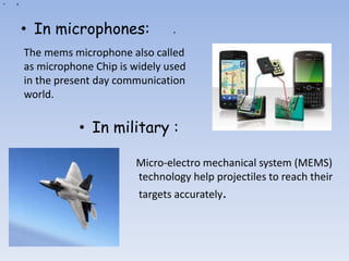
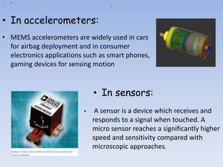
SHREEJEE INSTITUTE OF
TECHNOLOGY AND MANAGEMENT
Micro electro mechnical system
• Guided By:- Mr. Prakash
Singh Panwar
• By:- Krishna Rathor
• EC BRANCH 1ST YEAR
MEMS is a technology of very small devices. It is a combination of
mechanical functions and electrical functions on the same chip
using micro fabrication technology.
MEMS are made up of components between 1 to 100
micrometers in size
MEMS devices generally range in size from 20 micrometers to a
millimeter
• Actuator
• Ambient intelligence
• Energy scavengers
• Getters
• Sensor (M,T,C,R,E)
a
• a
Fabrication of MEMS
Deposition Patterning Etching
Physical Chemical Lithography Dry Wet
Photolithography
Electron beam lithography
Ion beam lithography
Ion track technology
X-ray lithography.
a
• a
a
Deposition –
Physical deposition :
Physical deposition consists of a process in which a material is
removed from a target, and deposited on a surface
Chemical deposition :
Chemical deposition techniques include chemical vapor
deposition, in which a stream of source gas reacts on the substrate
to grow the material desired.
Patterning –
• Patterning of MEMS is the transfer of a pattern into a material.
• Lithography is a widely used process in patterning of mems .
• Examples of lithography are– Photolithography, Electron beam
lithography, Ion beam lithography, Ion track technology, X-ray
lithography.
Etching
• a
• Wet Etching :
• Wet chemical etching
consists in selective
removal of material by
dipping a substrate
into a solution that
dissolves it.
• The chemical nature
of this etching process
provides a good
selectivity
• Dry Etching :
• Dry etching can be done in
three ways and they are –
a) Reactive ion etching (RIE)
b) Sputter etching
c) Vapor phase etching.
Designing an MST/MEMS device is basically an
iterative process; the design is put into a
simulation loop, improved and resubmitted for
simulation until the design fits the demands.
It is seldom possible to use design methodologies
and tools from traditional industries working with
larger dimensions due to the fundamental
differences related to the order of magnitude of
the typical dimensions
a
Metal can package
Plastic package
Ceramic package
a
• a
a
• a
Applications of MEMS
a
• a
• A MEMS is a device that can be
implanted in the human body.
• MEMS surgical tools provide the
flexibility and accuracy to perform
surgery.
• In medicine
• BIO MEMS
• Bio-mems are used to refer to the
science and technology of operating at
the micro scale for biological and
biomedical applications.
a
• In automotives :
• As gyroscope:
Heavy use of mems is found in air
bag systems, vehicle security
system, inertial brake lights, rollover
detection, automatic door locks etc.
Inexpensive vibrating structure
gyroscopes manufactured with
MEMS technology have become
widely available. These are
packaged similarly to other integrated
circuits and may provide either
analog or digital outputs.
a
• a
• In microphones:
Micro-electro mechanical system (MEMS)
technology help projectiles to reach their
targets accurately.
• In military :
The mems microphone also called
as microphone Chip is widely used
in the present day communication
world.
a
• a
• In accelerometers:
• MEMS accelerometers are widely used in cars
for airbag deployment and in consumer
electronics applications such as smart phones,
gaming devices for sensing motion
• In sensors:
• A sensor is a device which receives and
responds to a signal when touched. A
micro sensor reaches a significantly higher
speed and sensitivity compared with
microscopic approaches.
a
• Apart from these applications mems are also used in many fields in
the present world
• They are used to detect earth quakes, in gas shut off, in shock and
tilt sensing
• Inkjet printers and micro scanners also involve the use of mems.
• Mems is used in Optical switching technology in which, switching
technology and alignment for data communications is done.
a
• a
Advantages and disadvantages
 Minimize energy
and materials.
Improved
reproducibility.
 Improved accuracy
and reliability.
 Increased selectivity
and sensitivity.
 Farm establishment
requires huge
investments.
 Micro-components
are costly compared
to macro components.
 Design includes very
much complex
procedures
Conclusion
• This enabling technology
promises to create
entirely new categories of
products.
• MEMS will be the
indispensible factor in
advancing technology
• As with all emerging
technologies had been
predicted to revolutionize
technology and our lives

micro electro mechnical system

  • 1.
    SHREEJEE INSTITUTE OF TECHNOLOGYAND MANAGEMENT Micro electro mechnical system • Guided By:- Mr. Prakash Singh Panwar • By:- Krishna Rathor • EC BRANCH 1ST YEAR
  • 2.
    MEMS is atechnology of very small devices. It is a combination of mechanical functions and electrical functions on the same chip using micro fabrication technology. MEMS are made up of components between 1 to 100 micrometers in size MEMS devices generally range in size from 20 micrometers to a millimeter
  • 3.
    • Actuator • Ambientintelligence • Energy scavengers • Getters • Sensor (M,T,C,R,E)
  • 4.
    a • a Fabrication ofMEMS Deposition Patterning Etching Physical Chemical Lithography Dry Wet Photolithography Electron beam lithography Ion beam lithography Ion track technology X-ray lithography.
  • 5.
  • 6.
    a Deposition – Physical deposition: Physical deposition consists of a process in which a material is removed from a target, and deposited on a surface Chemical deposition : Chemical deposition techniques include chemical vapor deposition, in which a stream of source gas reacts on the substrate to grow the material desired. Patterning – • Patterning of MEMS is the transfer of a pattern into a material. • Lithography is a widely used process in patterning of mems . • Examples of lithography are– Photolithography, Electron beam lithography, Ion beam lithography, Ion track technology, X-ray lithography.
  • 7.
    Etching • a • WetEtching : • Wet chemical etching consists in selective removal of material by dipping a substrate into a solution that dissolves it. • The chemical nature of this etching process provides a good selectivity • Dry Etching : • Dry etching can be done in three ways and they are – a) Reactive ion etching (RIE) b) Sputter etching c) Vapor phase etching.
  • 9.
    Designing an MST/MEMSdevice is basically an iterative process; the design is put into a simulation loop, improved and resubmitted for simulation until the design fits the demands. It is seldom possible to use design methodologies and tools from traditional industries working with larger dimensions due to the fundamental differences related to the order of magnitude of the typical dimensions
  • 10.
  • 11.
    Metal can package Plasticpackage Ceramic package
  • 12.
  • 13.
  • 15.
    a • a • AMEMS is a device that can be implanted in the human body. • MEMS surgical tools provide the flexibility and accuracy to perform surgery. • In medicine • BIO MEMS • Bio-mems are used to refer to the science and technology of operating at the micro scale for biological and biomedical applications.
  • 16.
    a • In automotives: • As gyroscope: Heavy use of mems is found in air bag systems, vehicle security system, inertial brake lights, rollover detection, automatic door locks etc. Inexpensive vibrating structure gyroscopes manufactured with MEMS technology have become widely available. These are packaged similarly to other integrated circuits and may provide either analog or digital outputs.
  • 17.
    a • a • Inmicrophones: Micro-electro mechanical system (MEMS) technology help projectiles to reach their targets accurately. • In military : The mems microphone also called as microphone Chip is widely used in the present day communication world.
  • 18.
    a • a • Inaccelerometers: • MEMS accelerometers are widely used in cars for airbag deployment and in consumer electronics applications such as smart phones, gaming devices for sensing motion • In sensors: • A sensor is a device which receives and responds to a signal when touched. A micro sensor reaches a significantly higher speed and sensitivity compared with microscopic approaches.
  • 19.
    a • Apart fromthese applications mems are also used in many fields in the present world • They are used to detect earth quakes, in gas shut off, in shock and tilt sensing • Inkjet printers and micro scanners also involve the use of mems. • Mems is used in Optical switching technology in which, switching technology and alignment for data communications is done.
  • 20.
    a • a Advantages anddisadvantages  Minimize energy and materials. Improved reproducibility.  Improved accuracy and reliability.  Increased selectivity and sensitivity.  Farm establishment requires huge investments.  Micro-components are costly compared to macro components.  Design includes very much complex procedures
  • 21.
    Conclusion • This enablingtechnology promises to create entirely new categories of products. • MEMS will be the indispensible factor in advancing technology • As with all emerging technologies had been predicted to revolutionize technology and our lives