Download as PDF, PPTX
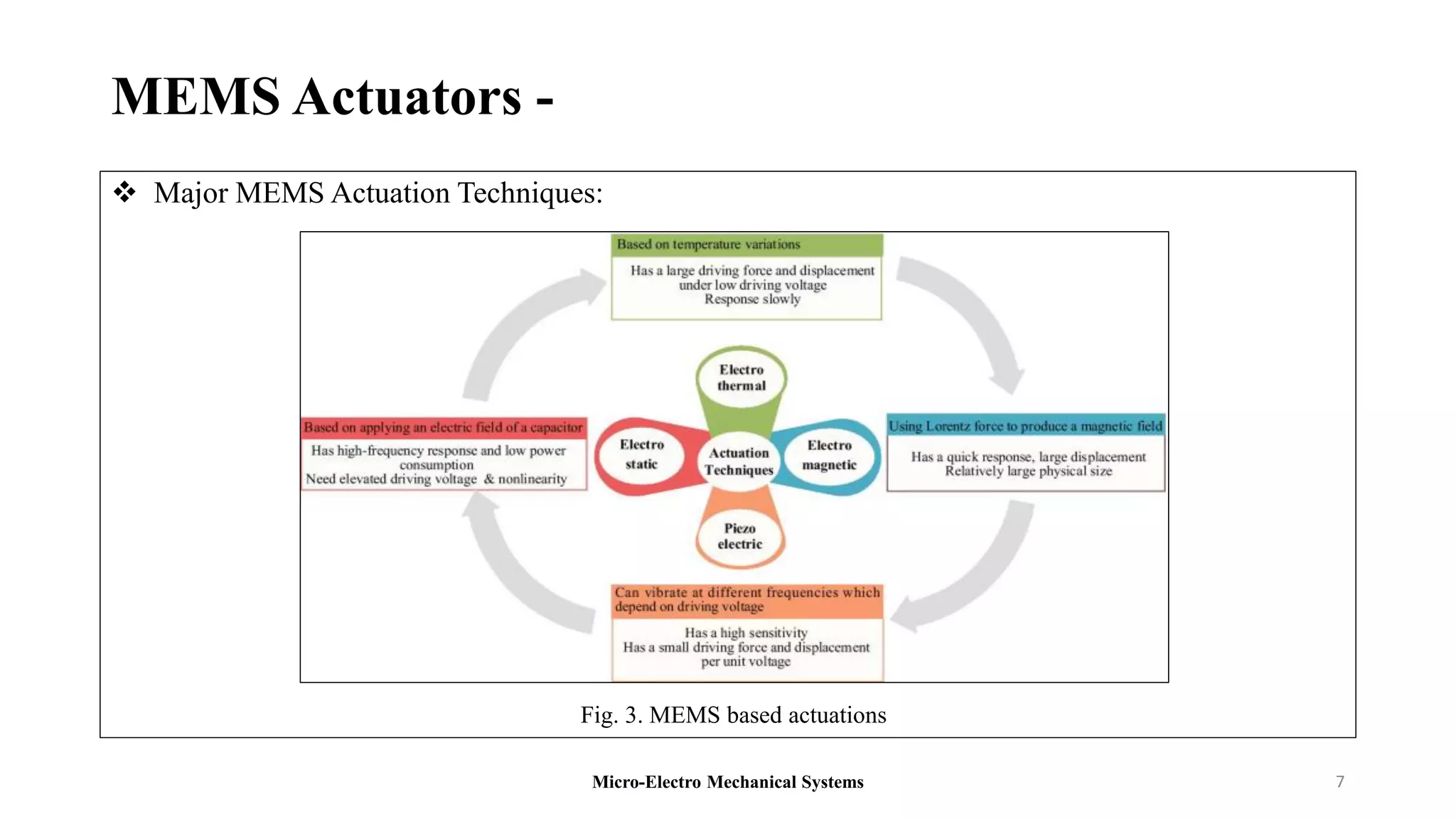
![MEMS Transducers -
The current MEMS-based technology is operational with the following transduction.
1. Tribo-electric – Glass (𝑆𝑖𝑂4), Silk, Hard rubber ( 𝐶5𝐻8 𝑛), fur.
2. Electrostatic – Amber Rod (𝐶10𝐻16𝑂).
3. Piezoelectric – Quartz (𝑆𝑖𝑂2), Lead Zirconate Titanate (𝑃𝑍𝑇), Polyvinylidene Fluoride
(𝑃𝑉𝐷𝐹), Zinc Oxide (𝑍𝑛𝑂), Bone, DNA.
4. Ferroelectric – Barium Titanate (𝐵𝑎𝑇𝑖𝑂3), Lead Titanate (𝑃𝑏𝑇𝑖𝑂3) Lead Zirconate Titanate
(PZT) and Rochelle salt (i.e. Potassium Sodium Tartrate Tetra-hydrate
(𝐾𝑁𝑎𝐶4𝐻4𝑂6. 4𝐻2𝑂))
5. Magnetostrictive – Cobalt Ferrite ( C𝑜𝐹𝑒2𝑂4 𝐶𝑜𝑂. 𝐹𝑒2𝑂3 ), Alloys like Terfenol-D
[Terbium-Iron-Dysprosium (𝑇𝑏𝑥𝐷𝑦1−𝑥𝐹𝑒2 )], Galfenol (Gallium-Iron), Metglas 2605SC
[Metallic Glass]
6. Magnetic – Iron, Steel, Nickel, Cobalt.
Micro-Electro Mechanical Systems 5](https://image.slidesharecdn.com/2mems-sensorstransducersactuators-230907081724-c1f9eede/75/2_MEMS-Sensors-Transducers-Actuators-pdf-5-2048.jpg)

The document provides an overview of MEMS (Micro-Electro-Mechanical Systems) sensors, transducers, actuators, and their fabrication materials and processes. It describes various sensor domains, different types of transducers and actuators, and the materials used in manufacturing MEMS devices. Additionally, it explains the properties of fabrication materials and the concept of die per wafer in the context of MEMS technology.