Download to read offline


MEMS, or Micro-Electro Mechanical Systems, involve the design and development of miniature integrated devices combining mechanical and electrical components, utilizing interdisciplinary engineering. These systems offer advantages such as small size, low power consumption, and ease of integration, but also face challenges like reliability and power transfer issues. Applications range from navigation and environmental studies to biomedical solutions and military operations.
Introduction to MEMS and contents overview including definitions, characteristics, and applications.
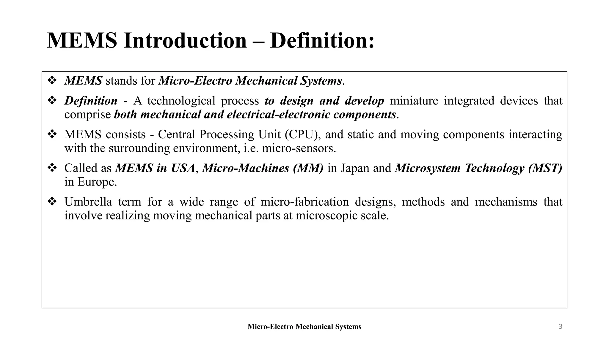
MEMS defined as Micro-Electro Mechanical Systems including components like CPU and micro-sensors.
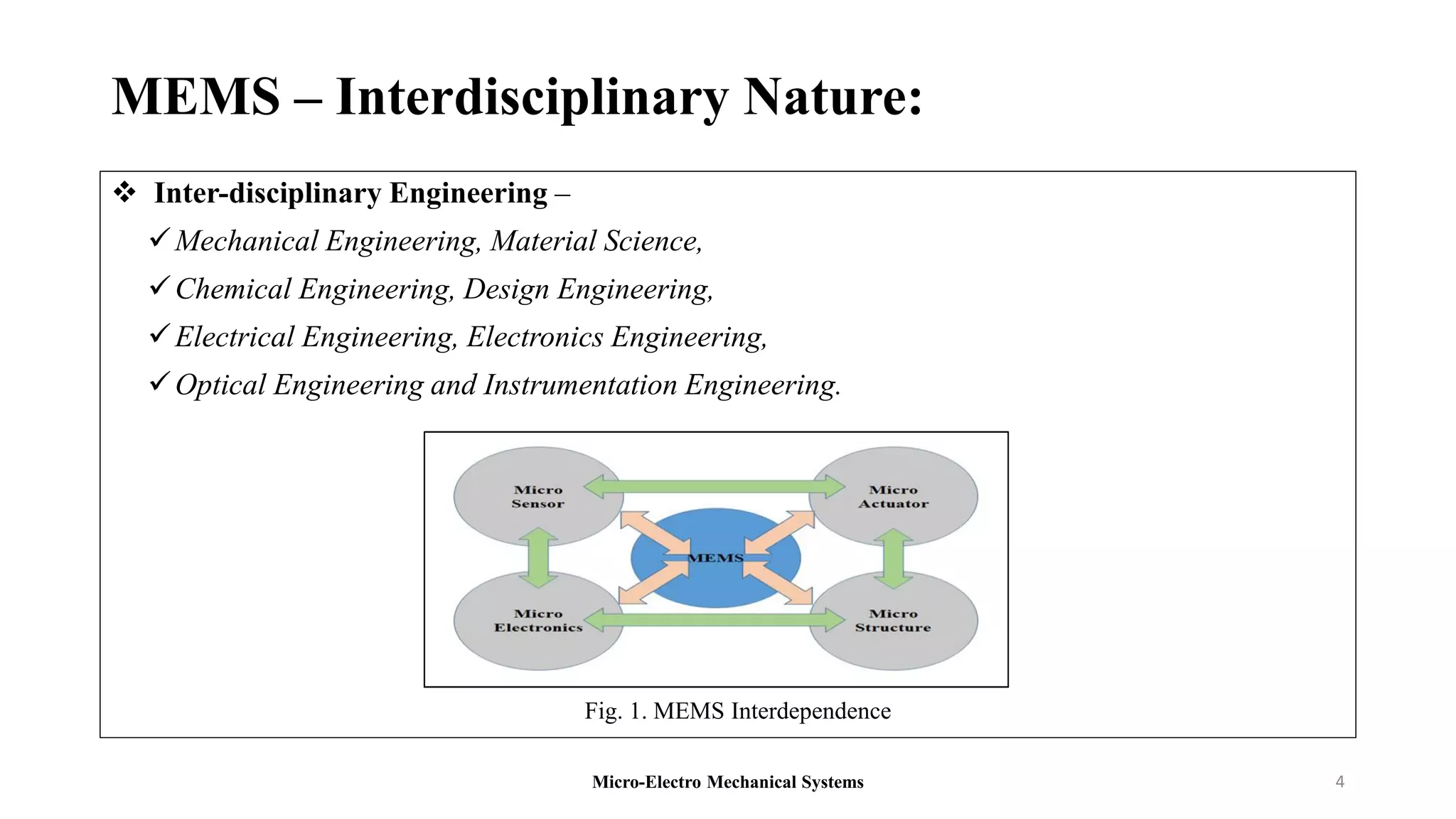
MEMS integrates various engineering disciplines including mechanical, electrical, and optical engineering.
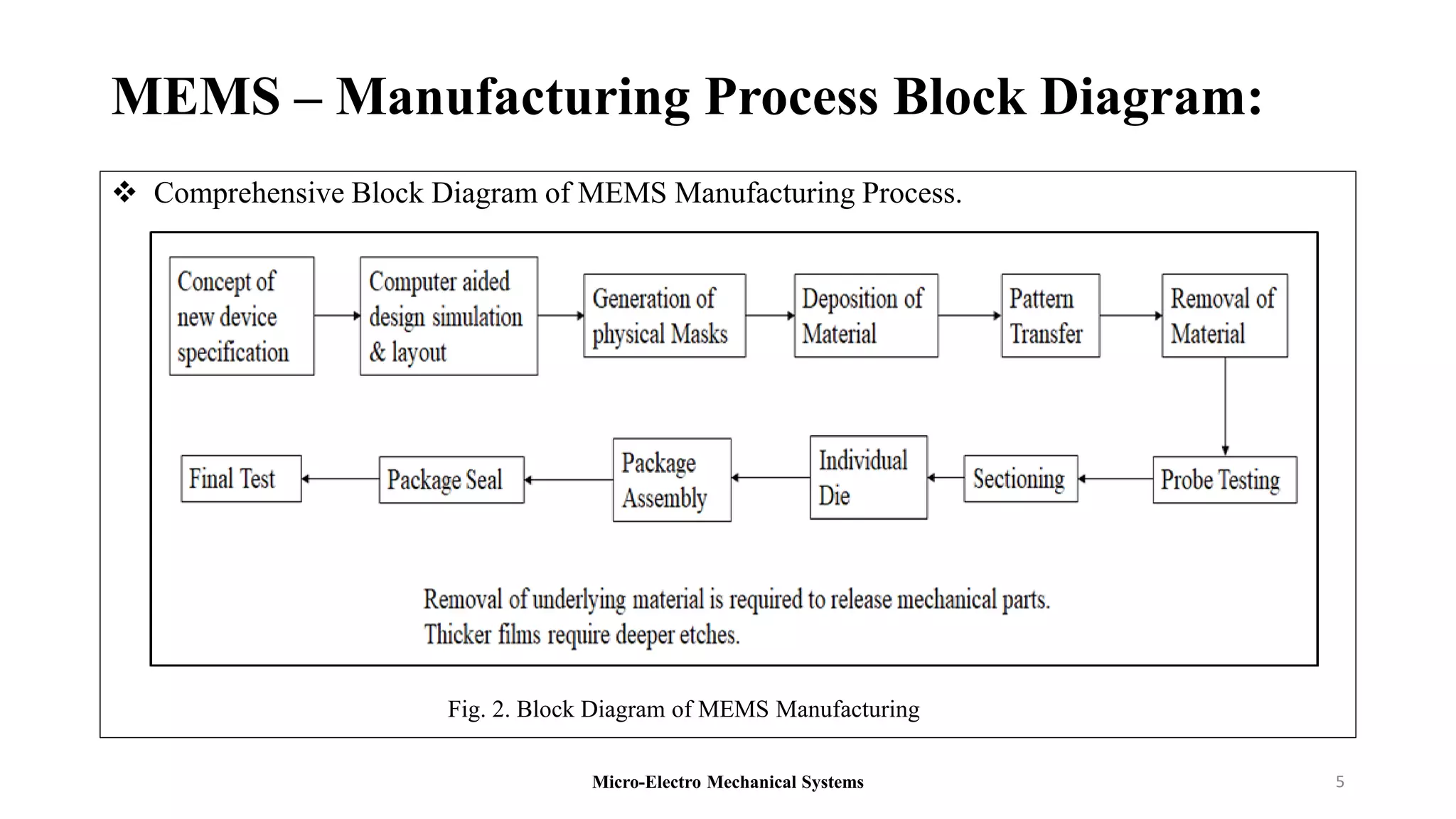
Overview of MEMS manufacturing processes through a block diagram illustrating the steps involved.
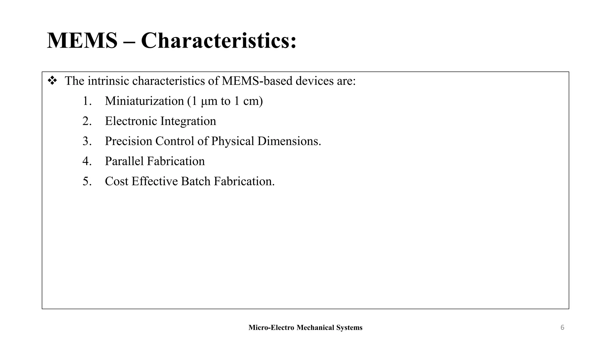
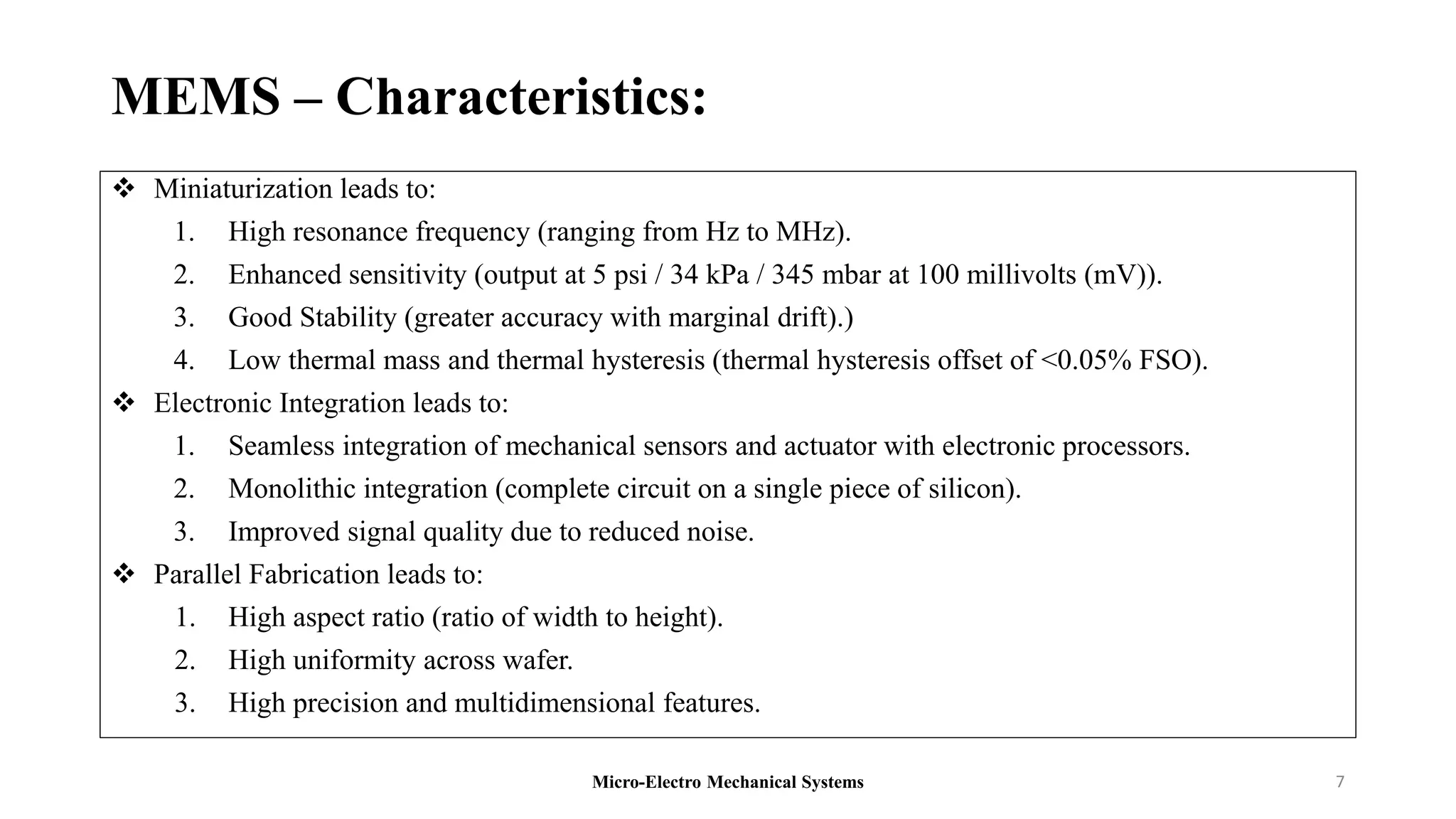
Key characteristics like miniaturization, electronic integration, and precision in MEMS devices.
Information on the miniaturized size of MEMS devices, their power consumption, and scale influence.
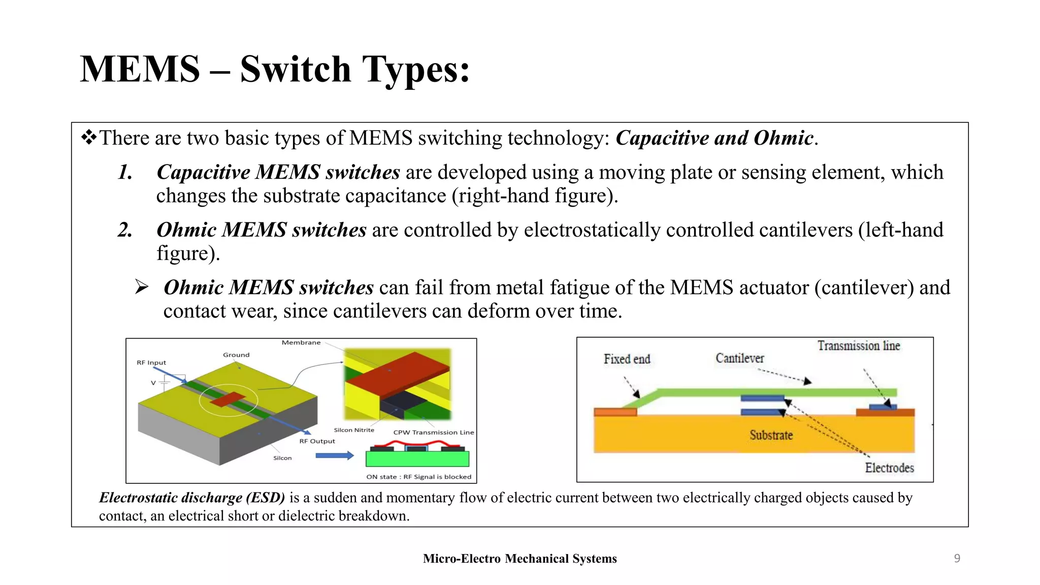
Two types of MEMS switches: capacitive and ohmic, including their operational mechanisms and challenges.
Discussion of benefits like small size, low power consumption, high productivity, and integration ease.
Drawbacks include power transfer challenges, material limitations, and reliability concerns.
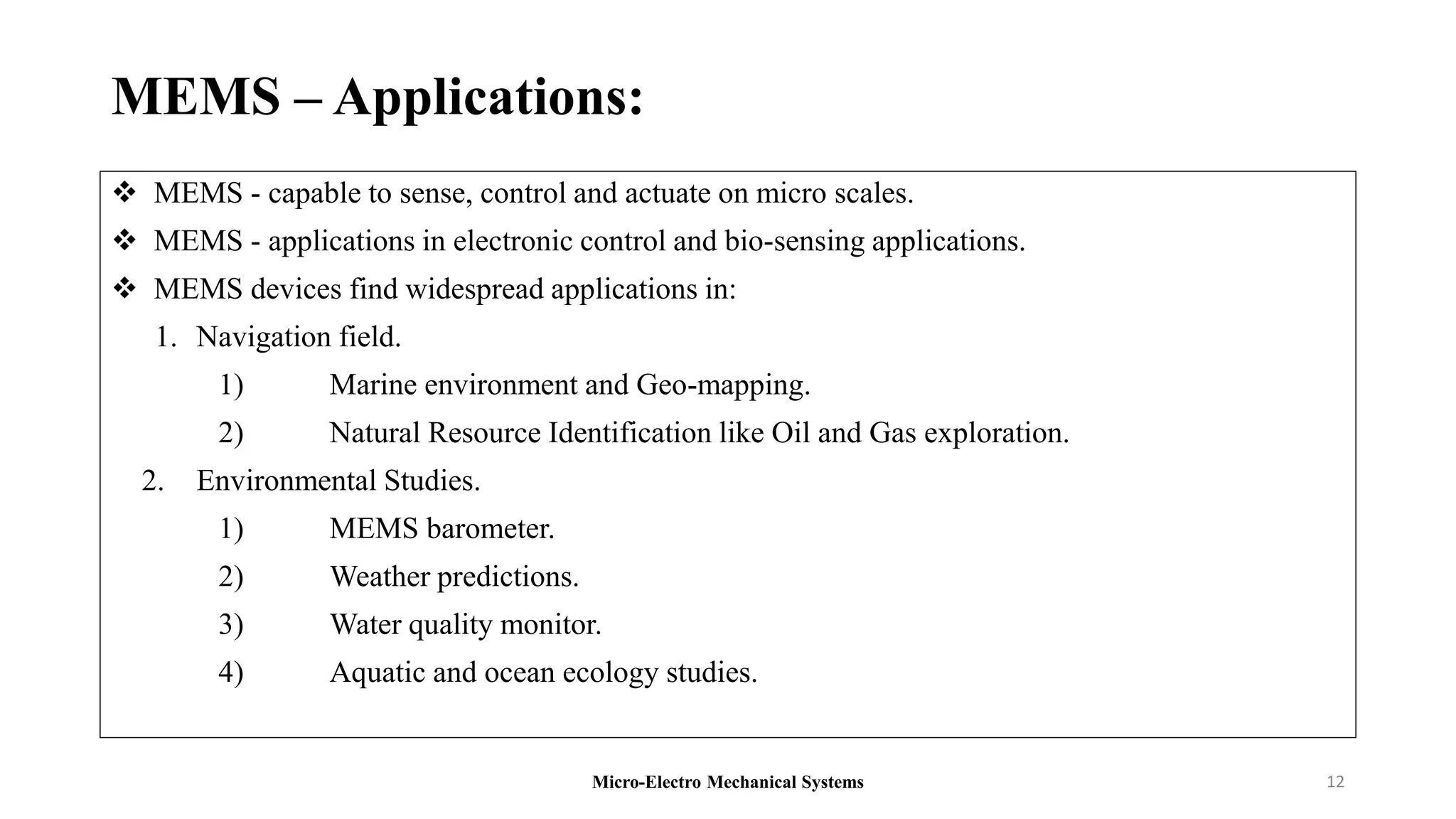
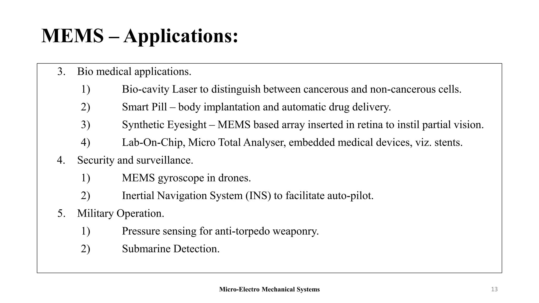
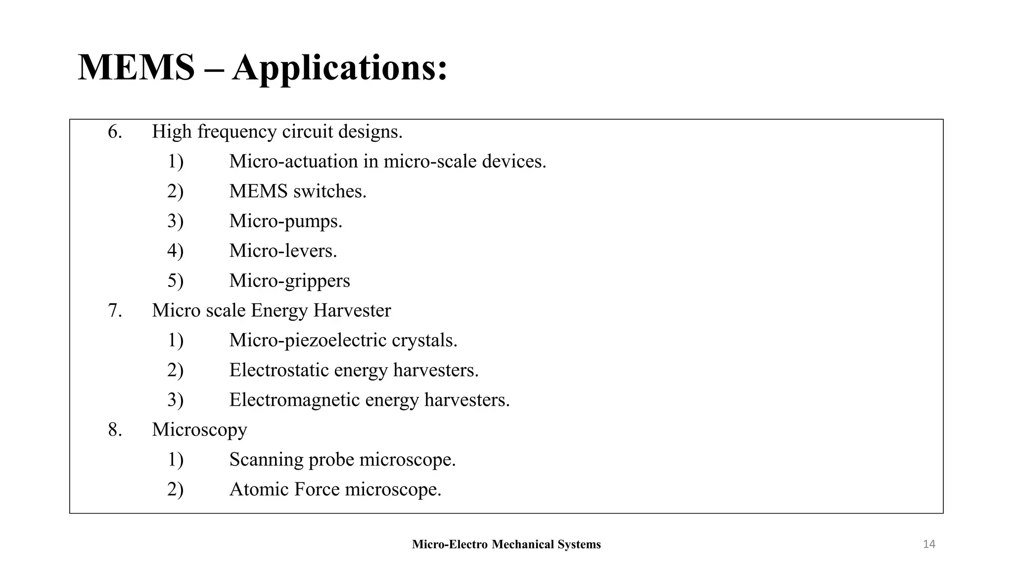
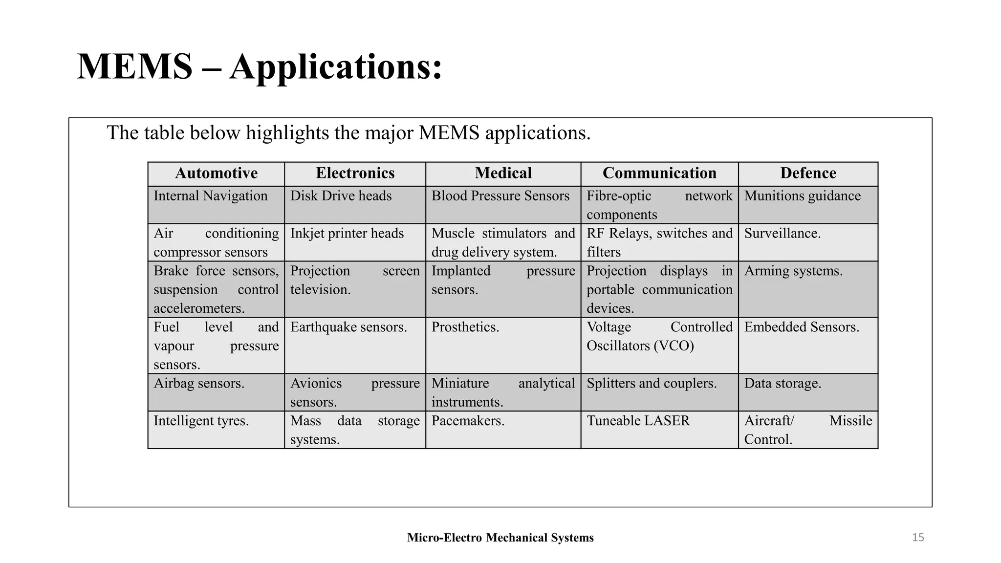
Diverse applications of MEMS in fields like navigation, environmental monitoring, medical devices, and more.
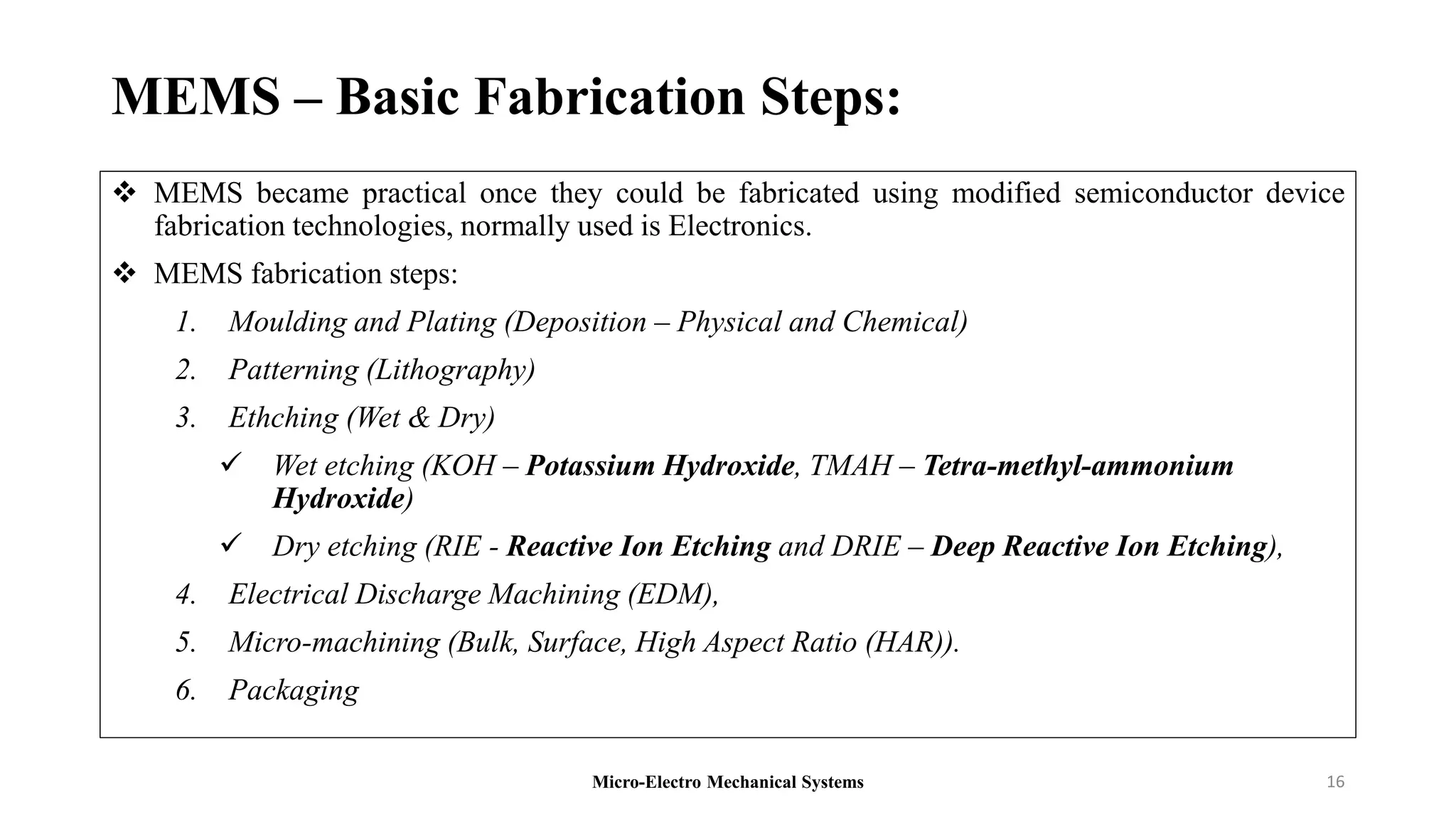
Outline of MEMS fabrication steps using semiconductor technologies including molding and lithography.
List of references and sources related to MEMS technologies and their applications.