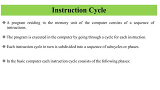
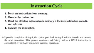
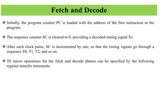
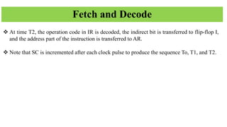
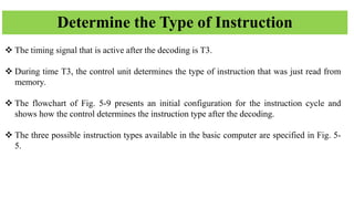
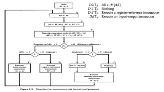
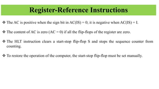
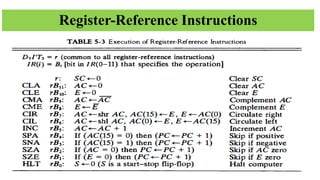
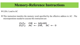
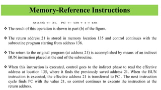
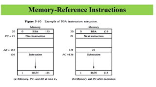
The document describes the instruction cycle process in a computer. It is divided into phases: fetch, decode, execute. Each instruction goes through this cycle. The phases are further divided into subcycles where the control unit determines the instruction type (register, memory, I/O), then performs the appropriate operations like fetching from memory, arithmetic/logic operations, and branching. Memory instructions include AND, ADD, LOAD, BRANCH etc. Register instructions modify registers directly. Subroutines are implemented using branch-and-save and indirect branch instructions.
The document summarizes the instruction cycle of a basic computer. It consists of four phases: 1) fetch instruction from memory, 2) decode instruction, 3) read effective address from memory if needed, 4) execute instruction. It then describes the fetch and decode phases in more detail using register transfer statements. Finally, it discusses the different types of instructions - register-reference and memory-reference - and provides examples of specific instructions like AND, ADD, LDA, STA, BUN, BSA, and ISZ.
The document describes the instruction cycle and execution of different types of instructions in a basic computer system. It discusses the fetch-decode-execute cycle that each instruction goes through. It then describes the three main types of instructions - memory reference instructions, register reference instructions, and input/output instructions. For each type, it provides examples and explains the steps in their execution cycles. It also covers program interrupts and how the computer handles interrupt requests from I/O devices.
This document discusses hardwired control and microprogrammed control in computer processors. It provides details on:
- Hardwired control generates control signals using logic circuits like gates and counters. It can operate at high speed but has little flexibility and complexity is limited.
- Microprogrammed control stores sequences of control words (microinstructions) in a control store. It uses a microprogram counter to sequentially fetch microinstructions and generate control signals. This allows for more flexible control but is slower than hardwired.
- Key components of a microprogrammed control unit include the control store, microprogram counter, and starting address generator block to load addresses and support conditional branching in the microcode.
The document discusses the timing and control, and instruction cycle of a basic computer. It contains the following key points:
1. The timing of all registers is controlled by a master clock generator which provides clock pulses to flip-flops and registers. Control signals are generated in the control unit to provide inputs for operations.
2. There are two types of control organization: hardwired and microprogrammed. Microprogrammed control stores control information in a control memory.
3. An instruction cycle consists of fetching an instruction from memory, decoding it, reading the effective address if indirect, and executing the instruction before fetching the next one. The program counter loads the first instruction address.
material for studentbasic computer organization and design .pptxjainyshah20
This document provides information about the basic components and organization of a computer. It discusses topics that will be covered, including instruction codes, registers, instructions, timing and control, memory-referenced instructions, input/output, and the design of basic computer components. It describes instruction codes and formats, including operation codes and direct vs indirect addressing. It outlines the major computer registers used including the program counter, instruction register, address register, and data registers. It also describes the types of basic computer instructions and the completeness of an instruction set. Finally, it provides details on the control unit and timing signals that coordinate the instruction cycle.
This document discusses the fundamental concepts and organization of the central processing unit (CPU). It describes how the CPU fetches, decodes, and executes instructions through a multi-step process. It explains that the CPU uses a program counter to keep track of the next instruction, and increments it after fetching and decoding each one. It also details how the CPU performs operations like fetching data from memory, storing to memory, transferring between registers, and performing arithmetic/logic functions using the ALU.
The document discusses input-output devices and interrupt handling in a computer system. It describes:
1) How input from devices like keyboards is received through an input register and output to devices like printers is sent through an output register.
2) How interrupt handling works, with an interrupt flip-flop getting set when input or output flags are raised, causing the computer to save its return address and branch to an interrupt service program.
3) The interrupt cycle in more detail, explaining how the return address is stored and how the computer returns to the main program after servicing the interrupt.
The microcontroller CPU has a 12-bit instruction set with 3 types of instructions encoded differently. It contains registers like the program counter, accumulator, and status register. The CPU uses a program memory to store instructions and a data memory for operands. It executes instructions in 3 stages - fetch, decode, execute. In each stage, control signals determine which components are enabled to perform operations like fetching instructions, reading operands, and executing ALU operations.
The document discusses computer instruction formats and addressing modes. It provides details on:
- Instruction codes contain operation codes and addresses to specify operations and memory/register locations.
- There are two addressing modes - direct addressing uses the operand's address while indirect uses a pointer.
- A basic instruction format has 12 bits for the address, 1 bit for the mode, and 3 bits for the operation code.
- An instruction cycle has four phases - fetch, decode, read effective address, and execute the instruction.
This document summarizes the instruction cycle of a CPU. It includes:
1) The main phases of the instruction cycle are fetch, decode, decision, and execute. It describes what happens in each phase, such as fetching the instruction from memory into the instruction register.
2) It describes the main circuits used in the CPU, including the program counter, memory address register, instruction register, and control unit.
3) It provides the details of the fetch, decode, and decision cycles in transfer notation, describing the step-by-step process and data flow between components like program counter and address register.
Computer organization involves fetching instructions from memory and executing them. There are two main approaches to implementing the control unit: hardwired control and microprogrammed control. Hardwired control uses combinational logic to generate control signals based on the instruction and state, while microprogrammed control stores control sequences as microinstructions in a separate control store.
I am working as a Assistant Professor in ITS, Ghaziabad. This is very useful to U.P.Technical University,Uttrakhand Technical University students. Give feedback to friendly_rakesh2003@yahoo.co.in
The document discusses the basic components and organization of a computer's instruction code and control unit.
1. An instruction code contains an operation code that defines the computer operation to perform, such as add or subtract, and operands that specify the data.
2. A computer's control unit decodes the instruction code and generates timing signals to control the execution of each instruction. It uses a sequence counter, decoders, and control logic gates.
3. The control unit increments the sequence counter on each clock cycle to produce the timing signals, or resets it based on the decoder outputs to control the execution sequence.
This document provides information on basic processing units. It discusses how the processor fetches and executes instructions one at a time by incrementing the program counter. Key registers like the instruction register and program counter are explained. The basic phases of fetching an instruction from memory and executing it are described. Concepts like register transfers, performing arithmetic/logic operations, and fetching data from memory are summarized. Important exam topics related to control units, branch instructions, and multiple bus organizations are highlighted.
Switch Control and Time Delay
1. LEDs and switches
2. Keypad and LEDs
3. Keypad and 8-segment LED C language and Assembly Code for Freescale MC9S08AW60
UNIT 5 Interfacing and Mixed Signal Controller.pptxGowrishankar C
The document discusses various programming concepts for interfacing microcontrollers including 8051 timers, serial communication, interrupts, keyboard, LCD, ADC, DAC, sensors, external memory, stepper motors, and waveform generation.
It describes how to program the 8051 timers in modes 1 and 2, including loading values, starting/stopping timers, and monitoring flags. It also discusses serial port, external interrupt, and timer interrupt programming. Other topics covered include procedures for interfacing keyboards, LCDs, ADCs, DACs, sensors, external memory, stepper motors, and generating waveforms like sine waves on the 8051.
This document provides information on programming timers, counters, serial communication, interrupts, and interfacing with various peripherals in 8051 microcontrollers. It describes the modes, registers, and procedures for programming timers in 8051. It also discusses programming serial communication, external interrupts, keyboard, LCD, and ADC interfacing with 8051 microcontrollers.
The CPU is divided into an arithmetic logic unit (ALU) and a control unit (CU). The CU generates timing and control signals to coordinate the flow of data between the CPU, memory, and peripherals. It directs the entire computer system to carry out instructions by communicating with the ALU and memory. The CU instructs the ALU on which operations to perform and coordinates all computer components. The CU can use either a hardwired or microprogrammed organization to generate control signals. A microprogrammed CU implements control through a program of microinstructions stored in control memory.
1. The document discusses the topics of computer instructions, timing and control, and the instruction cycle for a basic computer.
2. It describes the three instruction code formats used - memory reference, register reference, and input/output. Memory reference instructions use bits to specify an address and addressing mode. Register reference instructions specify an operation on the accumulator register.
3. The instruction cycle consists of four phases - fetch an instruction, decode the instruction, read the effective address if needed, and execute the instruction.
This document describes experiments with interfacing a microcontroller to a character LCD. It is divided into three parts: 1) Displaying a single letter on the LCD, 2) Displaying a string of characters, and 3) Shifting a message left and right continuously. The author explains the LCD module features and registers. Algorithms and flowcharts are provided for writing bytes to the LCD by first checking the busy flag and then sending command or data. Displaying a single letter "A" is achieved by writing the character data to the specified LCD coordinate.
The document discusses seven different memory reference instructions used in a computer system. The instructions include AND to AC, ADD to AC, LDA, STA, BUN, BSA, and ISZ. Each instruction requires a sequence of microoperations to read data from memory into a register, perform the operation, and update registers or memory. For example, the LDA instruction reads the memory word specified by the effective address into the data register in T4, then transfers this value to the accumulator in T5 before clearing the sequence counter.
This document describes interfacing an LCD display and keyboard to an 8051 microcontroller. It discusses connecting the LCD to output pins of the microcontroller to control the display. Commands are sent to initialize and update the LCD. A similar process of scanning rows and columns is used to interface a 4x4 keyboard matrix and detect which key is pressed by checking for a closed row and column. The document provides code examples to write characters to the LCD and scan the keyboard to identify pressed keys.
Introduction to 8085 & it's description(includes basic lab experiments)Basil John
The document provides information about the 8085 microprocessor. It describes the 8085 as an 8-bit microprocessor capable of addressing 64KB of memory. It then details the various functional blocks of the 8085 including general purpose registers, accumulator, program counter, stack pointer, ALU, flags register, timing and control unit, and instruction register and decoder. Finally, it provides examples of assembly language programs for 8-bit addition, subtraction, and 16-bit addition and subtraction on the 8085 microprocessor.
This document describes instruction codes and the instruction cycle in a computer. It discusses how instruction codes specify operations for the computer to perform. The instruction cycle has four phases: 1) fetch an instruction from memory, 2) decode the instruction, 3) read the effective address if indirect addressing is used, and 4) execute the instruction. It then describes the fetch and decode phases in more detail, including transferring the program counter value to the address register to fetch the instruction from memory location and loading the instruction register.
basic computer programming and micro programmed controlRai University
- The document discusses basic computer programming concepts and their relation to hardware representation of instructions. It introduces instruction sets, machine language, assembly language, and the translation process from symbolic to binary code using an assembler.
- The assembler performs two passes: the first generates an address symbol table by assigning memory locations to labels and operands, and the second translates the symbolic code to binary using lookup tables for instructions, operands, and the address symbol table.
- Assembly language allows the use of symbolic names for instructions, addresses, and operands, making programs more human-readable compared to binary or machine language.
Mca i-u-3-basic computer programming and micro programmed controlRai University
This document discusses basic computer programming and microprogrammed control. It introduces some basic programming concepts and their relation to hardware representation of instructions. It describes how a program may be dependent or independent of the computer that runs it. It also discusses machine language, assembly language, and the translation process from symbolic code to binary code using an assembler. Examples are provided of assembly language programs for addition and multiplication.
The document discusses interfacing a microcontroller with various peripherals including timers, serial communication, interrupts, LCDs, and keyboards. It provides details on:
- Programming timers in 8051 microcontrollers for time delays and waveform generation.
- Serial communication protocols including asynchronous communication and RS-232 standards.
- Configuring and handling interrupts from different sources and writing interrupt service routines.
- Interfacing 8051 with LCDs for display and matrix keyboards for input using specific I/O ports for scanning rows and columns.
The Building Blocks of QuestDB, a Time Series Databasejavier ramirez
Talk Delivered at Valencia Codes Meetup 2024-06.
Traditionally, databases have treated timestamps just as another data type. However, when performing real-time analytics, timestamps should be first class citizens and we need rich time semantics to get the most out of our data. We also need to deal with ever growing datasets while keeping performant, which is as fun as it sounds.
It is no wonder time-series databases are now more popular than ever before. Join me in this session to learn about the internal architecture and building blocks of QuestDB, an open source time-series database designed for speed. We will also review a history of some of the changes we have gone over the past two years to deal with late and unordered data, non-blocking writes, read-replicas, or faster batch ingestion.
Learn SQL from basic queries to Advance queriesmanishkhaire30
Dive into the world of data analysis with our comprehensive guide on mastering SQL! This presentation offers a practical approach to learning SQL, focusing on real-world applications and hands-on practice. Whether you're a beginner or looking to sharpen your skills, this guide provides the tools you need to extract, analyze, and interpret data effectively.
Key Highlights:
Foundations of SQL: Understand the basics of SQL, including data retrieval, filtering, and aggregation.
Advanced Queries: Learn to craft complex queries to uncover deep insights from your data.
Data Trends and Patterns: Discover how to identify and interpret trends and patterns in your datasets.
Practical Examples: Follow step-by-step examples to apply SQL techniques in real-world scenarios.
Actionable Insights: Gain the skills to derive actionable insights that drive informed decision-making.
Join us on this journey to enhance your data analysis capabilities and unlock the full potential of SQL. Perfect for data enthusiasts, analysts, and anyone eager to harness the power of data!
#DataAnalysis #SQL #LearningSQL #DataInsights #DataScience #Analytics
The Ipsos - AI - Monitor 2024 Report.pdfSocial Samosa
According to Ipsos AI Monitor's 2024 report, 65% Indians said that products and services using AI have profoundly changed their daily life in the past 3-5 years.
ViewShift: Hassle-free Dynamic Policy Enforcement for Every Data LakeWalaa Eldin Moustafa
Dynamic policy enforcement is becoming an increasingly important topic in today’s world where data privacy and compliance is a top priority for companies, individuals, and regulators alike. In these slides, we discuss how LinkedIn implements a powerful dynamic policy enforcement engine, called ViewShift, and integrates it within its data lake. We show the query engine architecture and how catalog implementations can automatically route table resolutions to compliance-enforcing SQL views. Such views have a set of very interesting properties: (1) They are auto-generated from declarative data annotations. (2) They respect user-level consent and preferences (3) They are context-aware, encoding a different set of transformations for different use cases (4) They are portable; while the SQL logic is only implemented in one SQL dialect, it is accessible in all engines.
#SQL #Views #Privacy #Compliance #DataLake
Global Situational Awareness of A.I. and where its headedvikram sood
You can see the future first in San Francisco.
Over the past year, the talk of the town has shifted from $10 billion compute clusters to $100 billion clusters to trillion-dollar clusters. Every six months another zero is added to the boardroom plans. Behind the scenes, there’s a fierce scramble to secure every power contract still available for the rest of the decade, every voltage transformer that can possibly be procured. American big business is gearing up to pour trillions of dollars into a long-unseen mobilization of American industrial might. By the end of the decade, American electricity production will have grown tens of percent; from the shale fields of Pennsylvania to the solar farms of Nevada, hundreds of millions of GPUs will hum.
The AGI race has begun. We are building machines that can think and reason. By 2025/26, these machines will outpace college graduates. By the end of the decade, they will be smarter than you or I; we will have superintelligence, in the true sense of the word. Along the way, national security forces not seen in half a century will be un-leashed, and before long, The Project will be on. If we’re lucky, we’ll be in an all-out race with the CCP; if we’re unlucky, an all-out war.
Everyone is now talking about AI, but few have the faintest glimmer of what is about to hit them. Nvidia analysts still think 2024 might be close to the peak. Mainstream pundits are stuck on the wilful blindness of “it’s just predicting the next word”. They see only hype and business-as-usual; at most they entertain another internet-scale technological change.
Before long, the world will wake up. But right now, there are perhaps a few hundred people, most of them in San Francisco and the AI labs, that have situational awareness. Through whatever peculiar forces of fate, I have found myself amongst them. A few years ago, these people were derided as crazy—but they trusted the trendlines, which allowed them to correctly predict the AI advances of the past few years. Whether these people are also right about the next few years remains to be seen. But these are very smart people—the smartest people I have ever met—and they are the ones building this technology. Perhaps they will be an odd footnote in history, or perhaps they will go down in history like Szilard and Oppenheimer and Teller. If they are seeing the future even close to correctly, we are in for a wild ride.
Let me tell you what we see.
Global Situational Awareness of A.I. and where its headed
11. Lecture.pdf
1. Instruction Cycle
❖ A program residing in the memory unit of the computer consists of a sequence of
instructions.
❖ The program is executed in the computer by going through a cycle for each instruction.
❖ Each instruction cycle in turn is subdivided into a sequence of subcycles or phases.
❖ In the basic computer each instruction cycle consists of the following phases:
2. Instruction Cycle
❖ Upon the completion of step 4, the control goes back to step 1 to fetch, decode, and execute
the next instruction. This process continues indefinitely unless a HALT instruction is
encountered. {The HALT instruction suspends operations}
3. Fetch and Decode
❖ Initially, the program counter PC is loaded with the address of the first instruction in the
program.
❖ The sequence counter SC is cleared to 0, providing a decoded timing signal To.
❖ After each clock pulse, SC is incremented by one, so that the timing signals go through a
sequence T0, T1, T2, and so on.
❖ Th rnicro operations for the fetch and decode phases can be specified by the following
register transfer statements.
4. Fetch and Decode
❖ Since only AR is connected to the address inputs of memory, it is necessary to transfer the
address from PC to AR during the clock transition associated with timing signal T0.
❖ The instruction read from memory is then placed in the instruction register IR with the
clock transition associated with timing signal T1.
❖ At the same time, PC is incremented by one to prepare it for the address of the next
instruction in the program.
5. Fetch and Decode
❖ At time T2, the operation code in IR is decoded, the indirect bit is transferred to flip-flop I,
and the address part of the instruction is transferred to AR.
❖ Note that SC is incremented after each clock pulse to produce the sequence To, T1, and T2.
6. Fetch and Decode
❖ Figure 5-8 shows how the first two register transfer statements are implemented in the bus
system.
❖ To provide the data path for the transfer of PC to AR we must apply timing signal T0 to
achieve the following connection:
❖ 1. Place the content of PC onto the bus by making the bus selection inputs S2S1S0 equal to
010.
❖ 2. Transfer the content of the bus to AR by enabling the LD input of AR .
7. Fetch and Decode
❖ The next clock transition initiates the transfer from PC to AR since T0 = 1. In order to
implement the second statement.
8. Fetch and Decode
❖ The next clock transition initiates the read and increment operations since T, = 1 .
❖ Figure 5-8 duplicates a portion o f the bus system and shows how T0 and T1, are connected
to the control inputs of the registers, the memory, and the bus selection inputs.
❖ Multiple input OR gates are included in the diagram because there are other control
functions that will initiate similar operations.
10. Determine the Type of Instruction
❖ The timing signal that is active after the decoding is T3.
❖ During time T3, the control unit determines the type of instruction that was just read from
memory.
❖ The flowchart of Fig. 5-9 presents an initial configuration for the instruction cycle and
shows how the control determines the instruction type after the decoding.
❖ The three possible instruction types available in the basic computer are specified in Fig. 5-
5.
13. Determine the Type of Instruction
❖ Decoder output D, is equal to 1 if the operation code is equal to binary 111.
❖ From Fig. 5-5 we determine that if D7 = 1, the instruction must be a register-reference or
input-output type.
❖ If D7, = 0, the operation code must be one of the other seven values 000 through 110,
specifying a memory-reference instruction.
❖ Control then inspects the value of the first bit of the instruction, which is now available in
flip-flop I. If D7 = 0 and I = 1, we have a memory reference instruction with an indirect
address.
14. Determine the Type of Instruction
❖ effective address from memory. The microoperation for the indirect address condition can
be symbolized by the register transfer statement
❖ Initially, AR holds the address part of the instruction.
❖ This address is used during the memory read operation.
❖ The word at the address given by AR is read from memory and placed on the common bus.
❖ The LD input of AR is then enabled to receive the indirect address that resided in the 12
least significant bits of the memory word.
17. Register-Reference Instructions
❖ Register-reference instructions are recognized by the control when D7 = 1 and I = 0.
❖ These instructions use bits 0 through 11 of the instruction code to specify one of 12
instructions. These 12 bits are available in IR(0-11).
❖ They were also transferred to AR during time T2.
18. Register-Reference Instructions
❖ The control functions and microoperations for the register-reference are listed in Table 5-3.
❖ These instructions are executed with the clock transition associated with timing variable T3.
❖ Each control function needs the Boolean relation D7I' T3, which we designate for
convenience by the symbol r .
❖ The control function is distinguished by one o f the bits in IR(0-11). By assigning the
symbol Bi, to bit i of IR, all control functions can be simply denoted by rBi.
19. Register-Reference Instructions
❖ For example, the instruction CLA has the hexadecimal code 7800 (see Table 5-2), which
gives the binary equivalent 01 1 1 1000 0000 0000. The first bit is a zero and is equivalent
to I ‘ .
❖ The next three bits constitute the operation code and are recognized from decoder output
D7. Bit 11 in IR is 1 and is recognized from B11.
❖ The control function that initiates the microoperation for this instruction is
❖ D7I ' T3 B11 = rB11.
❖ The execution of a register-reference instruction is completed at time T3. The sequence
counter SC is cleared to 0 and the control goes back to fetch the next instruction with
timing signal T0.
20. Register-Reference Instructions
❖ The first seven register-reference instructions perform clear, complement, circular shift, and
increment micro-operations on the AC or E registers.
❖ The next four instructions cause a skip of the next instruction in sequence when a stated
condition is satisfied.
❖ The skipping of the instruction is achieved by incrementing PC once again (in addition, it is
being incremented during the fetch phase at time T1).
❖ The condition control statements must be recognized as part of the control conditions.
21. Register-Reference Instructions
❖ The AC is positive when the sign bit in AC(IS) = 0; it is negative when AC(IS) = I.
❖ The content of AC is zero (AC = 0) if all the flip-flops of the register are zero.
❖ The HLT instruction clears a start-stop flip-flop S and stops the sequence counter from
counting.
❖ To restore the operation of the computer, the start-stop flip-flop must be set manually.
23. Memory-Reference Instructions
❖ Table 5-4 lists the seven memory-reference instructions.
❖ The decoded output D; for i = 0, 1, 2, 3, 4, 5, and 6 from the operation decoder that belongs
to each instruction is included in the table.
❖ The effective address of the instruction is in the address register AR and was placed there
during timing signal T2 when I = 0, or during timing signal T3 when I = 1.
❖ The execution of the memory-reference instructions starts with timing signal T4.
❖ The symbolic description of each instruction is specified in the table in terms of register
transfer notation.
25. Memory-Reference Instructions
❖ The actual execution of the instruction in the bus system will require a sequence of micro-
operations.
❖ This is because data stored in memory cannot be processed directly.
❖ The data must be read from memory to a register where they can be operated on with logic
circuits.
❖ We now explain the operation of each instruction and list the control functions and micro-
operations needed for their execution.
❖ A flowchart that summarizes all the microoperations is presented at the end of this section.
27. Memory-Reference Instructions
❖ AND to AC
❖ This is an instruction that performs the AND logic operation on pairs of bits in AC and the
memory word specified by the effective address.
❖ The result of the operation is transferred to AC.
❖ The microoperations that execute this instruction are:
28. Memory-Reference Instructions
❖ ADD to AC
❖ This instruction adds the content of the memory word specified by the effective address to
the value of AC .
❖ The sum is transferred into AC and the output carry Cout is transferred to the E (extended
accumulator) flip-flop.
❖ The microoperations needed to execute this instruction are
29. Memory-Reference Instructions
❖ The same two timing signals, T, and T5, are used again but with operation decoder D1
instead of D0, which was used for the AND instruction.
30. Memory-Reference Instructions
❖ LDA: Load to AC
❖ This instruction transfers the memory word specified by the effective address to AC . The
microoperations needed to execute this instruction are
32. Memory-Reference Instructions
❖ BUN: Branch Unconditionally
❖ This instruction transfers the program to the instruction specified by the effective address.
Remember that PC holds the address of the instruction to be read from memory in the next
instruction cycle.
❖ PC is incremented at time T1 to prepare it for the address of the next instruction in the
program sequence.
❖ The BUN instruction allows the programmer to specify an instruction out of sequence and
we say that the program branches (or jumps) unconditionally. The instruction is executed
with one microoperation:
34. Memory-Reference Instructions
❖ BSA: Branch and Save Return Address
❖ This instruction is useful for branching to a portion of the program called a subroutine or
procedure.
❖ When executed, the BSA instruction stores the address of the next instruction in sequence
(which is available in PC) into a memory location specified by the effective address.
❖ The effective address plus one is then transferred to PC to serve as the address of the first
instruction in the subroutine.
35. Memory-Reference Instructions
❖ A numerical example that demonstrates how this instruction is used with a subroutine is
shown in Fig. 5-10. The BSA instruction is assumed to be in memory at address 20.
❖ The I bit is 0 and the address part of the instruction has the binary equivalent of 135.
❖ After the fetch and decode phases, PC contains 21, which is the address of the next
instruction in the program (referred to as the return address).
❖ AR holds the effective address 135. This is shown in part (a) of the figure. The BSA
instruction performs the following numerical operation:
36. Memory-Reference Instructions
❖ The result of this operation is shown in part (b) of the figure.
❖ The return address 21 is stored in memory location 135 and control continues with the
subroutine program starting from address 136.
❖ The return to the original program (at address 21) is accomplished by means of an indirect
BUN instruction placed at the end of the subroutine.
❖ When this instruction is executed, control goes to the indirect phase to read the effective
address at location 135, where it finds the previously saved address 21. When the BUN
instruction is executed, the effective address 21 is transferred to PC . The next instruction
cycle finds PC with the value 21, so control continues to execute the instruction at the
return address.
37. Memory-Reference Instructions
❖ The BSA instruction performs the function usually referred to as a subroutine call.
❖ The indirect BUN instruction at the end of the subroutine performs the function referred to
as a subroutine return.
39. Memory-Reference Instructions
❖ To use the memory and the bus properly, the BSA instruction must be executed With a
sequence of two microoperations
❖ Timing signal T4 initiates a memory write operation, places the content of PC onto the bus,
and enables the INR input of AR .
❖ The memory write operation is completed and AR is incremented by the time the next clock
transition occurs. The bus is used at T5 to transfer the content of AR to PC .
40. Memory-Reference Instructions
❖ This instruction increments the word specified by the effective address, and if the
incremented value is equal to 0, PC is incremented by 1.