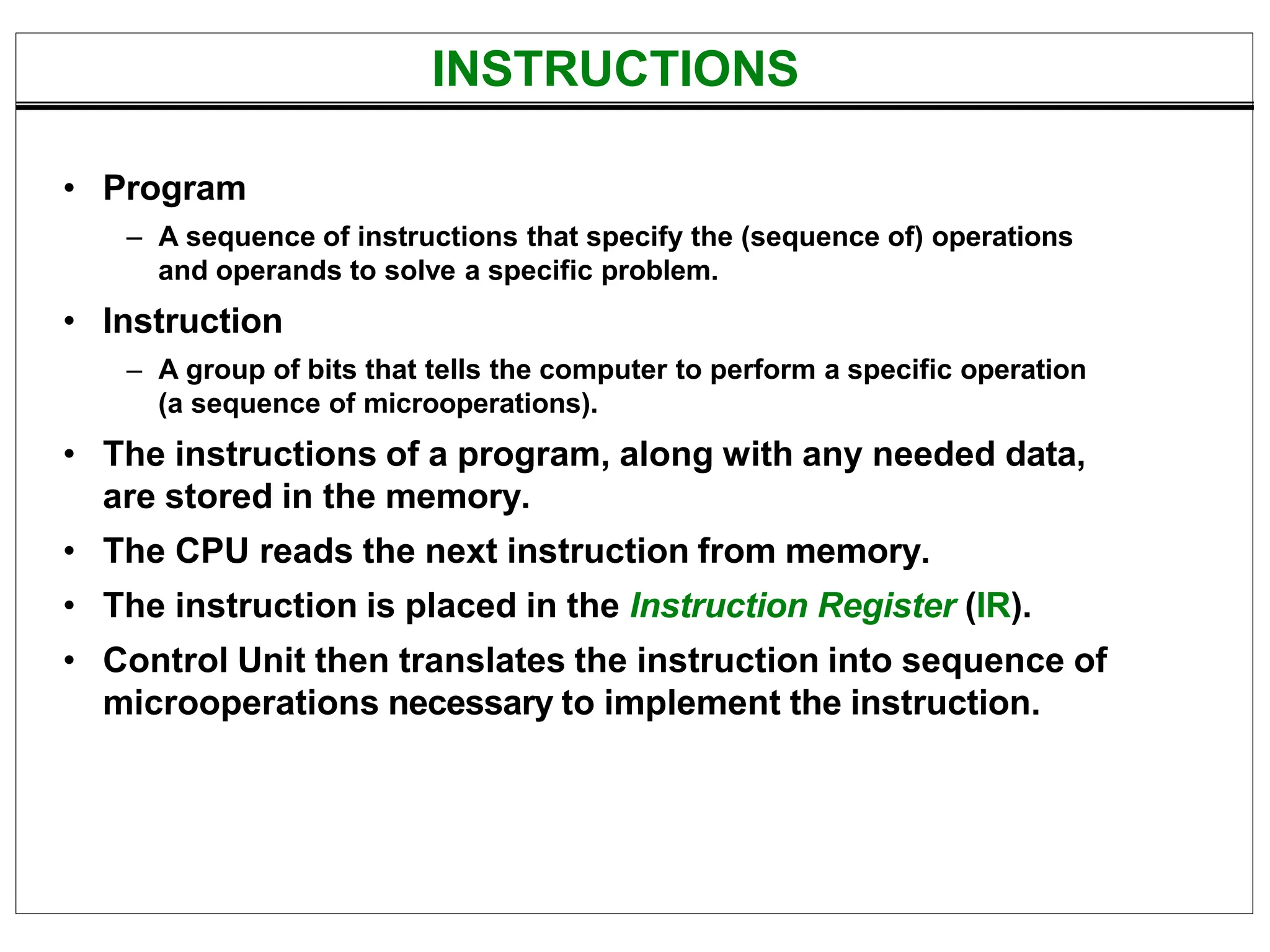
INSTRUCTIONS
• Program
– Asequence of instructions that specify the (sequence of) operations
and operands to solve a specific problem.
• Instruction
– A group of bits that tells the computer to perform a specific operation
(a sequence of microoperations).
• The instructions of a program, along with any needed data,
are stored in the memory.
• The CPU reads the next instruction from memory.
• The instruction is placed in the Instruction Register (IR).
• Control Unit then translates the instruction into sequence of
microoperations necessary to implement the instruction.
3.
INSTRUCTION CYCLE
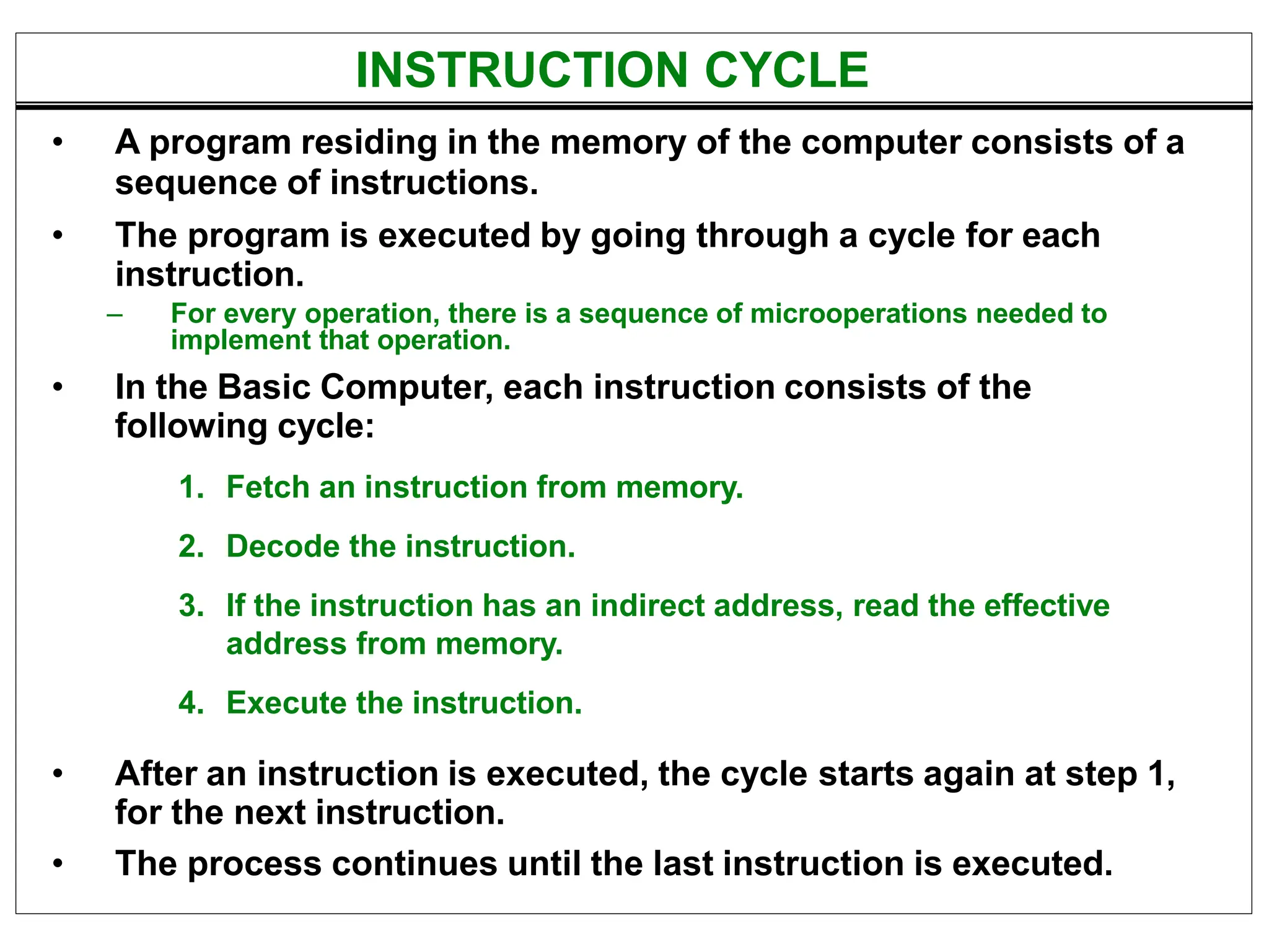
• Aprogram residing in the memory of the computer consists of a
sequence of instructions.
• The program is executed by going through a cycle for each
instruction.
– For every operation, there is a sequence of microoperations needed to
implement that operation.
• In the Basic Computer, each instruction consists of the
following cycle:
1. Fetch an instruction from memory.
2. Decode the instruction.
3. If the instruction has an indirect address, read the effective
address from memory.
4. Execute the instruction.
• After an instruction is executed, the cycle starts again at step 1,
for the next instruction.
• The process continues until the last instruction is executed.
4.
FETCH and DECODE
Fetchand Decode
T0: AR PC (S2S1S0 = 010, T0 = 1)
T1: IR M[AR], PC PC + 1 (S2S1S0 = 111, T1 = 1)
T2: D0, . . . , D7 Decode IR(12-14),AR IR(0-11), I IR(15)
S2
S1
S0
Bus
7
Memory
unit
AR
LD
PC
INR
IR
LD
Clock
1
2
5
Common bus
T1
T0
Address
Read
5.
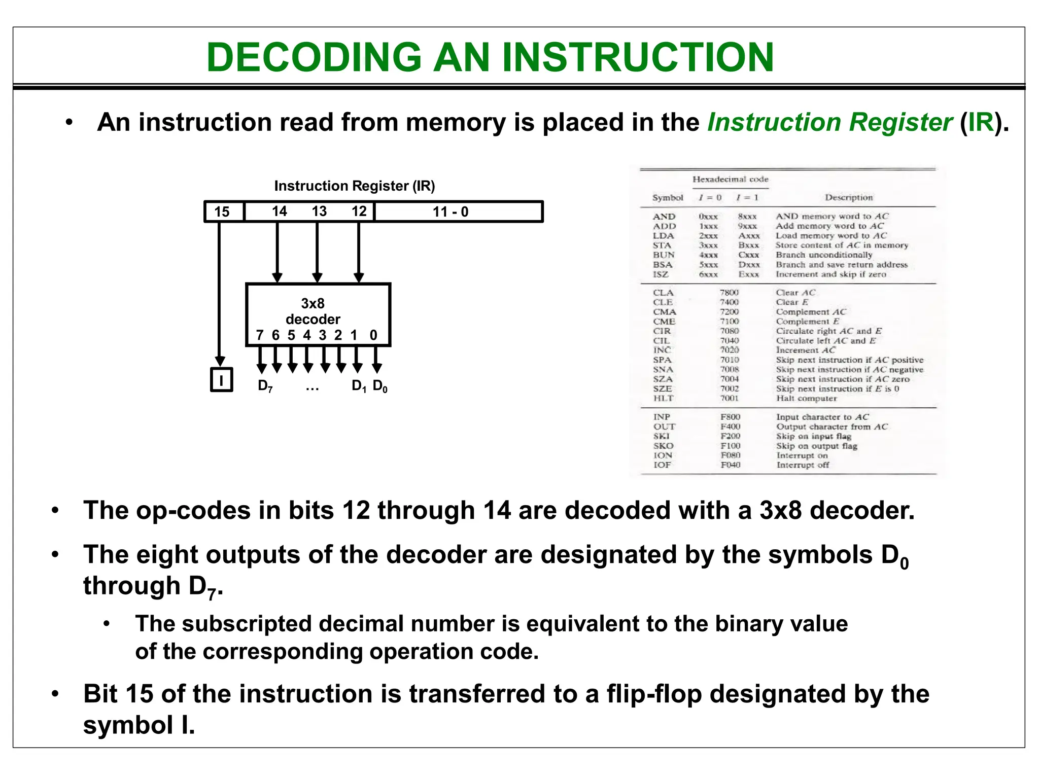
DECODING AN INSTRUCTION
InstructionRegister (IR)
15 14 13 12 11 - 0
3x8
decoder
7 6 5 4 3 2 1 0
I D7 … D1 D0
• An instruction read from memory is placed in the Instruction Register (IR).
• The op-codes in bits 12 through 14 are decoded with a 3x8 decoder.
• The eight outputs of the decoder are designated by the symbols D0
through D7.
• The subscripted decimal number is equivalent to the binary value
of the corresponding operation code.
• Bit 15 of the instruction is transferred to a flip-flop designated by the
symbol I.
DETERMINE THE TYPEOF INSTRUCTION
D7' I T3:
D7' I' T3:
D7 I' T3:
D7 I T3:
AR M[AR]
Nothing
Execute a Register-reference instruction
Execute an Input/Output instruction
Start
SC 0
= 0 (direct)
AR PC
T0
IR M[AR], PC PC + 1
T1
Decode op-code in IR(12-14),
AR IR(0-11), I IR(15)
T2
D7
= 0 (Memory-reference)
(Register or I/O) = 1
I
I
Execute
register-reference
instruction
SC 0
Execute
input/output
instruction
SC 0
AR M[AR] Nothing
= 0 (Register)
(I/O) = 1 (indirect) = 1
T3
Execute
memory-reference
instruction
SC 0
T4
T3 T3
T3
8.
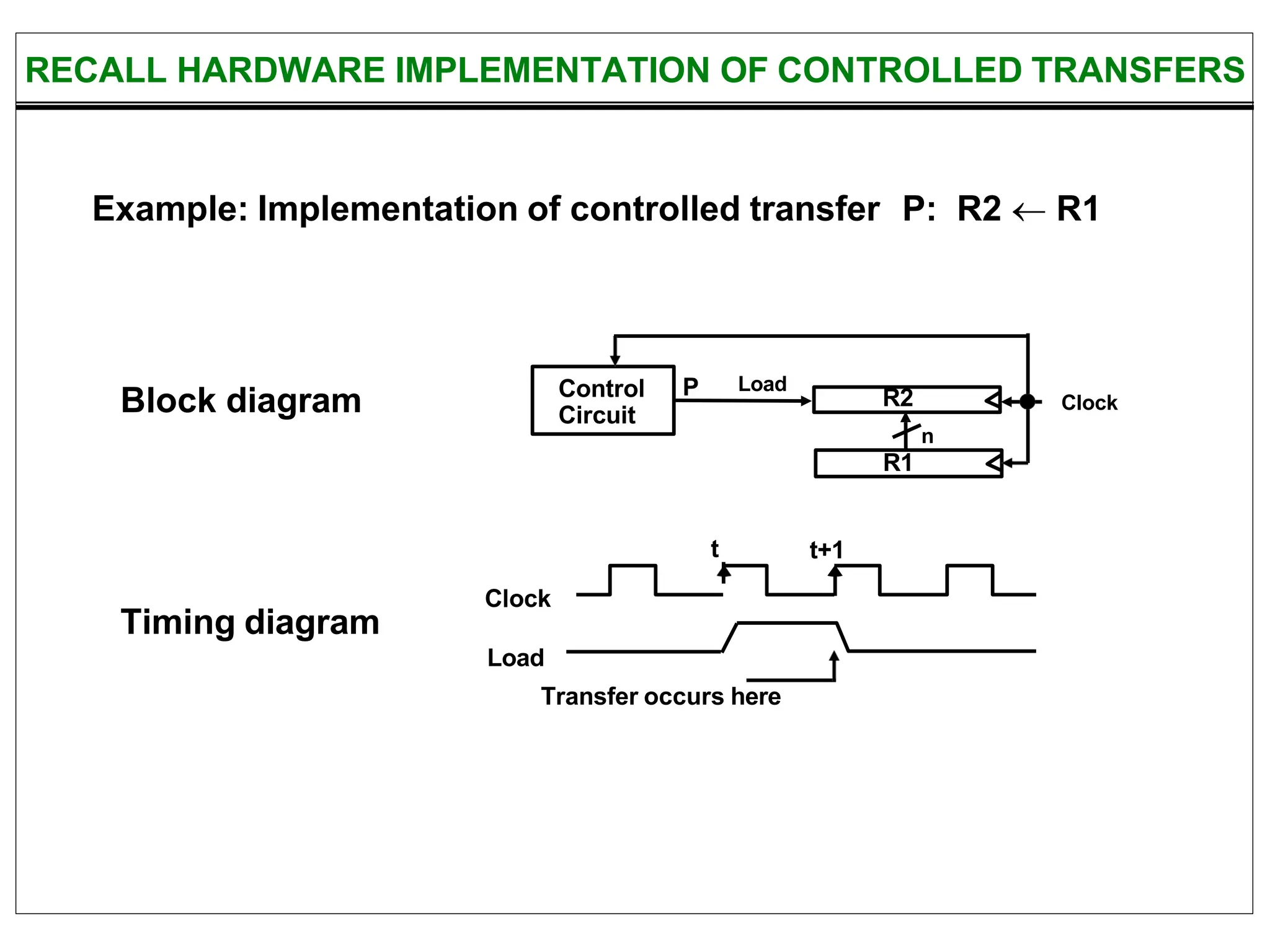
RECALL HARDWARE IMPLEMENTATIONOF CONTROLLED TRANSFERS
Example: Implementation of controlled transfer P: R2 R1
Block diagram
Timing diagram
Clock
R2
R1
Control
Circuit
Load
P
n
t t+1
Clock
Load
Transfer occurs here
9.
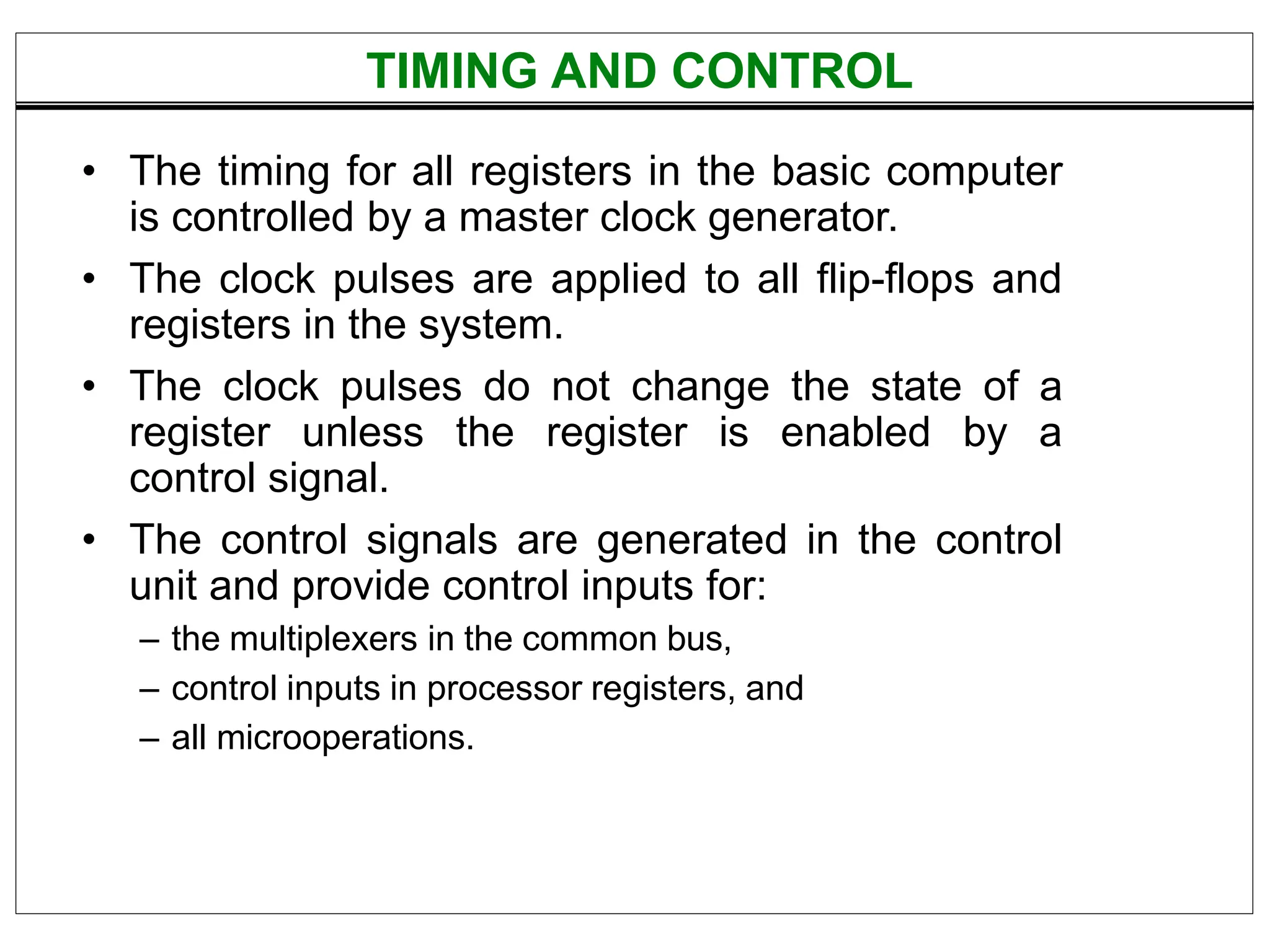
TIMING AND CONTROL
•The timing for all registers in the basic computer
is controlled by a master clock generator.
• The clock pulses are applied to all flip-flops and
registers in the system.
• The clock pulses do not change the state of a
register unless the register is enabled by a
control signal.
• The control signals are generated in the control
unit and provide control inputs for:
– the multiplexers in the common bus,
– control inputs in processor registers, and
– all microoperations.
10.
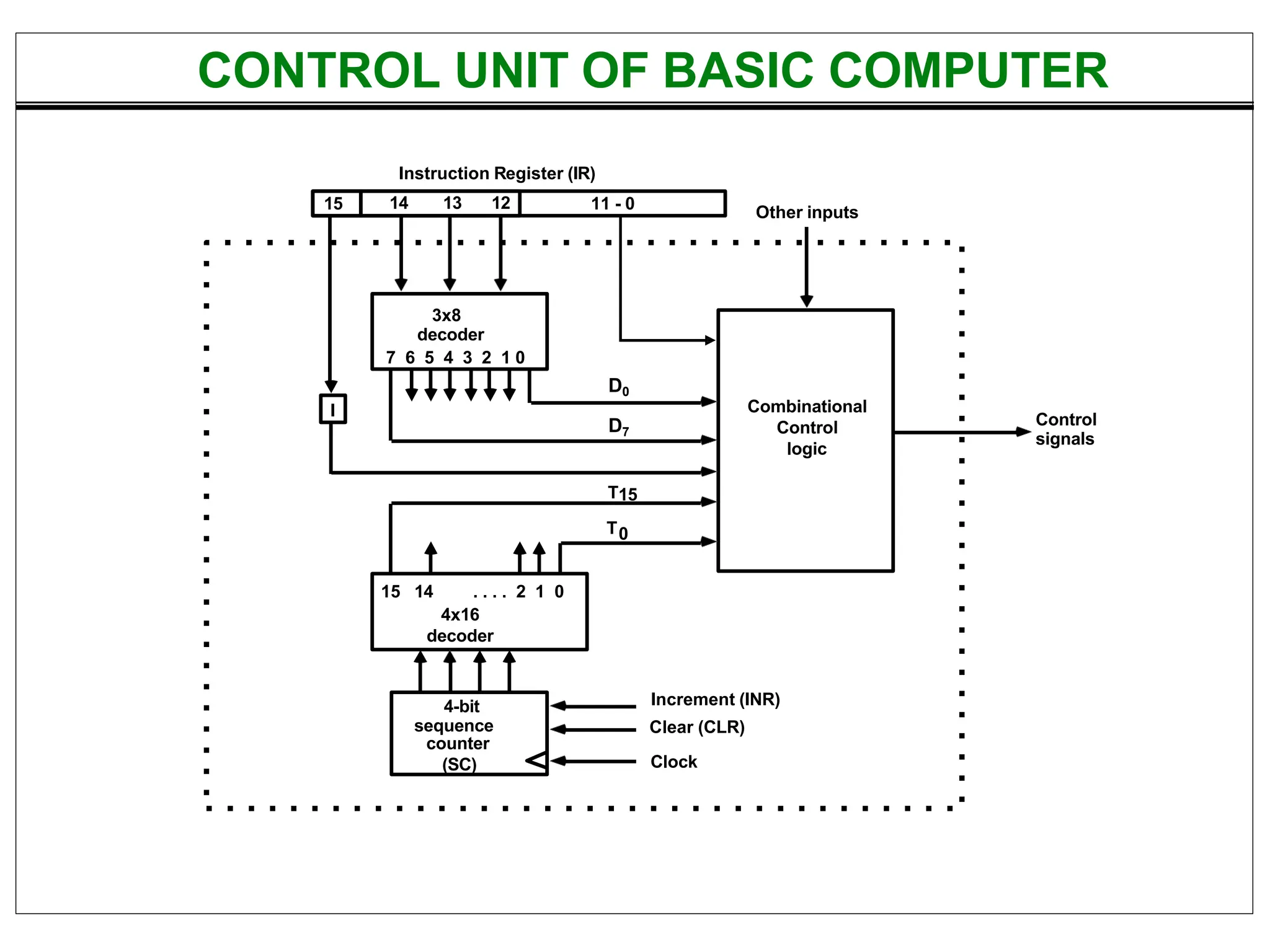
CONTROL UNIT OFBASIC COMPUTER
Instruction Register (IR)
15 14 13 12 11 - 0
3x8
decoder
7 6 5 4 3 2 1 0
I
D0
4-bit
sequence
counter
(SC)
Increment (INR)
Clear (CLR)
Clock
Other inputs
Control
signals
D7
T15
T0
15 14 . . . . 2 1 0
4x16
decoder
Combinational
Control
logic
• The SequenceCounter (SC) can be incremented or
cleared.
• Most of the time, the counter is incremented to provide
the sequence of timing signals out of the 4x16 decoder.
• Once in a while, the counter is cleared to 0, causing the
next active timing signal to be T0.
• The sequence counter responds to the positive
transition of the clock.
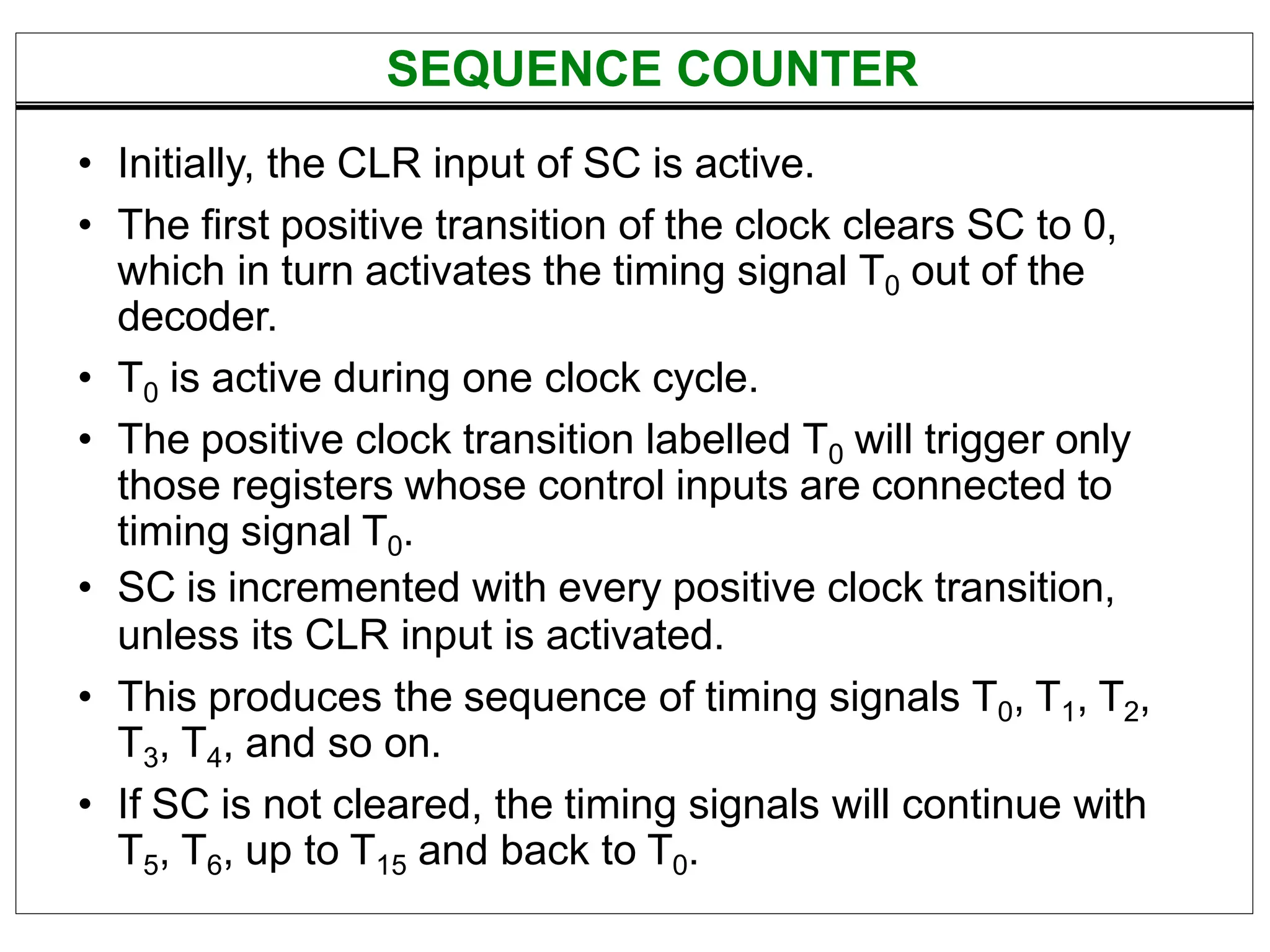
SEQUENCE COUNTER
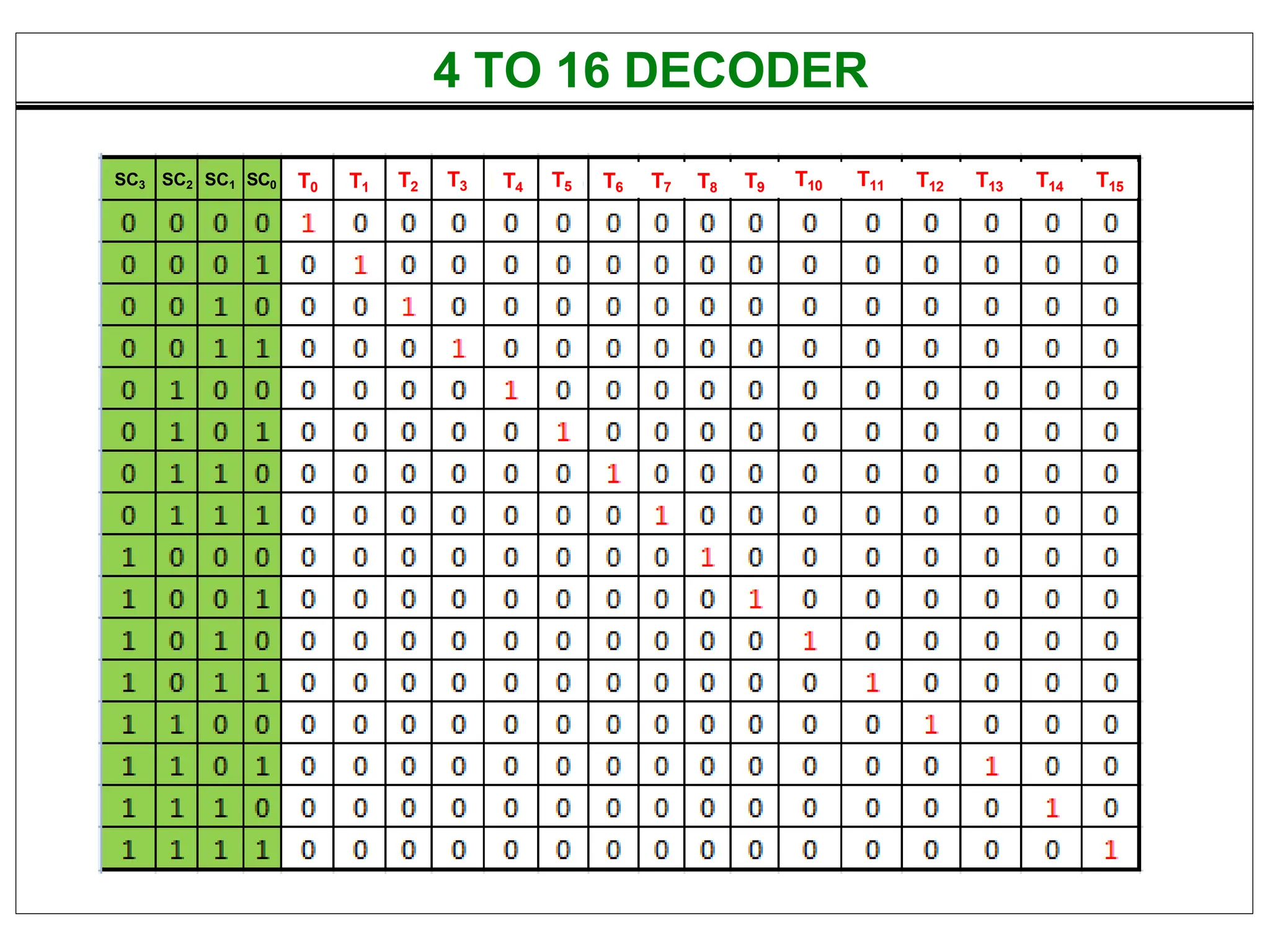
13.
• Initially, theCLR input of SC is active.
• The first positive transition of the clock clears SC to 0,
which in turn activates the timing signal T0 out of the
decoder.
• T0 is active during one clock cycle.
• The positive clock transition labelled T0 will trigger only
those registers whose control inputs are connected to
timing signal T0.
• SC is incremented with every positive clock transition,
unless its CLR input is activated.
• This produces the sequence of timing signals T0, T1, T2,
T3, T4, and so on.
• If SC is not cleared, the timing signals will continue with
T5, T6, up to T15 and back to T0.
SEQUENCE COUNTER
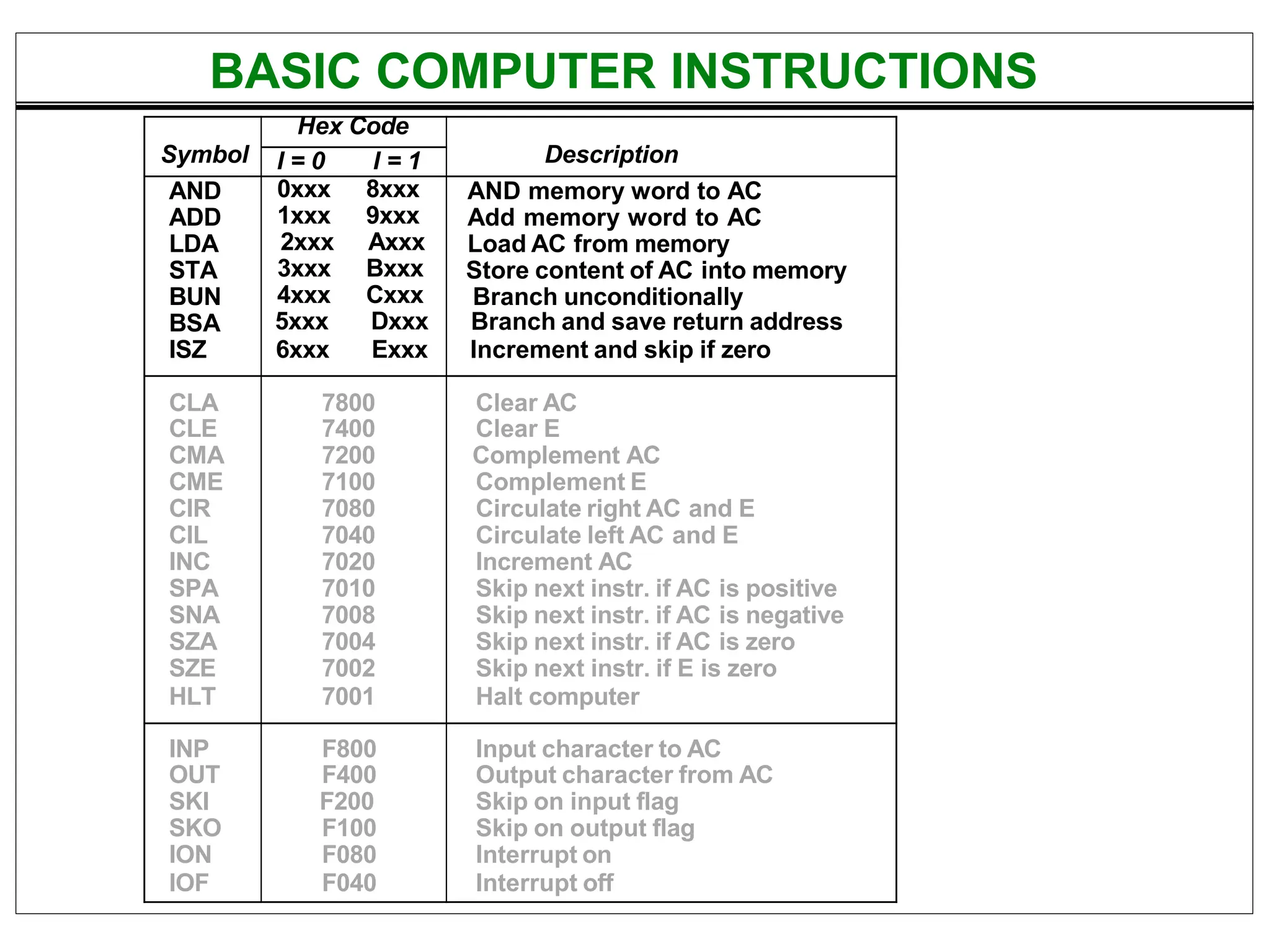
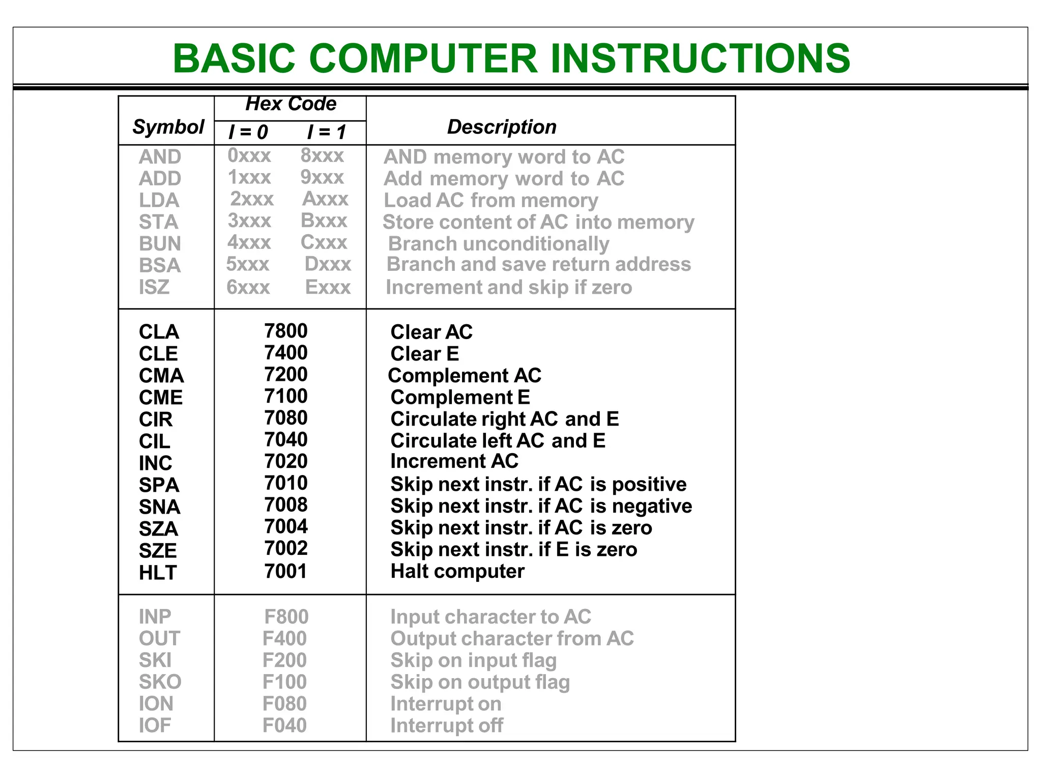
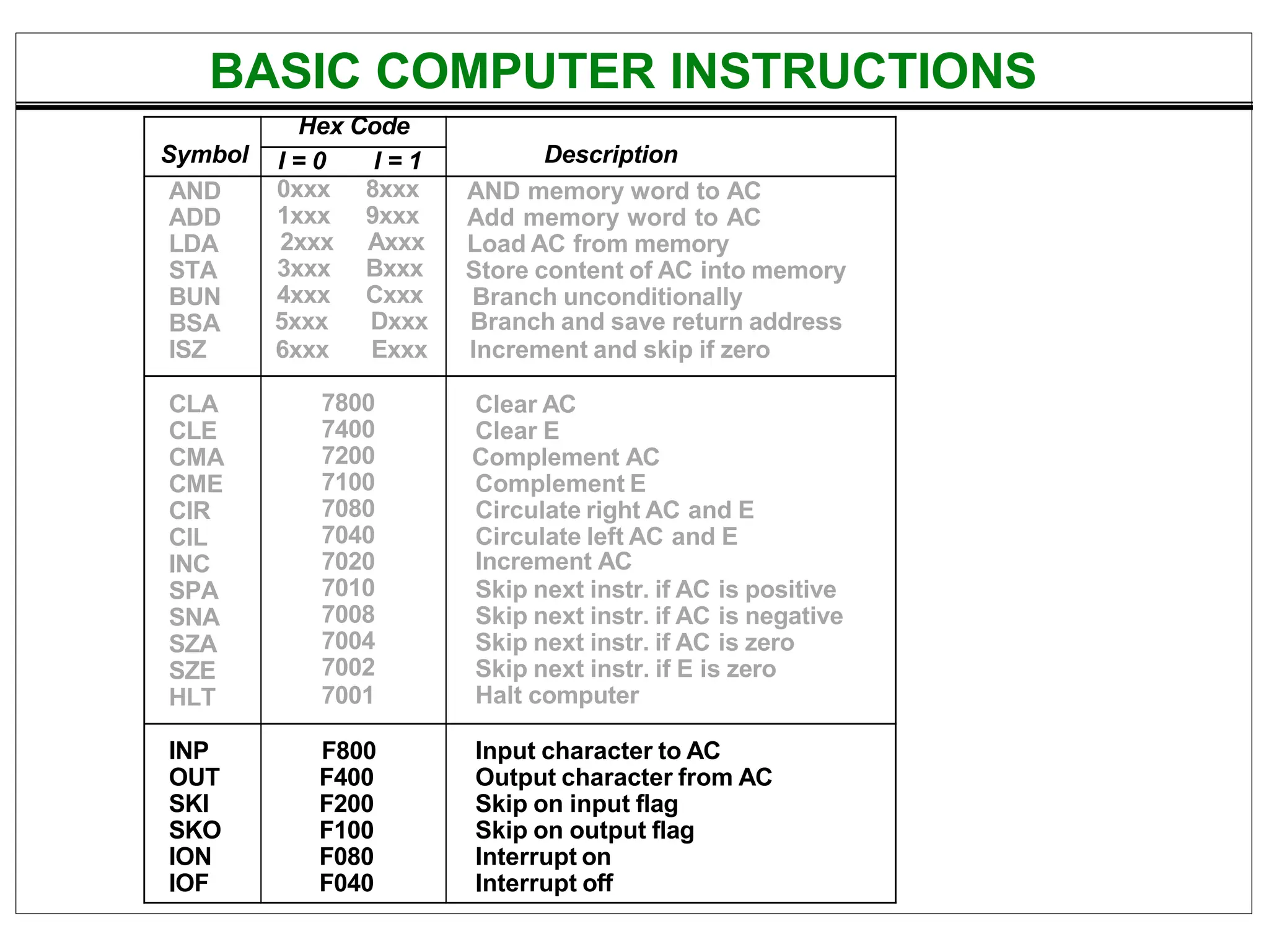
Symbol
Hex Code
Description
I =0 I = 1
AND
ADD
LDA
STA
BUN
BSA
ISZ
0xxx 8xxx
1xxx 9xxx
2xxx Axxx
3xxx Bxxx
4xxx Cxxx
5xxx Dxxx
6xxx Exxx
AND memory word to AC
Add memory word to AC
Load AC from memory
Store content of AC into memory
Branch unconditionally
Branch and save return address
Increment and skip if zero
CLA 7800 Clear AC
CLE 7400 Clear E
CMA 7200 Complement AC
CME 7100 Complement E
CIR 7080 Circulate right AC and E
CIL 7040 Circulate left AC and E
INC 7020 Increment AC
SPA 7010 Skip next instr. if AC is positive
SNA 7008 Skip next instr. if AC is negative
SZA 7004 Skip next instr. if AC is zero
SZE 7002 Skip next instr. if E is zero
HLT 7001 Halt computer
INP F800 Input character to AC
OUT F400 Output character from AC
SKI F200 Skip on input flag
SKO F100 Skip on output flag
ION F080 Interrupt on
IOF F040 Interrupt off
BASIC COMPUTER INSTRUCTIONS
17.
MEMORY-REFERENCE INSTRUCTIONS
The executionof memory-reference instructions starts at T4.
AND: AND to AC
D0T4:
D0T5:
DR M[AR]
AC AC DR, SC 0
ADD: ADD to AC
D1T4:
D1T5:
DR M[AR]
AC AC + DR, E Cout, SC 0
LDA: Load from Memory to AC
D2T4: DR M[AR]
D2T5: AC DR, SC 0
STA: Store AC in Memory
D3T4: M[AR] AC, SC 0
18.
20
PC = 21
0BSA 135
Next instruction
Subroutine
1 BUN 135
Memory
BUN: Branch Unconditionally
D4T4: PC AR, SC 0
BSA: Branch and Save Return Address
D5T4: M[AR] PC, AR AR + 1
D5T5: PC AR, SC 0
MEMORY-REFERENCE INSTRUCTIONS
Memory, PC, AR at T4
AR = 135
136
20
21
0 BSA 135
Next instruction
21
Subroutine
1 BUN 135
Memory
Memory, PC after execution
135
PC = 136
19.
ISZ: Increment andSkip-if-Zero
D6T4: DR M[AR]
D6T5: DR DR + 1
D6T6: M[AR] DR, if (DR = 0) then (PC PC + 1), SC 0
MEMORY-REFERENCE INSTRUCTIONS
20.
D7' I T3:
D7'I' T3:
D7 I' T3:
D7 I T3:
AR M[AR]
Nothing
Execute a Register-reference instruction
Execute an Input/Output instruction
Start
SC 0
= 0 (direct)
AR PC
T0
IR M[AR], PC PC + 1
T1
Decode op-code in IR(12-14),
AR IR(0-11), I IR(15)
T2
D7
= 0 (Memory-reference)
(Register or I/O) = 1
I
I
Execute
register-reference
instruction
SC 0
Execute
input/output
instruction
SC 0
AR M[AR] Nothing
= 0 (Register)
(I/O) = 1 (indirect) = 1
T3
Execute
memory-reference
instruction
SC 0
T4
T3 T3
T3
FLOWCHART FOR MEMORY-REFERENCE INSTRUCTIONS
21.
Execute memory-reference instruction
DR M[AR] DR M[AR] DR M[AR]
M[AR] AC
SC 0
AND ADD LDA STA
AC AC + DR
E Cout
SC 0
AC DR
SC 0
D0T4 D1T4 D2T4 D3T4
D0T5 D1T5 D2T5
PC AR
SC 0
M[AR] PC
AR AR + 1
DR M[AR]
BUN BSA ISZ
D4T4 D5T4 D6T4
DR DR + 1
D5T5 D6T5
PC AR
SC 0
M[AR] DR
if (DR = 0) then (PC PC + 1)
SC 0
D6T6
AC AC DR
SC 0
FLOWCHART FOR MEMORY-REFERENCE INSTRUCTIONS
Symbol
Hex Code
Description
I =0 I = 1
AND
ADD
LDA
STA
BUN
BSA
ISZ
0xxx 8xxx
1xxx 9xxx
2xxx Axxx
3xxx Bxxx
4xxx Cxxx
5xxx Dxxx
6xxx Exxx
AND memory word to AC
Add memory word to AC
Load AC from memory
Store content of AC into memory
Branch unconditionally
Branch and save return address
Increment and skip if zero
CLA
CLE
CMA
CME
CIR
CIL
INC
SPA
SNA
SZA
SZE
HLT
7800
7400
7200
7100
7080
7040
7020
7010
7008
7004
7002
7001
Clear AC
Clear E
Complement AC
Complement E
Circulate right AC and E
Circulate left AC and E
Increment AC
Skip next instr. if AC is positive
Skip next instr. if AC is negative
Skip next instr. if AC is zero
Skip next instr. if E is zero
Halt computer
INP
OUT
SKI
SKO
ION
IOF
F800
F400
F200
F100
F080
F040
Input character to AC
Output character from AC
Skip on input flag
Skip on output flag
Interrupt on
Interrupt off
BASIC COMPUTER INSTRUCTIONS
25.
DETERMINE THE TYPEOF INSTRUCTION
D7' I T3:
D7' I' T3:
D7 I' T3:
D7 I T3:
AR M[AR]
Nothing
Execute a Register-reference instruction
Execute an Input/Output instruction
Start
SC 0
= 0 (direct)
AR PC
T0
IR M[AR], PC PC + 1
T1
Decode op-code in IR(12-14),
AR IR(0-11), I IR(15)
T2
D7
= 0 (Memory-reference)
(Register or I/O) = 1
I
I
Execute
register-reference
instruction
SC 0
Execute
input/output
instruction
SC 0
AR M[AR] Nothing
= 0 (Register)
(I/O) = 1 (indirect) = 1
T3
Execute
memory-reference
instruction
SC 0
T4
T3 T3
T3
26.
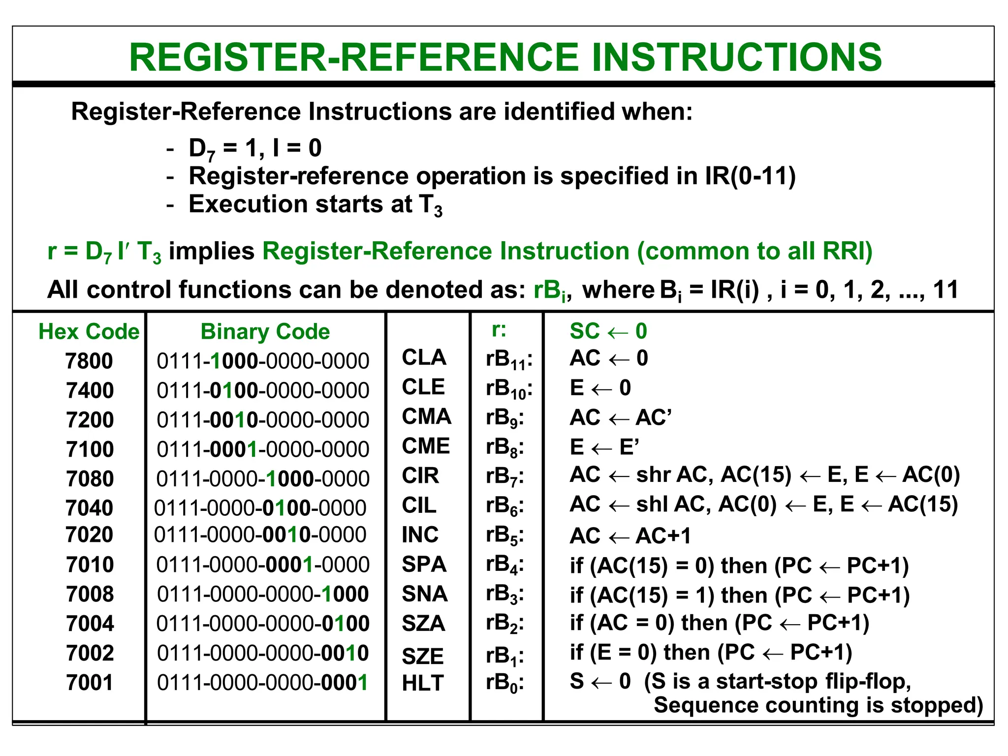
REGISTER-REFERENCE INSTRUCTIONS
Register-Reference Instructionsare identified when:
- D7 = 1, I = 0
- Register-reference operation is specified in IR(0-11)
- Execution starts at T3
r = D7 I T3 implies Register-Reference Instruction (common to all RRI)
All control functions can be denoted as: rBi, where Bi = IR(i) , i = 0, 1, 2, ..., 11
Hex Code Binary Code
CLA
CLE
CMA
CME
CIR
CIL
INC
SPA
SNA
SZA
SZE
HLT
r:
rB11:
rB10:
rB9:
rB8:
rB7:
rB6:
rB5:
rB4:
rB3:
rB2:
rB1:
rB0:
SC 0
AC 0
E 0
AC AC’
E E’
AC shr AC, AC(15) E, E AC(0)
AC shl AC, AC(0) E, E AC(15)
AC AC+1
if (AC(15) = 0) then (PC PC+1)
if (AC(15) = 1) then (PC PC+1)
if (AC = 0) then (PC PC+1)
if (E = 0) then (PC PC+1)
S 0 (S is a start-stop flip-flop,
Sequence counting is stopped)
7800 0111-1000-0000-0000
7400 0111-0100-0000-0000
7200 0111-0010-0000-0000
7100 0111-0001-0000-0000
7080 0111-0000-1000-0000
7040
7020
0111-0000-0100-0000
0111-0000-0010-0000
7010 0111-0000-0001-0000
7008 0111-0000-0000-1000
7004 0111-0000-0000-0100
7002 0111-0000-0000-0010
7001 0111-0000-0000-0001
Symbol
Hex Code
Description
I =0 I = 1
AND
ADD
LDA
STA
BUN
BSA
ISZ
0xxx 8xxx
1xxx 9xxx
2xxx Axxx
3xxx Bxxx
4xxx Cxxx
5xxx Dxxx
6xxx Exxx
AND memory word to AC
Add memory word to AC
Load AC from memory
Store content of AC into memory
Branch unconditionally
Branch and save return address
Increment and skip if zero
CLA
CLE
CMA
CME
CIR
CIL
INC
SPA
SNA
SZA
SZE
HLT
7800
7400
7200
7100
7080
7040
7020
7010
7008
7004
7002
7001
Clear AC
Clear E
Complement AC
Complement E
Circulate right AC and E
Circulate left AC and E
Increment AC
Skip next instr. if AC is positive
Skip next instr. if AC is negative
Skip next instr. if AC is zero
Skip next instr. if E is zero
Halt computer
INP
OUT
SKI
SKO
ION
IOF
F800
F400
F200
F100
F080
F040
Input character to AC
Output character from AC
Skip on input flag
Skip on output flag
Interrupt on
Interrupt off
BASIC COMPUTER INSTRUCTIONS
30.
DETERMINE THE TYPEOF INSTRUCTION
D7' I T3:
D7' I' T3:
D7 I' T3:
D7 I T3:
AR M[AR]
Nothing
Execute a Register-reference instruction
Execute an Input/Output instruction
Start
SC 0
= 0 (direct)
AR PC
T0
IR M[AR], PC PC + 1
T1
Decode op-code in IR(12-14),
AR IR(0-11), I IR(15)
T2
D7
= 0 (Memory-reference)
(Register or I/O) = 1
I
I
Execute
register-reference
instruction
SC 0
Execute
input/output
instruction
SC 0
AR M[AR] Nothing
= 0 (Register)
(I/O) = 1 (indirect) = 1
T3
Execute
memory-reference
instruction
SC 0
T4
T3 T3
T3
31.
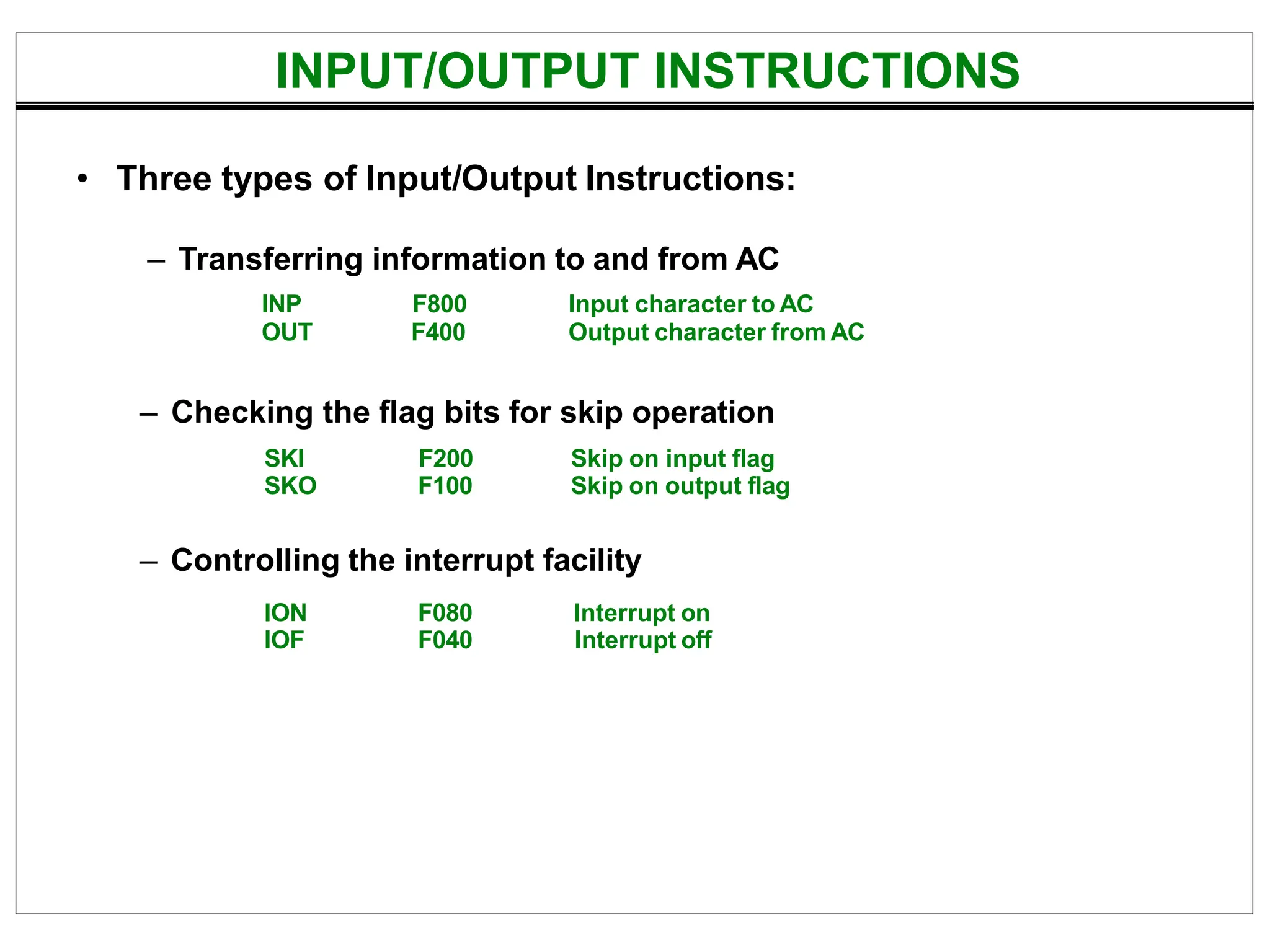
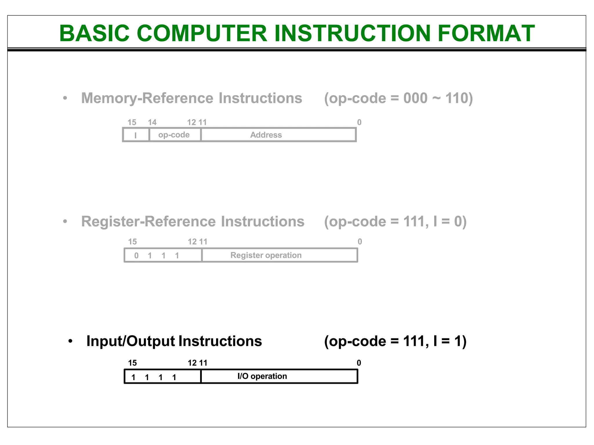
INPUT/OUTPUT INSTRUCTIONS
• Threetypes of Input/Output Instructions:
– Checking the flag bits for skip operation
– Controlling the interrupt facility
INP
OUT
F800
F400
Input character to AC
Output character from AC
SKI F200 Skip on input flag
SKO F100 Skip on output flag
ION F080 Interrupt on
IOF F040 Interrupt off
– Transferring information to and from AC
32.
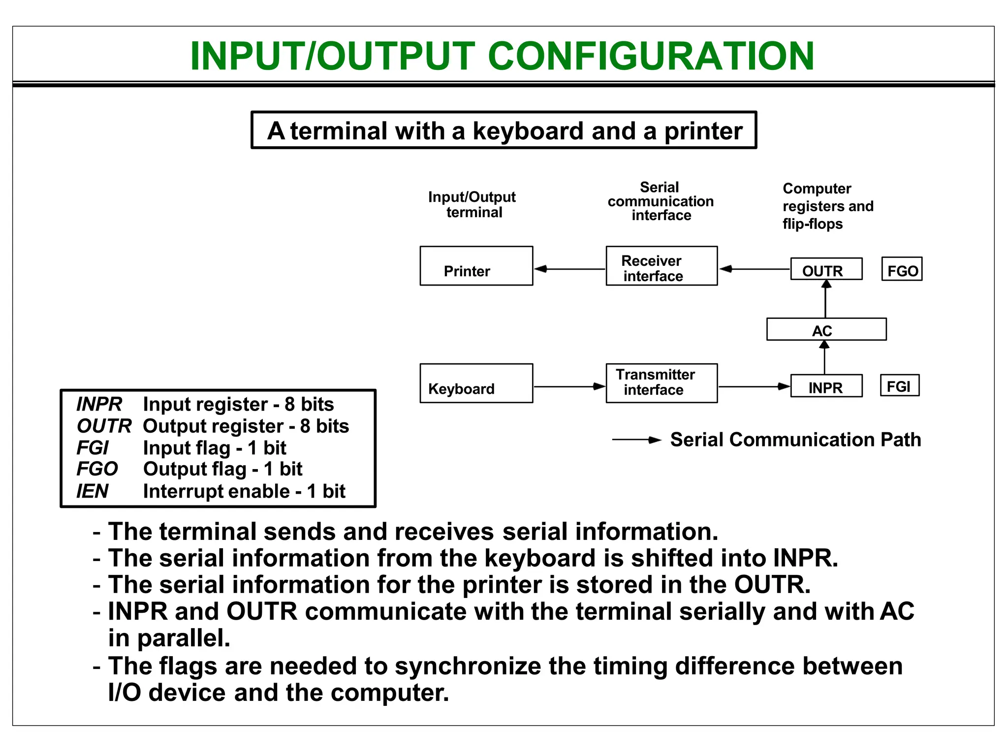
INPUT/OUTPUT CONFIGURATION
INPR Inputregister - 8 bits
OUTR Output register - 8 bits
FGI Input flag - 1 bit
FGO Output flag - 1 bit
IEN Interrupt enable - 1 bit
- The terminal sends and receives serial information.
- The serial information from the keyboard is shifted into INPR.
- The serial information for the printer is stored in the OUTR.
- INPR and OUTR communicate with the terminal serially and with AC
in parallel.
- The flags are needed to synchronize the timing difference between
I/O device and the computer.
A terminal with a keyboard and a printer
Input/Output
terminal
Serial
communication
interface
Computer
registers and
flip-flops
Printer
Keyboard
Receiver
interface
Transmitter
interface
FGO
OUTR
AC
INPR FGI
Serial Communication Path
33.
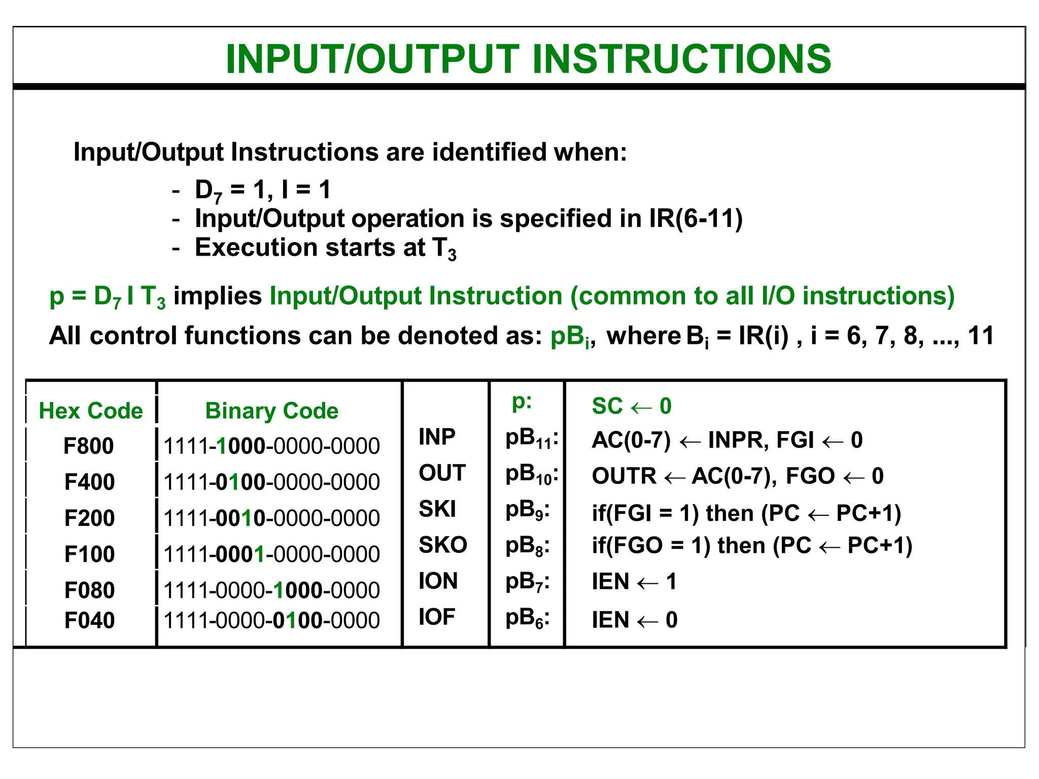
INPUT/OUTPUT INSTRUCTIONS
Input/Output Instructionsare identified when:
- D7 = 1, I = 1
- Input/Output operation is specified in IR(6-11)
- Execution starts at T3
p = D7 I T3 implies Input/Output Instruction (common to all I/O instructions)
All control functions can be denoted as: pBi, where Bi = IR(i) , i = 6, 7, 8, ..., 11
INP
OUT
SKI
SKO
ION
IOF
p:
pB11:
pB10:
pB9:
pB8:
pB7:
pB6:
SC 0
AC(0-7) INPR, FGI 0
OUTR AC(0-7), FGO 0
if(FGI = 1) then (PC PC+1)
if(FGO = 1) then (PC PC+1)
IEN 1
IEN 0
Hex Code Binary Code
F800 1111-1000-0000-0000
F400 1111-0100-0000-0000
F200 1111-0010-0000-0000
F100 1111-0001-0000-0000
F080 1111-0000-1000-0000
F040 1111-0000-0100-0000
34.
PROGRAM CONTROLLED DATATRANSFER
FGO=0
END
yes
yes More
Character
no
OUTR AC(0-7)
FGO 0
no
FGO=0
FGO = 1: Output device is available/not busy
_________
END
yes
no
More
Character
AC(0-7) INPR
FGI 0
FGI=0
no
FGI=0
FGI = 1: Information in INPR cannot be changed by
pressing another key
yes
![FETCH and DECODE
Fetch and Decode
T0: AR PC (S2S1S0 = 010, T0 = 1)
T1: IR M[AR], PC PC + 1 (S2S1S0 = 111, T1 = 1)
T2: D0, . . . , D7 Decode IR(12-14),AR IR(0-11), I IR(15)
S2
S1
S0
Bus
7
Memory
unit
AR
LD
PC
INR
IR
LD
Clock
1
2
5
Common bus
T1
T0
Address
Read](https://image.slidesharecdn.com/ce222slides5-250322081457-86d1e987/75/computer-organization-and-assembly-language-giki-course-slides-4-2048.jpg)
![DETERMINE THE TYPE OF INSTRUCTION
D7' I T3:
D7' I' T3:
D7 I' T3:
D7 I T3:
AR M[AR]
Nothing
Execute a Register-reference instruction
Execute an Input/Output instruction
Start
SC 0
= 0 (direct)
AR PC
T0
IR M[AR], PC PC + 1
T1
Decode op-code in IR(12-14),
AR IR(0-11), I IR(15)
T2
D7
= 0 (Memory-reference)
(Register or I/O) = 1
I
I
Execute
register-reference
instruction
SC 0
Execute
input/output
instruction
SC 0
AR M[AR] Nothing
= 0 (Register)
(I/O) = 1 (indirect) = 1
T3
Execute
memory-reference
instruction
SC 0
T4
T3 T3
T3](https://image.slidesharecdn.com/ce222slides5-250322081457-86d1e987/75/computer-organization-and-assembly-language-giki-course-slides-7-2048.jpg)
![MEMORY-REFERENCE INSTRUCTIONS
The execution of memory-reference instructions starts at T4.
AND: AND to AC
D0T4:
D0T5:
DR M[AR]
AC AC DR, SC 0
ADD: ADD to AC
D1T4:
D1T5:
DR M[AR]
AC AC + DR, E Cout, SC 0
LDA: Load from Memory to AC
D2T4: DR M[AR]
D2T5: AC DR, SC 0
STA: Store AC in Memory
D3T4: M[AR] AC, SC 0](https://image.slidesharecdn.com/ce222slides5-250322081457-86d1e987/75/computer-organization-and-assembly-language-giki-course-slides-17-2048.jpg)
![20
PC = 21
0 BSA 135
Next instruction
Subroutine
1 BUN 135
Memory
BUN: Branch Unconditionally
D4T4: PC AR, SC 0
BSA: Branch and Save Return Address
D5T4: M[AR] PC, AR AR + 1
D5T5: PC AR, SC 0
MEMORY-REFERENCE INSTRUCTIONS
Memory, PC, AR at T4
AR = 135
136
20
21
0 BSA 135
Next instruction
21
Subroutine
1 BUN 135
Memory
Memory, PC after execution
135
PC = 136](https://image.slidesharecdn.com/ce222slides5-250322081457-86d1e987/75/computer-organization-and-assembly-language-giki-course-slides-18-2048.jpg)
![ISZ: Increment and Skip-if-Zero
D6T4: DR M[AR]
D6T5: DR DR + 1
D6T6: M[AR] DR, if (DR = 0) then (PC PC + 1), SC 0
MEMORY-REFERENCE INSTRUCTIONS](https://image.slidesharecdn.com/ce222slides5-250322081457-86d1e987/75/computer-organization-and-assembly-language-giki-course-slides-19-2048.jpg)
![D7' I T3:
D7' I' T3:
D7 I' T3:
D7 I T3:
AR M[AR]
Nothing
Execute a Register-reference instruction
Execute an Input/Output instruction
Start
SC 0
= 0 (direct)
AR PC
T0
IR M[AR], PC PC + 1
T1
Decode op-code in IR(12-14),
AR IR(0-11), I IR(15)
T2
D7
= 0 (Memory-reference)
(Register or I/O) = 1
I
I
Execute
register-reference
instruction
SC 0
Execute
input/output
instruction
SC 0
AR M[AR] Nothing
= 0 (Register)
(I/O) = 1 (indirect) = 1
T3
Execute
memory-reference
instruction
SC 0
T4
T3 T3
T3
FLOWCHART FOR MEMORY-REFERENCE INSTRUCTIONS](https://image.slidesharecdn.com/ce222slides5-250322081457-86d1e987/75/computer-organization-and-assembly-language-giki-course-slides-20-2048.jpg)
![Execute memory-reference instruction
DR M[AR] DR M[AR] DR M[AR]
M[AR] AC
SC 0
AND ADD LDA STA
AC AC + DR
E Cout
SC 0
AC DR
SC 0
D0T4 D1T4 D2T4 D3T4
D0T5 D1T5 D2T5
PC AR
SC 0
M[AR] PC
AR AR + 1
DR M[AR]
BUN BSA ISZ
D4T4 D5T4 D6T4
DR DR + 1
D5T5 D6T5
PC AR
SC 0
M[AR] DR
if (DR = 0) then (PC PC + 1)
SC 0
D6T6
AC AC DR
SC 0
FLOWCHART FOR MEMORY-REFERENCE INSTRUCTIONS](https://image.slidesharecdn.com/ce222slides5-250322081457-86d1e987/75/computer-organization-and-assembly-language-giki-course-slides-21-2048.jpg)
![DETERMINE THE TYPE OF INSTRUCTION
D7' I T3:
D7' I' T3:
D7 I' T3:
D7 I T3:
AR M[AR]
Nothing
Execute a Register-reference instruction
Execute an Input/Output instruction
Start
SC 0
= 0 (direct)
AR PC
T0
IR M[AR], PC PC + 1
T1
Decode op-code in IR(12-14),
AR IR(0-11), I IR(15)
T2
D7
= 0 (Memory-reference)
(Register or I/O) = 1
I
I
Execute
register-reference
instruction
SC 0
Execute
input/output
instruction
SC 0
AR M[AR] Nothing
= 0 (Register)
(I/O) = 1 (indirect) = 1
T3
Execute
memory-reference
instruction
SC 0
T4
T3 T3
T3](https://image.slidesharecdn.com/ce222slides5-250322081457-86d1e987/75/computer-organization-and-assembly-language-giki-course-slides-25-2048.jpg)
![DETERMINE THE TYPE OF INSTRUCTION
D7' I T3:
D7' I' T3:
D7 I' T3:
D7 I T3:
AR M[AR]
Nothing
Execute a Register-reference instruction
Execute an Input/Output instruction
Start
SC 0
= 0 (direct)
AR PC
T0
IR M[AR], PC PC + 1
T1
Decode op-code in IR(12-14),
AR IR(0-11), I IR(15)
T2
D7
= 0 (Memory-reference)
(Register or I/O) = 1
I
I
Execute
register-reference
instruction
SC 0
Execute
input/output
instruction
SC 0
AR M[AR] Nothing
= 0 (Register)
(I/O) = 1 (indirect) = 1
T3
Execute
memory-reference
instruction
SC 0
T4
T3 T3
T3](https://image.slidesharecdn.com/ce222slides5-250322081457-86d1e987/75/computer-organization-and-assembly-language-giki-course-slides-30-2048.jpg)