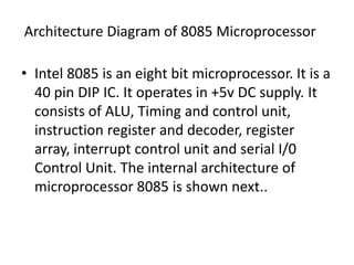
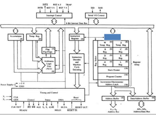
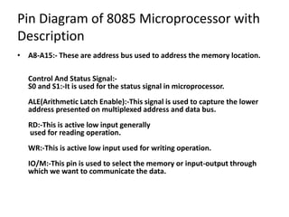
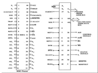
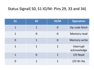
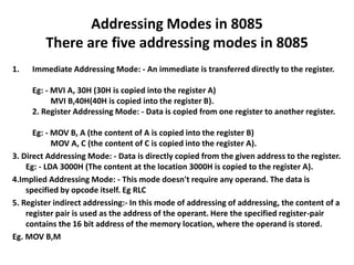
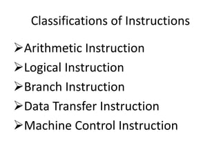
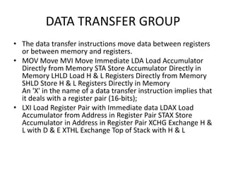
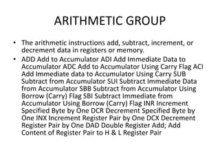
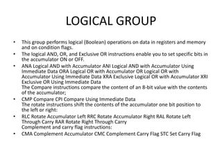
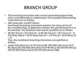
Excel Polytechnic College
Dept: Electronics and communication Engineering
Subject: Digital Electronics
Unit: Microprocessor-8085
Introduction to Microprocessor
8085 Microprocessor Definition:
It is a single integrated circuit
• As we know that all of this operation is
performed Generally all of this operation is
done by the ALU unit in Microprocessor.
• by the CPU in a large computer.
• So we can compare the CPU and ALU as the
fig. given below.
• Microprocessor is a single chip integrated circuit.
It is a digital device working with binary numbers
“0” and “1”. It contain arithmetic logic unit(ALU),
control circuitry and the small amount of
memory.
• The microprocessor works under the control of a
program. It can fetch instructions from memory,
decode and execute them. Microprocessor is
fabricated by using VLSI Technology.
• Microprocessor has the ability to control of
input/output devices and to transfer information
to and from the memory. It acts as central
processing unit(CPU) of micro computer system.
Microprocessor with memory, input and output
devices is called a microcomputer.
Evolution of Microprocessors
• The first microprocessor Intel 4004 introduced in 1971.
• The other 4-bit microprocessor were Intel’s 4040, Toshiba’s
T3472, Rockwell’s PPS4, etc..
• In 1973 Intel introduced its first 8-bit microprocessor of 8008.
• At present here number of ,microprocessors in 8-bit namely
Intel 8085, Motorola’s M6800, M6809, Zilog,s Z80 and Z800.
• Followed this the first 12-bit and 16-bit microprocessors from
Intersils’s IM6100 and Toshiba’s T3190
• Examples of 16-bits namely Intel’s 8086, 80186 and 80286,
Motorola’s MC68000, Zilog’s Z8000 SERIES, Texes instruments
TMS 99000, Fairchild 9440 and digital equipments LSI II
DEFINITIONS OF TERM USED IN MICROPROCESSOR
Central Processing unit (CPU)
It works as the heart of the computer. It contains
Arithmetic-logic unit, some registers and control circuits.
Arithmetic and logic unit (ALU)
It performs arithmetic operations such as addition,
subtraction, etc.. And logic operations like AND, OR, EX-OR
etc,..
Control unit
It produces necessary timing and control signals for
doing all functions in computer
Bit
Bit is Binary Digit ‘0’ and ’1’
Bytes
Bytes is combination of ‘8’ bits.
Nibble
Nibble is a group of ‘4’ bits
Word
Word is a group of bits, the computer recognizers and the
processor at a time.
Instruction
Instruction is a command, recognized and executed by a
microprocessor.
Program
Program is set of instructions written for the computer to
perform a tusk.
Bus
Bus is a group of lines, used to transfer information (binary
bits 0 and 1). There are three types of buses,.. Namely
Address Bus, Data Bus and control bus.
Peripherals
I/O devices connected to microprocessor are known as peripherals.
Sometimes memory may be treated as peripherals.
Mnemonics
Mnemonic is a combination of alphabet, understand the operation by
the users.
Compiler
Compiler is a program used for converting high level language into
machine language.
Assembler
It is a program used for converting assembly language to machine
language.
Software
Software is a Combination of program.
Hardware
The Physical components placed in the computer are called hardware.
Firmware
The software stored in ROM, PROM and EPROM is
called Firmware.
Buffer
Buffer is a logic circuit used for increase current
and power amount.
Tri-state buffer
buffer with control terminal is called Tristate
buffer. It contain three types of outputs, namely;
low, high and high impedence.
Latch
Latch is a temporary memory unit. It is used for
controlling the signal flow.
Arithmetic And Logic Unit
• This section is used for performing the
arithmetic and logical operation in
Microprocessor. Here A and B are the input pins
where operands are put on which we want to
perform arithmetic and logical operation. A and
B section are operand section and it processes it
according to the given instruction.
• Arithmetic operation:- Like addition,
subtraction, multiplication, division etc.
Block Diagram Of ALU
Architecture Diagram of 8085 Microprocessor
• Intel 8085 is an eight bit microprocessor. It is a
40 pin DIP IC. It operates in +5v DC supply. It
consists of ALU, Timing and control unit,
instruction register and decoder, register
array, interrupt control unit and serial I/0
Control Unit. The internal architecture of
microprocessor 8085 is shown next..
Pin Diagram of 8085 Microprocessor with
Description
• A8-A15:- These are address bus used to address the memory location.
Control And Status Signal:-
S0 and S1:-It is used for the status signal in microprocessor.
ALE(Arithmetic Latch Enable):-This signal is used to capture the lower
address presented on multiplexed address and data bus.
RD:-This is active low input generally
used for reading operation.
WR:-This is active low input used for writing operation.
IO/M:-This pin is used to select the memory or input-output through
which we want to communicate the data.
Status Signal( S0, S1 IO/M- Pins 29, 33 and 34)
S1 S0 IO/M Operation
1 1 0 Op code fetch
1 0 0 Memory read
0 1 0 Memory write
1 1 1 Interrupt
acknowledge
1 0 1 I/O Read
0 1 1 I/O W rite
Addressing Modes in 8085
There are five addressing modes in 8085
1. Immediate Addressing Mode: - An immediate is transferred directly to the register.
Eg: - MVI A, 30H (30H is copied into the register A)
MVI B,40H(40H is copied into the register B).
2. Register Addressing Mode: - Data is copied from one register to another register.
Eg: - MOV B, A (the content of A is copied into the register B)
MOV A, C (the content of C is copied into the register A).
3. Direct Addressing Mode: - Data is directly copied from the given address to the register.
Eg: - LDA 3000H (The content at the location 3000H is copied to the register A).
4.Implied Addressing Mode: - This mode doesn't require any operand. The data is
specified by opcode itself. Eg RLC
5. Register indirect addressing:- In this mode of addressing of addressing, the content of a
register pair is used as the address of the operant. Here the specified register-pair
contains the 16 bit address of the memory location, where the operand is stored.
Eg. MOV B,M
Classifications of Instructions
Arithmetic Instruction
Logical Instruction
Branch Instruction
Data Transfer Instruction
Machine Control Instruction
DATA TRANSFER GROUP
• The data transfer instructions move data between registers
or between memory and registers.
• MOV Move MVI Move Immediate LDA Load Accumulator
Directly from Memory STA Store Accumulator Directly in
Memory LHLD Load H & L Registers Directly from Memory
SHLD Store H & L Registers Directly in Memory
An 'X' in the name of a data transfer instruction implies that
it deals with a register pair (16-bits);
• LXI Load Register Pair with Immediate data LDAX Load
Accumulator from Address in Register Pair STAX Store
Accumulator in Address in Register Pair XCHG Exchange H &
L with D & E XTHL Exchange Top of Stack with H & L
ARITHMETIC GROUP
• The arithmetic instructions add, subtract, increment, or
decrement data in registers or memory.
• ADD Add to Accumulator ADI Add Immediate Data to
Accumulator ADC Add to Accumulator Using Carry Flag ACI
Add Immediate data to Accumulator Using Carry SUB
Subtract from Accumulator SUI Subtract Immediate Data
from Accumulator SBB Subtract from Accumulator Using
Borrow (Carry) Flag SBI Subtract Immediate from
Accumulator Using Borrow (Carry) Flag INR Increment
Specified Byte by One DCR Decrement Specified Byte by
One INX Increment Register Pair by One DCX Decrement
Register Pair by One DAD Double Register Add; Add
Content of Register Pair to H & L Register Pair
LOGICAL GROUP
• This group performs logical (Boolean) operations on data in registers and memory
and on condition flags.
• The logical AND, OR, and Exclusive OR instructions enable you to set specific bits in
the accumulator ON or OFF.
• ANA Logical AND with Accumulator ANI Logical AND with Accumulator Using
Immediate Data ORA Logical OR with Accumulator OR Logical OR with
Accumulator Using Immediate Data XRA Exclusive Logical OR with Accumulator XRI
Exclusive OR Using Immediate Data
The Compare instructions compare the content of an 8-bit value with the contents
of the accumulator;
• CMP Compare CPI Compare Using Immediate Data
The rotate instructions shift the contents of the accumulator one bit position to
the left or right:
• RLC Rotate Accumulator Left RRC Rotate Accumulator Right RAL Rotate Left
Through Carry RAR Rotate Right Through Carry
Complement and carry flag instructions:
• CMA Complement Accumulator CMC Complement Carry Flag STC Set Carry Flag
BRANCH GROUP
• The branching instructions alter normal sequential program flow,
either unconditionally or conditionally. The unconditional branching
instructions are as follows:
• JMP Jump CALL Call RET Return
Conditional branching instructions examine the status of one of
four condition flags to determine whether the specified branch is to
be executed. The conditions that may be specified are as follows:
• NZ Not Zero (Z = 0) Z Zero (Z = 1) NC No Carry (C = 0) C Carry (C = 1)
PO Parity Odd (P = 0) PE Parity Even (P = 1) P Plus (S = 0) M Minus (S
= 1)
Thus, the conditional branching instructions are specified as
follows:
• Jumps Calls Returns C CC RC (Carry) INC CNC RNC (No Carry) JZ CZ
RZ (Zero) JNZ CNZ RNZ (Not Zero) JP CP RP (Plus) JM CM RM (Minus)
JPE CPE RPE (Parity Even) JP0 CPO RPO (Parity Odd)
Stack I-O and Machine Control
Instructions
• The following instructions affect the Stack and/or Stack
Pointer:
• PUSH-Push Two bytes of Data onto the Stack POP Pop
Two Bytes of Data off the Stack XTHL Exchange Top of
Stack with H & L SPHL Move content of H & L to Stack
Pointer
The I/0 instructions are as follows:
• IN-Initiate Input Operation OUT Initiate Output
Operation
The Machine Control instructions are as follows:
• EI-Enable Interrupt System DI Disable Interrupt System
HLT Halt NOP No Operation
Memory-mapped I/O
• Memory-mapped I/O (MMIO) and port-mapped I/O (PMIO) (which is also
called isolated I/O) are two complementary methods of
performing input/output (I/O) between the central processing unit (CPU)
and peripheral devices in a computer. An alternative approach is using dedicated
I/O processors, commonly known as channels on mainframe computers, which
execute their own instructions.
• Memory-mapped I/O uses the same address space to address
both memory and I/O devices. The memory and registers of the I/O devices are
mapped to (associated with) address values. So when an address is accessed by
the CPU, it may refer to a portion of physical RAM, or it can instead refer to
memory of the I/O device. Thus, the CPU instructions used to access the memory
can also be used for accessing devices. Each I/O device monitors the CPU's address
bus and responds to any CPU access of an address assigned to that device,
connecting the data bus to the desired device's hardware register. To
accommodate the I/O devices, areas of the addresses used by the CPU must be
reserved for I/O and must not be available for normal physical memory. The
reservation may be permanent, or temporary (as achieved via bank switching). An
example of the latter is found in the Commodore 64, which uses a form of memory
mapping to cause RAM or I/O hardware
Instruction Cycle
• An instruction cycle (sometimes called a fetch–decode–execute
cycle) is the basic operational process of a computer. It is the
process by which a computer retrieves a program instruction from
its memory, determines what actions the instruction dictates, and
carries out those actions. This cycle is repeated continuously by a
computer's central processing unit (CPU), from boot-up to when
the computer is shut down.
• In simpler CPUs the instruction cycle is executed sequentially, each
instruction being processed before the next one is started. In most
modern CPUs the instruction cycles are instead
executed concurrently, and often in parallel, through an instruction
pipeline: the next instruction starts being processed before the
previous instruction has finished, which is possible because the
cycle is broken up into separate steps.
8085 Timing Drawing

5th unit Microprocessor 8085

  • 1.
    Excel Polytechnic College Dept:Electronics and communication Engineering Subject: Digital Electronics Unit: Microprocessor-8085
  • 2.
    Introduction to Microprocessor 8085Microprocessor Definition: It is a single integrated circuit • As we know that all of this operation is performed Generally all of this operation is done by the ALU unit in Microprocessor. • by the CPU in a large computer. • So we can compare the CPU and ALU as the fig. given below.
  • 3.
    • Microprocessor isa single chip integrated circuit. It is a digital device working with binary numbers “0” and “1”. It contain arithmetic logic unit(ALU), control circuitry and the small amount of memory. • The microprocessor works under the control of a program. It can fetch instructions from memory, decode and execute them. Microprocessor is fabricated by using VLSI Technology. • Microprocessor has the ability to control of input/output devices and to transfer information to and from the memory. It acts as central processing unit(CPU) of micro computer system. Microprocessor with memory, input and output devices is called a microcomputer.
  • 4.
    Evolution of Microprocessors •The first microprocessor Intel 4004 introduced in 1971. • The other 4-bit microprocessor were Intel’s 4040, Toshiba’s T3472, Rockwell’s PPS4, etc.. • In 1973 Intel introduced its first 8-bit microprocessor of 8008. • At present here number of ,microprocessors in 8-bit namely Intel 8085, Motorola’s M6800, M6809, Zilog,s Z80 and Z800. • Followed this the first 12-bit and 16-bit microprocessors from Intersils’s IM6100 and Toshiba’s T3190 • Examples of 16-bits namely Intel’s 8086, 80186 and 80286, Motorola’s MC68000, Zilog’s Z8000 SERIES, Texes instruments TMS 99000, Fairchild 9440 and digital equipments LSI II
  • 5.
    DEFINITIONS OF TERMUSED IN MICROPROCESSOR Central Processing unit (CPU) It works as the heart of the computer. It contains Arithmetic-logic unit, some registers and control circuits. Arithmetic and logic unit (ALU) It performs arithmetic operations such as addition, subtraction, etc.. And logic operations like AND, OR, EX-OR etc,.. Control unit It produces necessary timing and control signals for doing all functions in computer Bit Bit is Binary Digit ‘0’ and ’1’
  • 6.
    Bytes Bytes is combinationof ‘8’ bits. Nibble Nibble is a group of ‘4’ bits Word Word is a group of bits, the computer recognizers and the processor at a time. Instruction Instruction is a command, recognized and executed by a microprocessor. Program Program is set of instructions written for the computer to perform a tusk. Bus Bus is a group of lines, used to transfer information (binary bits 0 and 1). There are three types of buses,.. Namely Address Bus, Data Bus and control bus.
  • 7.
    Peripherals I/O devices connectedto microprocessor are known as peripherals. Sometimes memory may be treated as peripherals. Mnemonics Mnemonic is a combination of alphabet, understand the operation by the users. Compiler Compiler is a program used for converting high level language into machine language. Assembler It is a program used for converting assembly language to machine language. Software Software is a Combination of program. Hardware The Physical components placed in the computer are called hardware.
  • 8.
    Firmware The software storedin ROM, PROM and EPROM is called Firmware. Buffer Buffer is a logic circuit used for increase current and power amount. Tri-state buffer buffer with control terminal is called Tristate buffer. It contain three types of outputs, namely; low, high and high impedence. Latch Latch is a temporary memory unit. It is used for controlling the signal flow.
  • 9.
    Arithmetic And LogicUnit • This section is used for performing the arithmetic and logical operation in Microprocessor. Here A and B are the input pins where operands are put on which we want to perform arithmetic and logical operation. A and B section are operand section and it processes it according to the given instruction. • Arithmetic operation:- Like addition, subtraction, multiplication, division etc.
  • 10.
  • 11.
    Architecture Diagram of8085 Microprocessor • Intel 8085 is an eight bit microprocessor. It is a 40 pin DIP IC. It operates in +5v DC supply. It consists of ALU, Timing and control unit, instruction register and decoder, register array, interrupt control unit and serial I/0 Control Unit. The internal architecture of microprocessor 8085 is shown next..
  • 13.
    Pin Diagram of8085 Microprocessor with Description • A8-A15:- These are address bus used to address the memory location. Control And Status Signal:- S0 and S1:-It is used for the status signal in microprocessor. ALE(Arithmetic Latch Enable):-This signal is used to capture the lower address presented on multiplexed address and data bus. RD:-This is active low input generally used for reading operation. WR:-This is active low input used for writing operation. IO/M:-This pin is used to select the memory or input-output through which we want to communicate the data.
  • 15.
    Status Signal( S0,S1 IO/M- Pins 29, 33 and 34) S1 S0 IO/M Operation 1 1 0 Op code fetch 1 0 0 Memory read 0 1 0 Memory write 1 1 1 Interrupt acknowledge 1 0 1 I/O Read 0 1 1 I/O W rite
  • 16.
    Addressing Modes in8085 There are five addressing modes in 8085 1. Immediate Addressing Mode: - An immediate is transferred directly to the register. Eg: - MVI A, 30H (30H is copied into the register A) MVI B,40H(40H is copied into the register B). 2. Register Addressing Mode: - Data is copied from one register to another register. Eg: - MOV B, A (the content of A is copied into the register B) MOV A, C (the content of C is copied into the register A). 3. Direct Addressing Mode: - Data is directly copied from the given address to the register. Eg: - LDA 3000H (The content at the location 3000H is copied to the register A). 4.Implied Addressing Mode: - This mode doesn't require any operand. The data is specified by opcode itself. Eg RLC 5. Register indirect addressing:- In this mode of addressing of addressing, the content of a register pair is used as the address of the operant. Here the specified register-pair contains the 16 bit address of the memory location, where the operand is stored. Eg. MOV B,M
  • 17.
    Classifications of Instructions ArithmeticInstruction Logical Instruction Branch Instruction Data Transfer Instruction Machine Control Instruction
  • 18.
    DATA TRANSFER GROUP •The data transfer instructions move data between registers or between memory and registers. • MOV Move MVI Move Immediate LDA Load Accumulator Directly from Memory STA Store Accumulator Directly in Memory LHLD Load H & L Registers Directly from Memory SHLD Store H & L Registers Directly in Memory An 'X' in the name of a data transfer instruction implies that it deals with a register pair (16-bits); • LXI Load Register Pair with Immediate data LDAX Load Accumulator from Address in Register Pair STAX Store Accumulator in Address in Register Pair XCHG Exchange H & L with D & E XTHL Exchange Top of Stack with H & L
  • 19.
    ARITHMETIC GROUP • Thearithmetic instructions add, subtract, increment, or decrement data in registers or memory. • ADD Add to Accumulator ADI Add Immediate Data to Accumulator ADC Add to Accumulator Using Carry Flag ACI Add Immediate data to Accumulator Using Carry SUB Subtract from Accumulator SUI Subtract Immediate Data from Accumulator SBB Subtract from Accumulator Using Borrow (Carry) Flag SBI Subtract Immediate from Accumulator Using Borrow (Carry) Flag INR Increment Specified Byte by One DCR Decrement Specified Byte by One INX Increment Register Pair by One DCX Decrement Register Pair by One DAD Double Register Add; Add Content of Register Pair to H & L Register Pair
  • 20.
    LOGICAL GROUP • Thisgroup performs logical (Boolean) operations on data in registers and memory and on condition flags. • The logical AND, OR, and Exclusive OR instructions enable you to set specific bits in the accumulator ON or OFF. • ANA Logical AND with Accumulator ANI Logical AND with Accumulator Using Immediate Data ORA Logical OR with Accumulator OR Logical OR with Accumulator Using Immediate Data XRA Exclusive Logical OR with Accumulator XRI Exclusive OR Using Immediate Data The Compare instructions compare the content of an 8-bit value with the contents of the accumulator; • CMP Compare CPI Compare Using Immediate Data The rotate instructions shift the contents of the accumulator one bit position to the left or right: • RLC Rotate Accumulator Left RRC Rotate Accumulator Right RAL Rotate Left Through Carry RAR Rotate Right Through Carry Complement and carry flag instructions: • CMA Complement Accumulator CMC Complement Carry Flag STC Set Carry Flag
  • 21.
    BRANCH GROUP • Thebranching instructions alter normal sequential program flow, either unconditionally or conditionally. The unconditional branching instructions are as follows: • JMP Jump CALL Call RET Return Conditional branching instructions examine the status of one of four condition flags to determine whether the specified branch is to be executed. The conditions that may be specified are as follows: • NZ Not Zero (Z = 0) Z Zero (Z = 1) NC No Carry (C = 0) C Carry (C = 1) PO Parity Odd (P = 0) PE Parity Even (P = 1) P Plus (S = 0) M Minus (S = 1) Thus, the conditional branching instructions are specified as follows: • Jumps Calls Returns C CC RC (Carry) INC CNC RNC (No Carry) JZ CZ RZ (Zero) JNZ CNZ RNZ (Not Zero) JP CP RP (Plus) JM CM RM (Minus) JPE CPE RPE (Parity Even) JP0 CPO RPO (Parity Odd)
  • 22.
    Stack I-O andMachine Control Instructions • The following instructions affect the Stack and/or Stack Pointer: • PUSH-Push Two bytes of Data onto the Stack POP Pop Two Bytes of Data off the Stack XTHL Exchange Top of Stack with H & L SPHL Move content of H & L to Stack Pointer The I/0 instructions are as follows: • IN-Initiate Input Operation OUT Initiate Output Operation The Machine Control instructions are as follows: • EI-Enable Interrupt System DI Disable Interrupt System HLT Halt NOP No Operation
  • 23.
    Memory-mapped I/O • Memory-mappedI/O (MMIO) and port-mapped I/O (PMIO) (which is also called isolated I/O) are two complementary methods of performing input/output (I/O) between the central processing unit (CPU) and peripheral devices in a computer. An alternative approach is using dedicated I/O processors, commonly known as channels on mainframe computers, which execute their own instructions. • Memory-mapped I/O uses the same address space to address both memory and I/O devices. The memory and registers of the I/O devices are mapped to (associated with) address values. So when an address is accessed by the CPU, it may refer to a portion of physical RAM, or it can instead refer to memory of the I/O device. Thus, the CPU instructions used to access the memory can also be used for accessing devices. Each I/O device monitors the CPU's address bus and responds to any CPU access of an address assigned to that device, connecting the data bus to the desired device's hardware register. To accommodate the I/O devices, areas of the addresses used by the CPU must be reserved for I/O and must not be available for normal physical memory. The reservation may be permanent, or temporary (as achieved via bank switching). An example of the latter is found in the Commodore 64, which uses a form of memory mapping to cause RAM or I/O hardware
  • 24.
    Instruction Cycle • Aninstruction cycle (sometimes called a fetch–decode–execute cycle) is the basic operational process of a computer. It is the process by which a computer retrieves a program instruction from its memory, determines what actions the instruction dictates, and carries out those actions. This cycle is repeated continuously by a computer's central processing unit (CPU), from boot-up to when the computer is shut down. • In simpler CPUs the instruction cycle is executed sequentially, each instruction being processed before the next one is started. In most modern CPUs the instruction cycles are instead executed concurrently, and often in parallel, through an instruction pipeline: the next instruction starts being processed before the previous instruction has finished, which is possible because the cycle is broken up into separate steps.
  • 25.