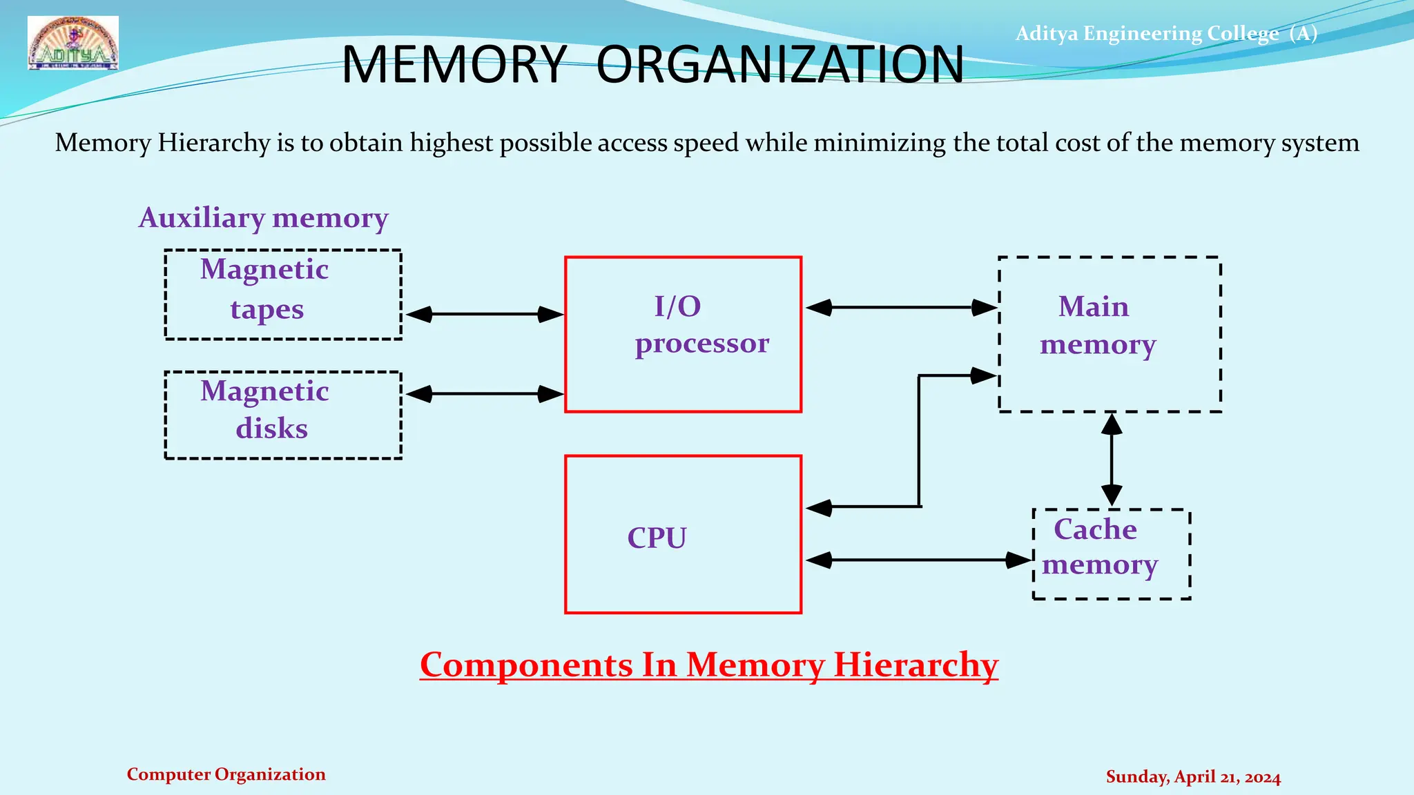
The document provides an overview of memory organization in computer systems, detailing various types of memory such as main memory, auxiliary memory, and cache memory, as well as their hierarchies and architectures. It also discusses key concepts like associative memory, cache performance, and virtual memory management, including address mapping and paging. Additionally, techniques for improving memory access speeds and algorithms for cache memory management are covered.


![Aditya Engineering College (A)
Computer Organization Sunday, April 21, 2024
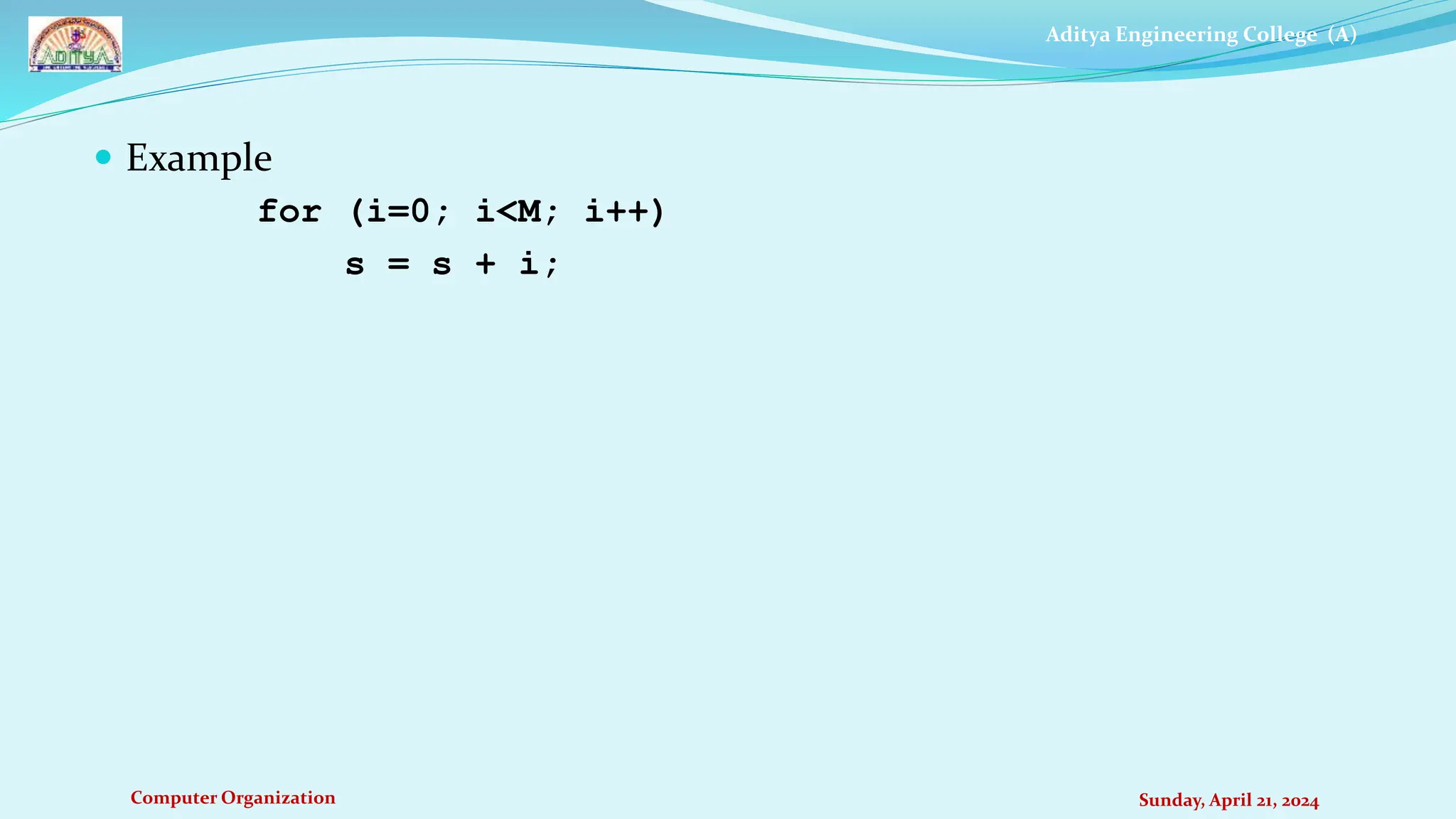
Example
for (i=0; i<M; i++)
for(j=0; j<N; j++)
X[i][j] = X[i][j] + K;
Each element of X is double (eight bytes)
Loop is executed (M*N) times
Placing the code in cache avoids access to main memory
Repetitive use (one of the factors)
Temporal locality
Prefetching data
Spatial locality](https://image.slidesharecdn.com/aecapptcoivsemunit4-240421061233-3922ed8c/75/memory-Organization-in-computer-organization-41-2048.jpg)