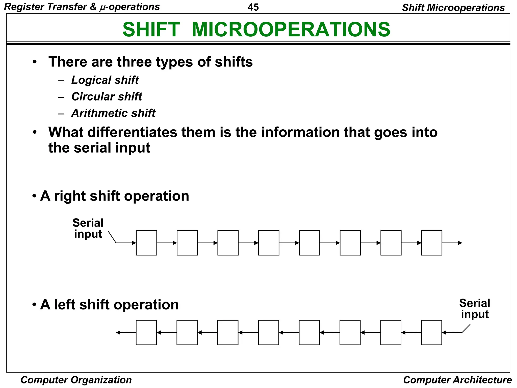
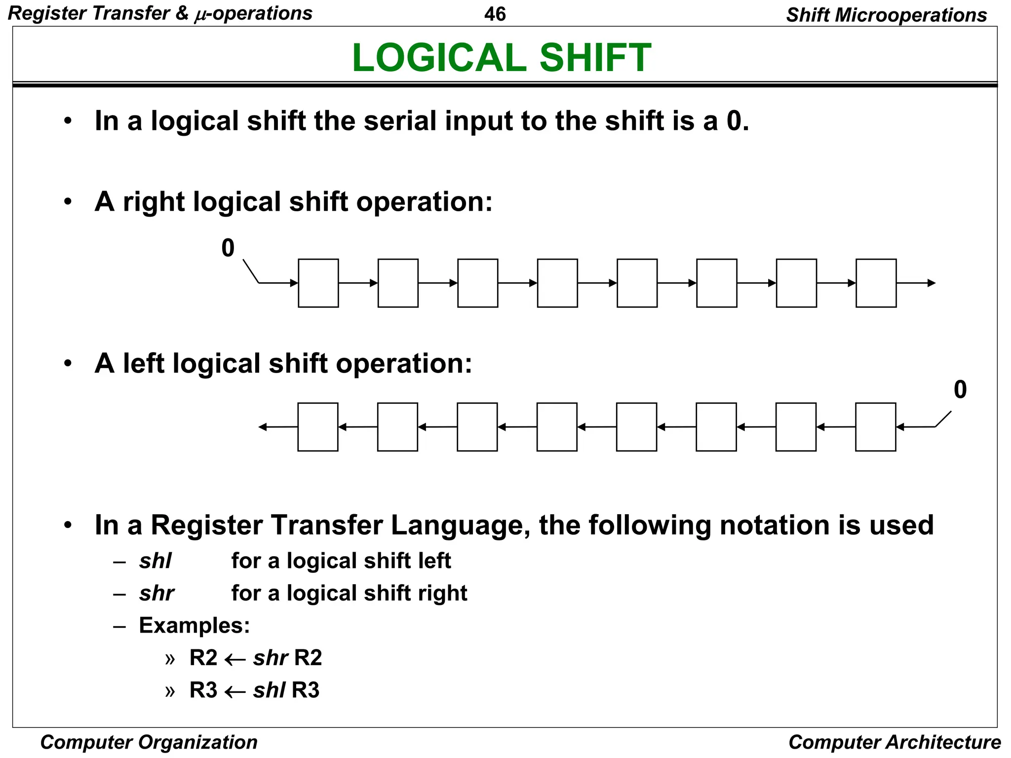
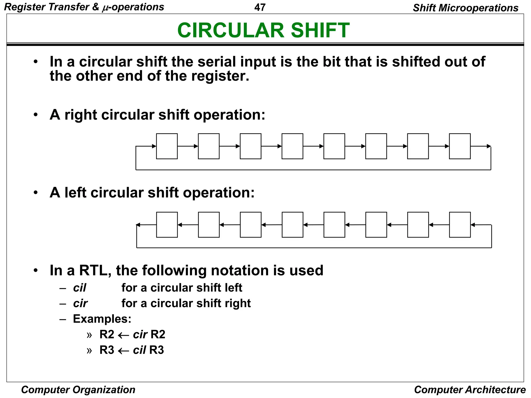
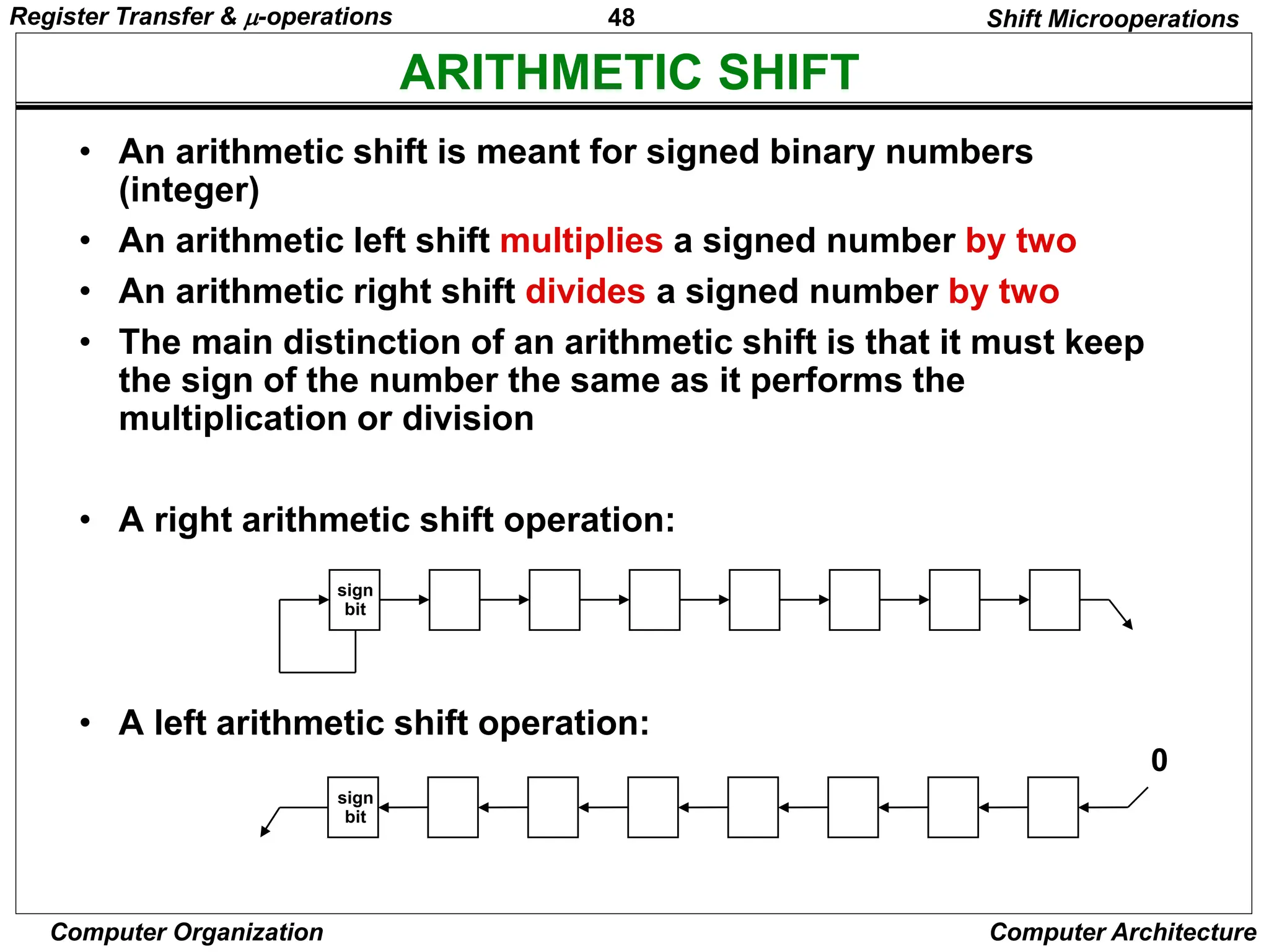
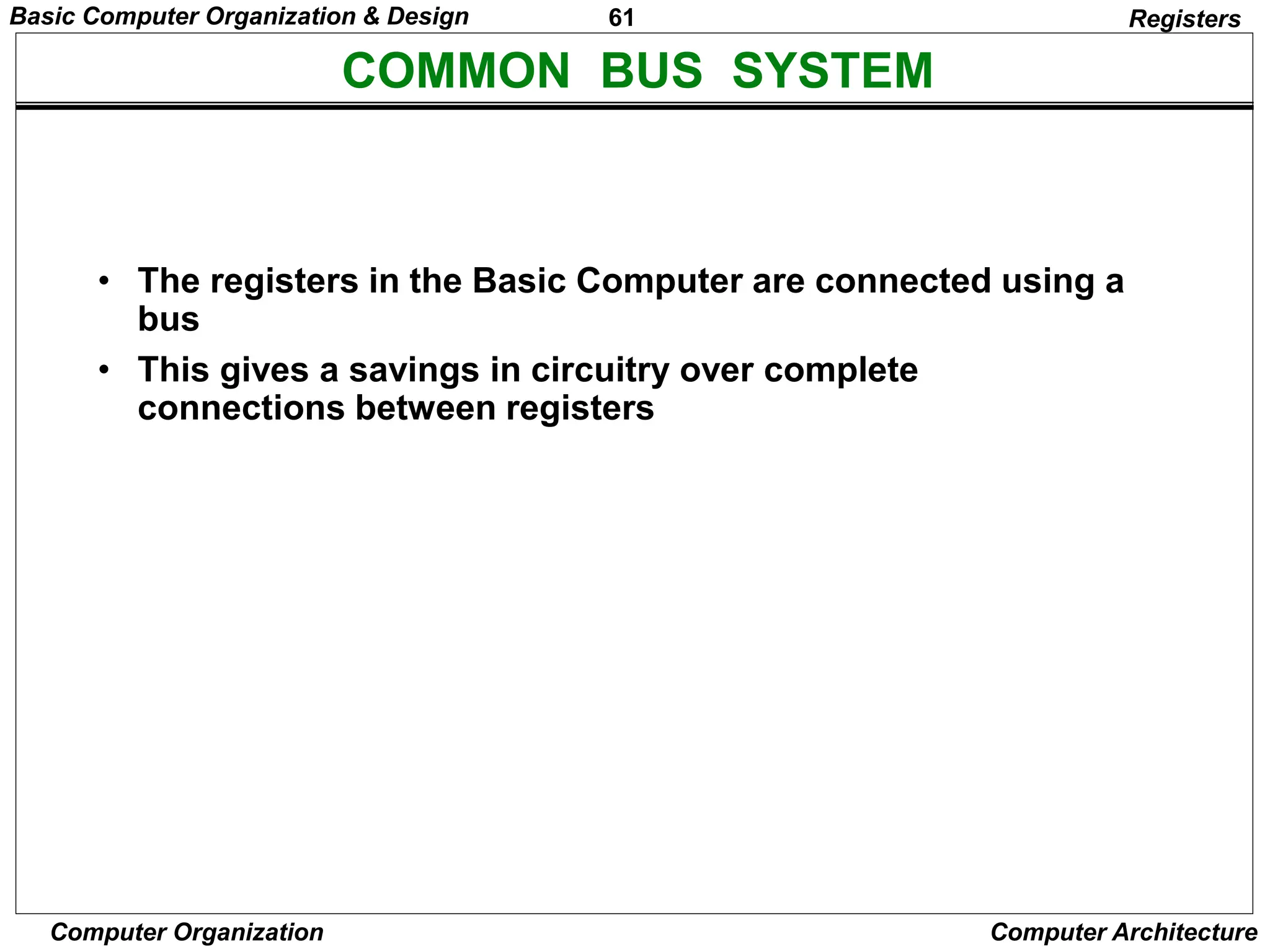
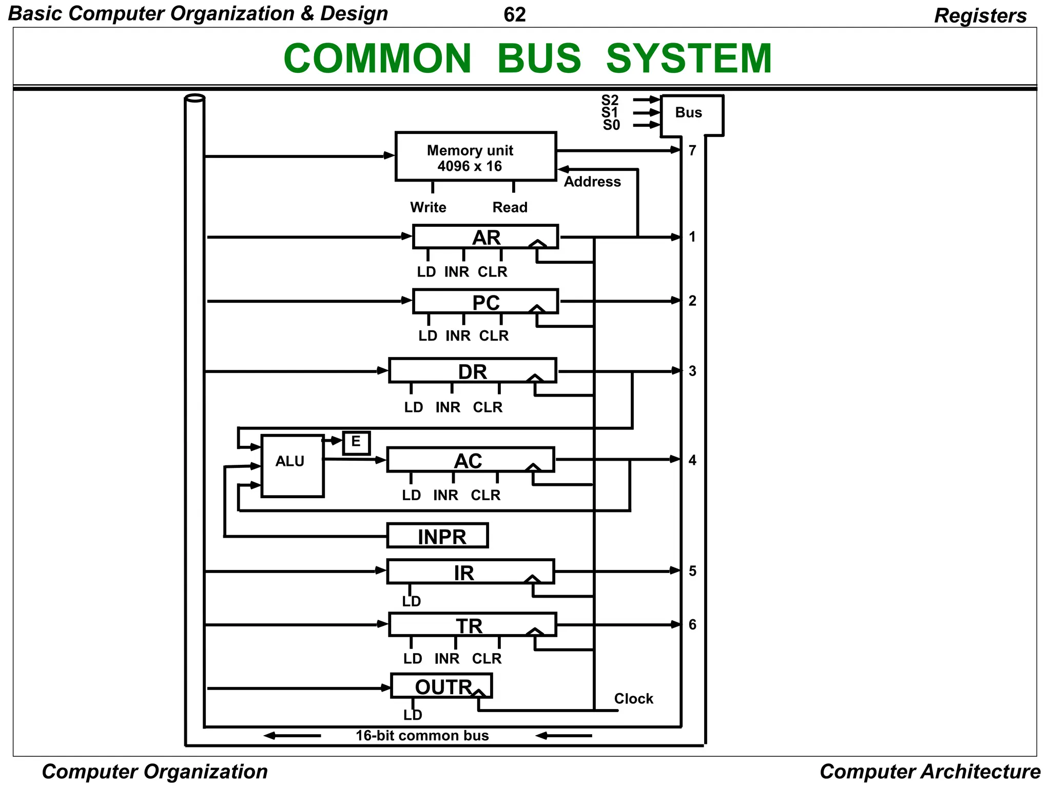
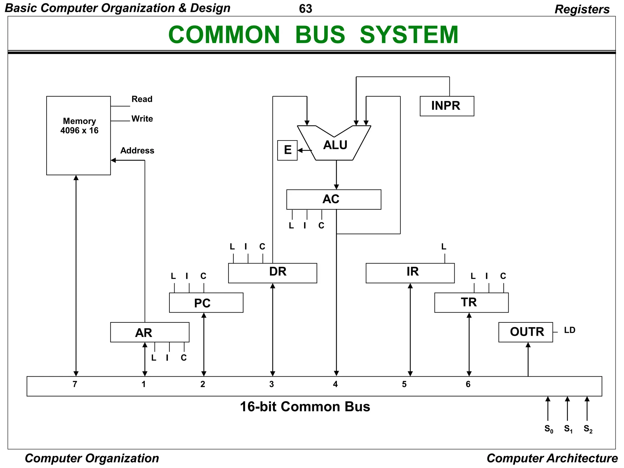
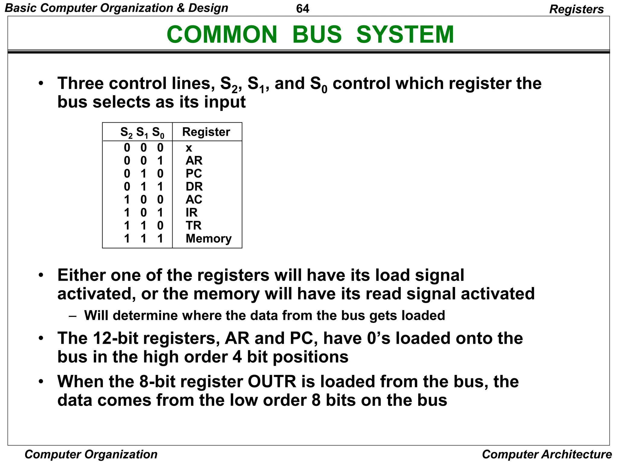
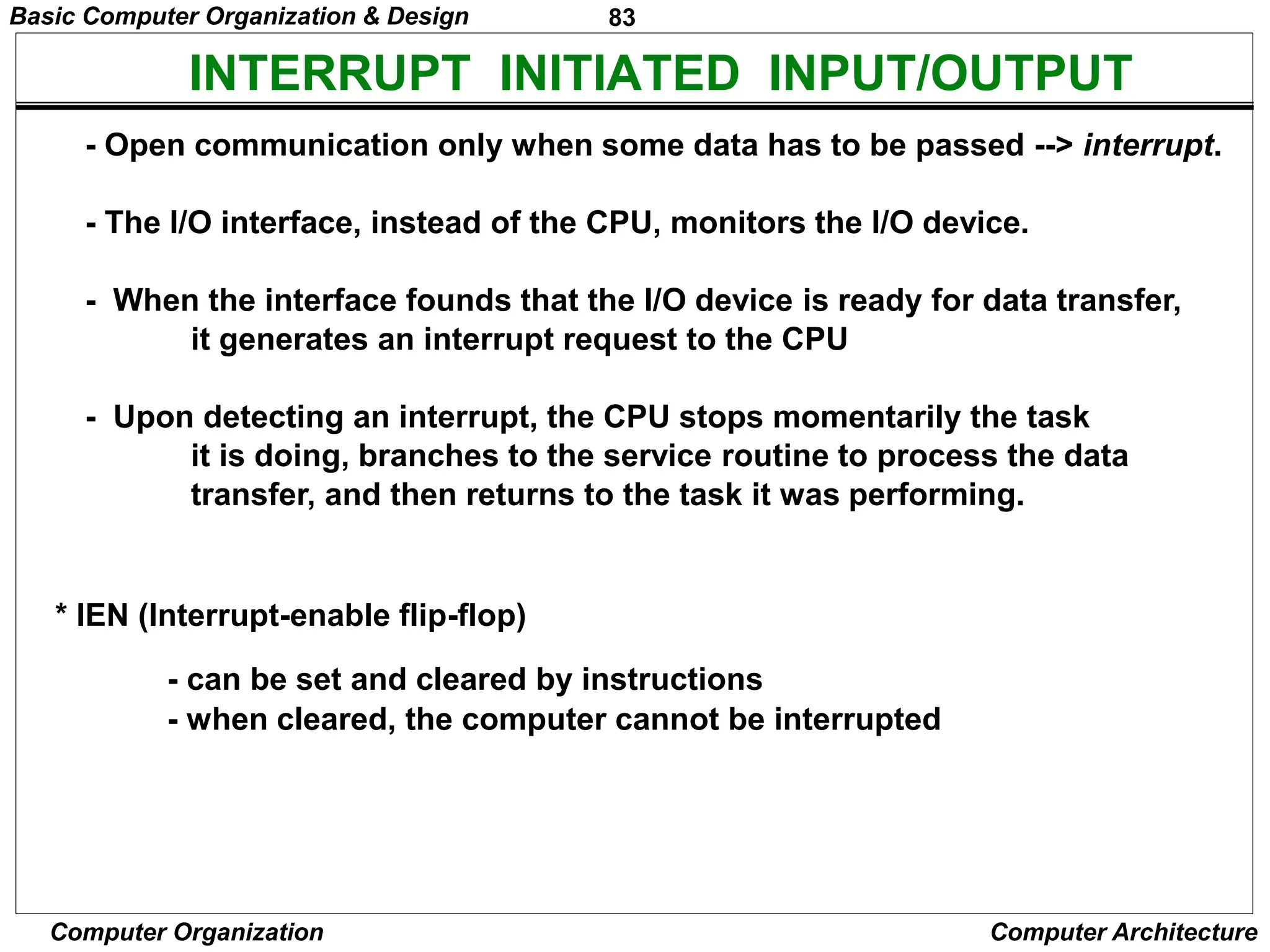
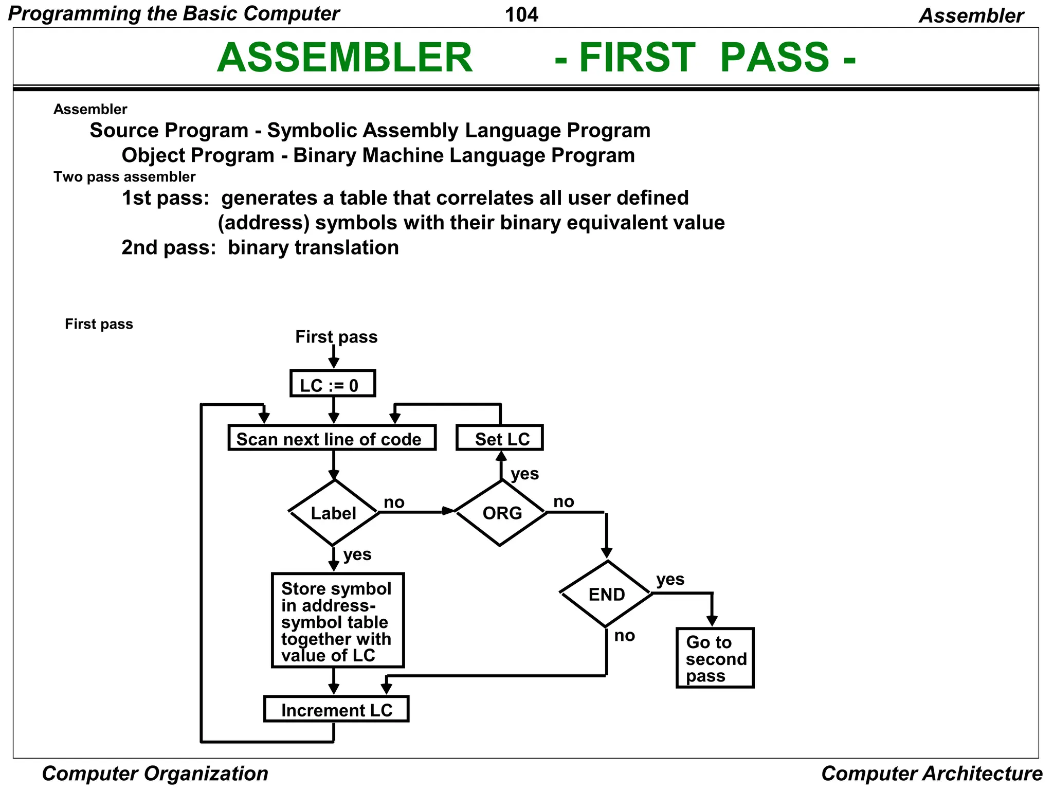
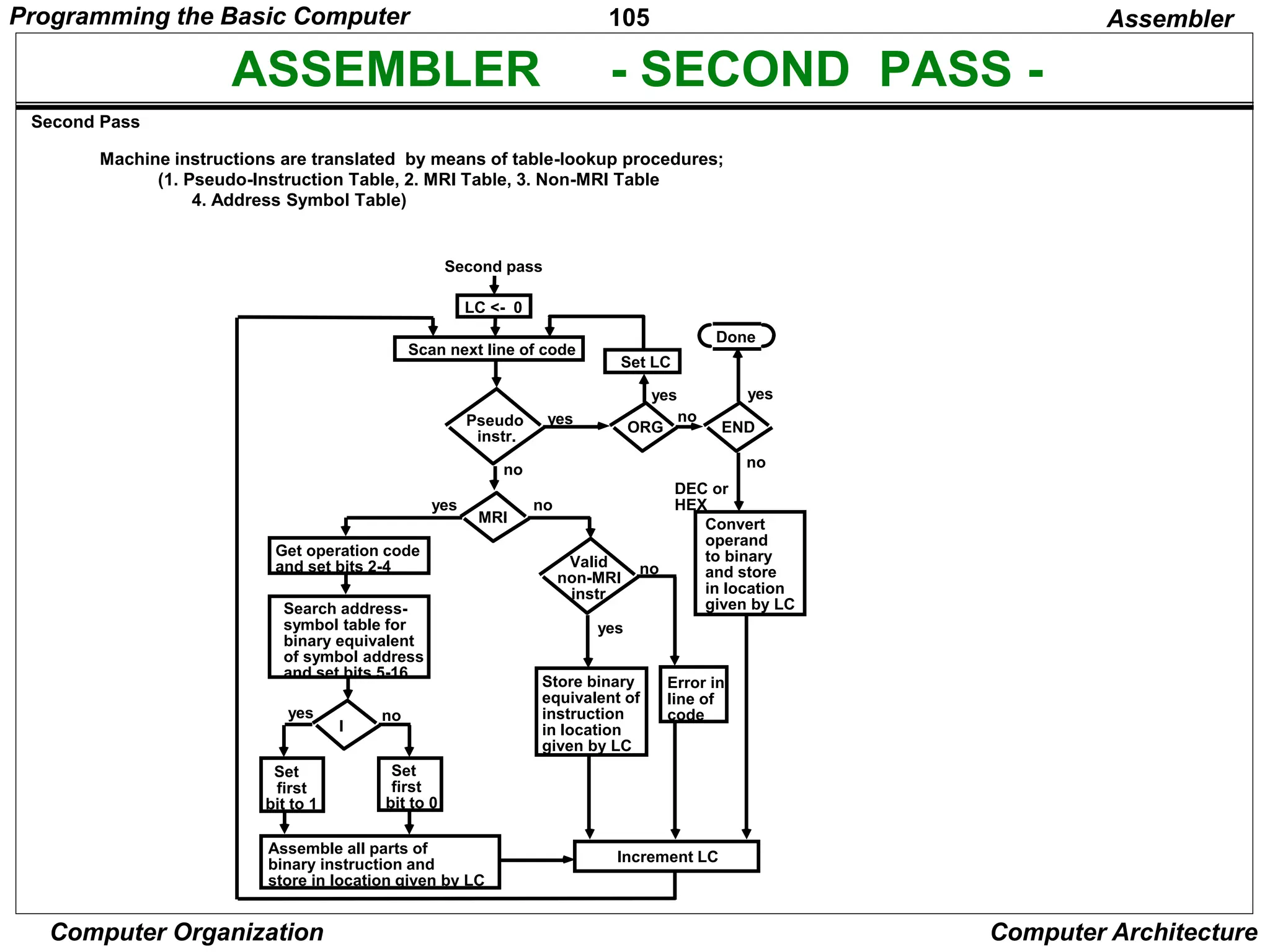
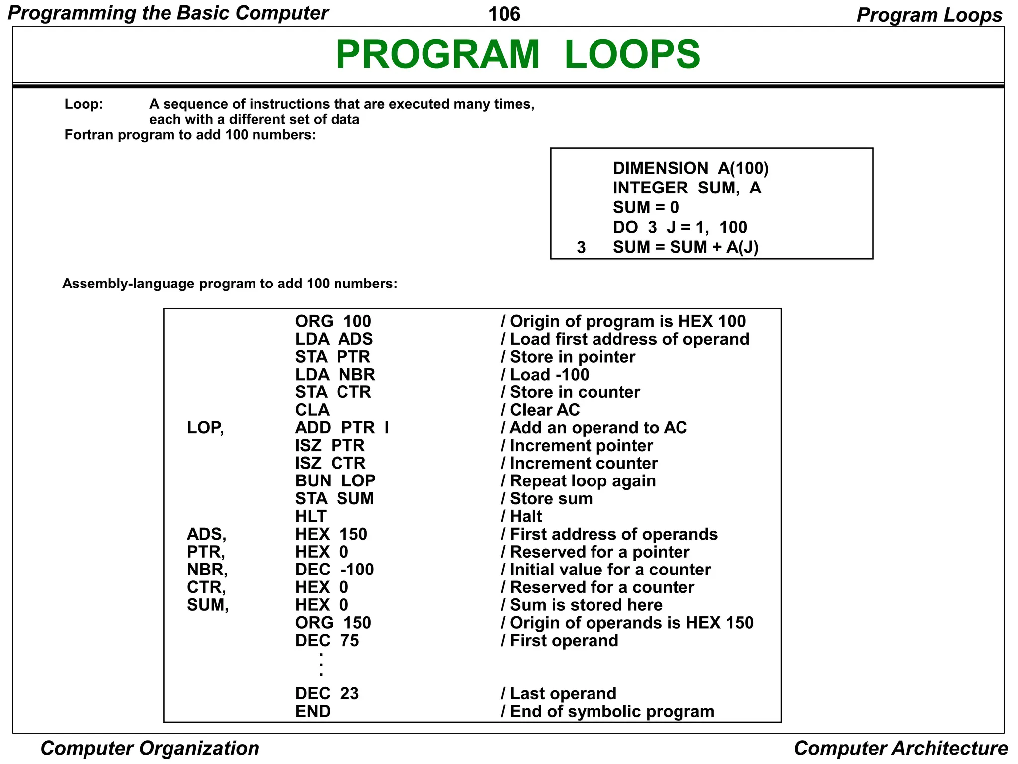
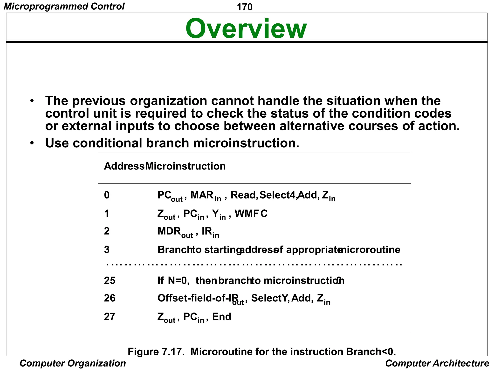
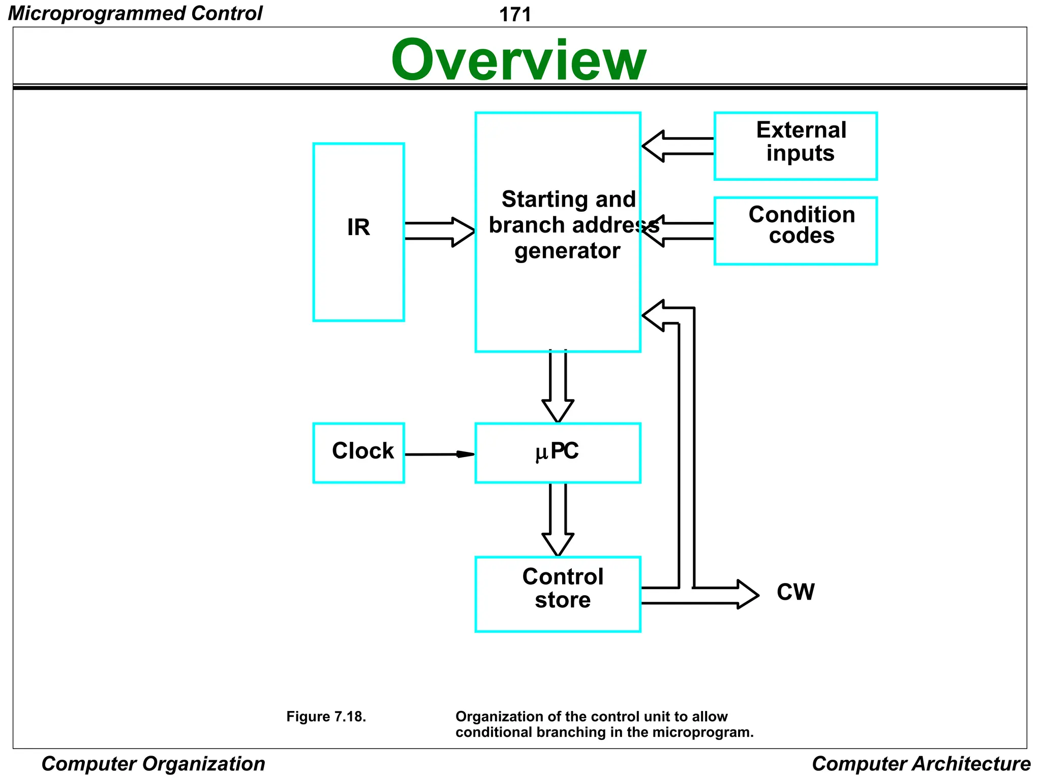
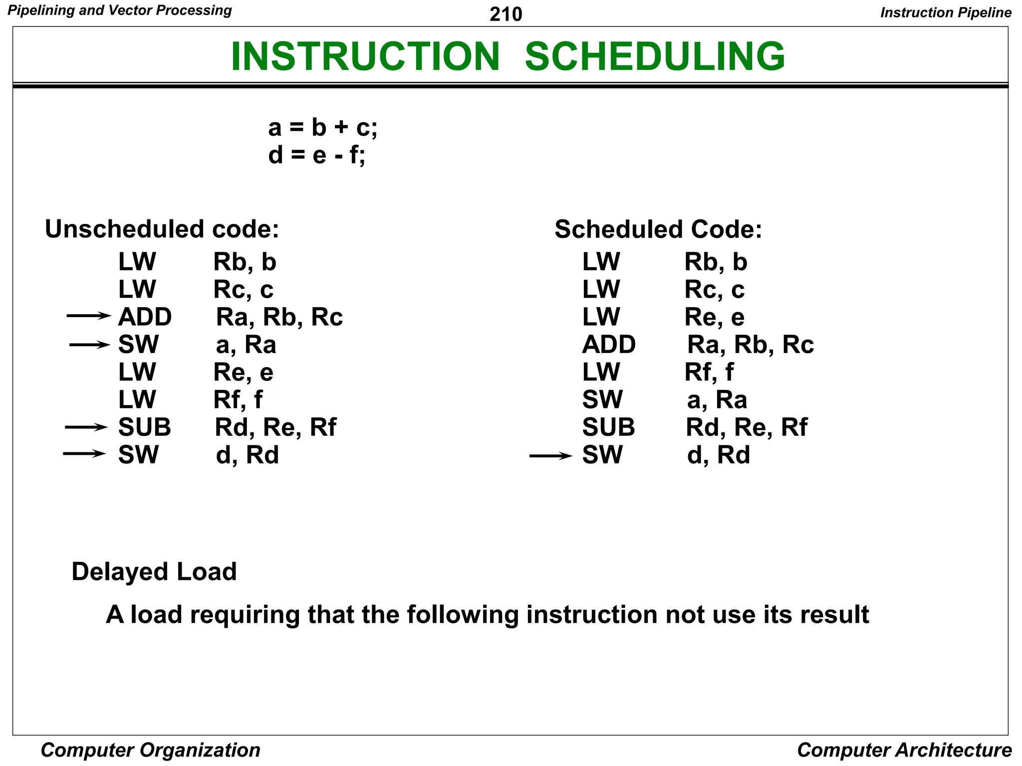
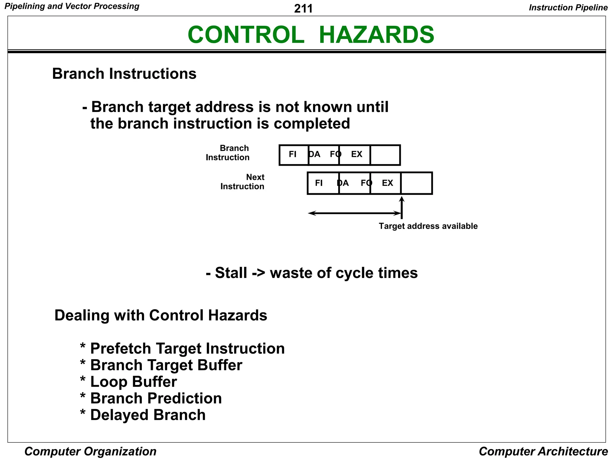
The document outlines various topics within computer organization and architecture, covering digital logic circuits, data representation, and microoperations. It includes chapters on basic computer design, programming, control units, and memory organization, along with detailed explanations of register transfer language and microoperations. Additionally, it discusses arithmetic operations, input-output organization, and multiple processor characteristics, emphasizing the structure and functionality of digital systems.

![28
Computer Organization Computer Architecture
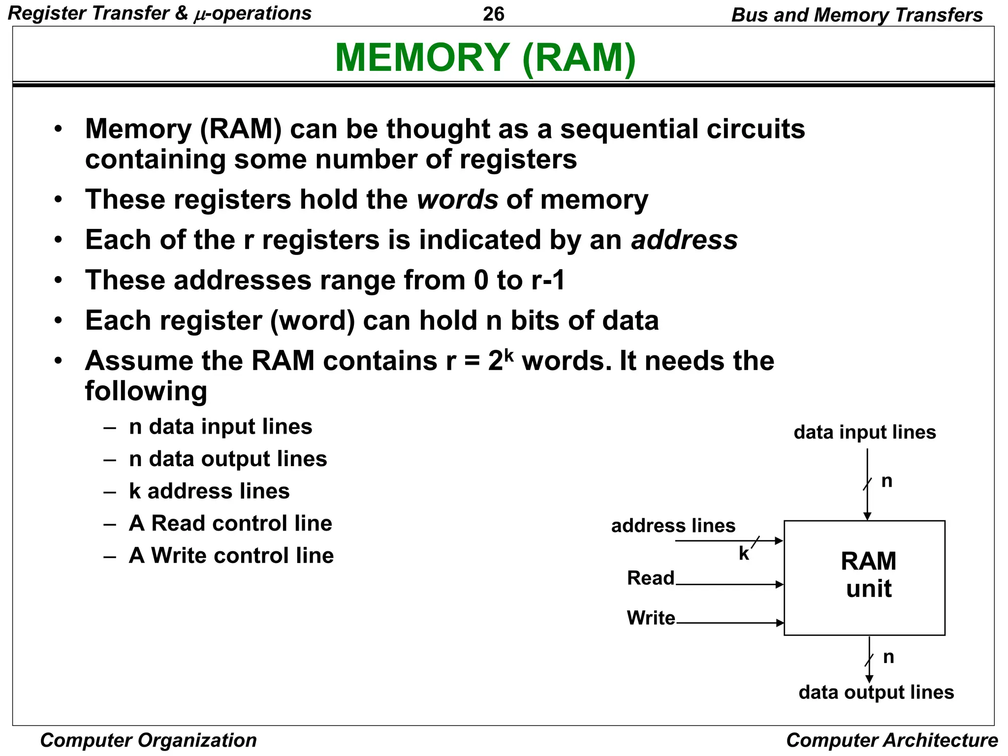
MEMORY READ
Bus and Memory Transfers
• To read a value from a location in memory and load it into
a register, the register transfer language notation looks
like this:
• This causes the following to occur
– The contents of the MAR get sent to the memory address lines
– A Read (= 1) gets sent to the memory unit
– The contents of the specified address are put on the memory’s
output data lines
– These get sent over the bus to be loaded into register R1
R1 M[MAR]
Register Transfer & -operations](https://image.slidesharecdn.com/computer-system-architecture-morris-mano-220720124304-fefd641d-240725153218-d7339dd3/75/computer-system-architecture-morris-mano-220720124304-fefd641d-ppt-28-2048.jpg)
![29
Computer Organization Computer Architecture
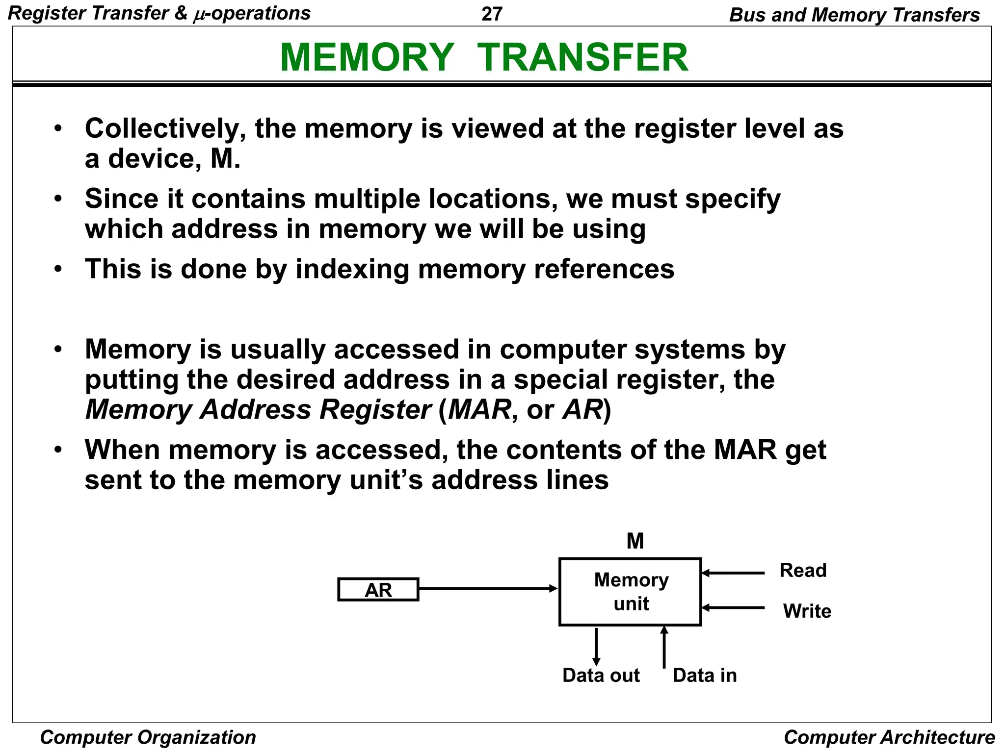
MEMORY WRITE
Bus and Memory Transfers
• To write a value from a register to a location in memory
looks like this in register transfer language:
• This causes the following to occur
– The contents of the MAR get sent to the memory address lines
– A Write (= 1) gets sent to the memory unit
– The values in register R1 get sent over the bus to the data input lines
of the memory
– The values get loaded into the specified address in the memory
M[MAR] R1
Register Transfer & -operations](https://image.slidesharecdn.com/computer-system-architecture-morris-mano-220720124304-fefd641d-240725153218-d7339dd3/75/computer-system-architecture-morris-mano-220720124304-fefd641d-ppt-29-2048.jpg)
![30
Computer Organization Computer Architecture
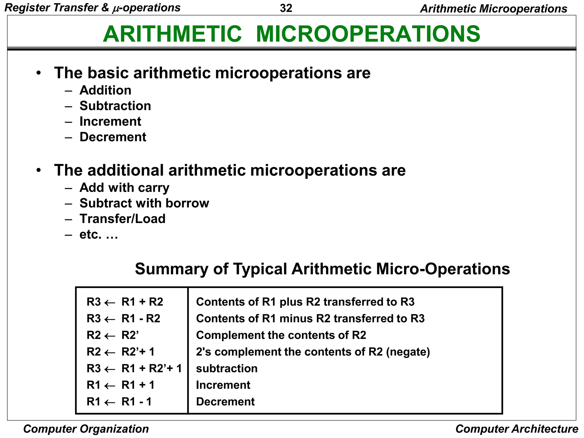
SUMMARY OF R. TRANSFER MICROOPERATIONS
Bus and Memory Transfers
A B Transfer content of reg. B into reg. A
AR DR(AD) Transfer content of AD portion of reg. DR into reg. AR
A constant Transfer a binary constant into reg. A
ABUS R1, Transfer content of R1 into bus A and, at the same time,
R2 ABUS transfer content of bus A into R2
AR Address register
DR Data register
M[R] Memory word specified by reg. R
M Equivalent to M[AR]
DR M Memory read operation: transfers content of
memory word specified by AR into DR
M DR Memory write operation: transfers content of
DR into memory word specified by AR
Register Transfer & -operations](https://image.slidesharecdn.com/computer-system-architecture-morris-mano-220720124304-fefd641d-240725153218-d7339dd3/75/computer-system-architecture-morris-mano-220720124304-fefd641d-ppt-30-2048.jpg)
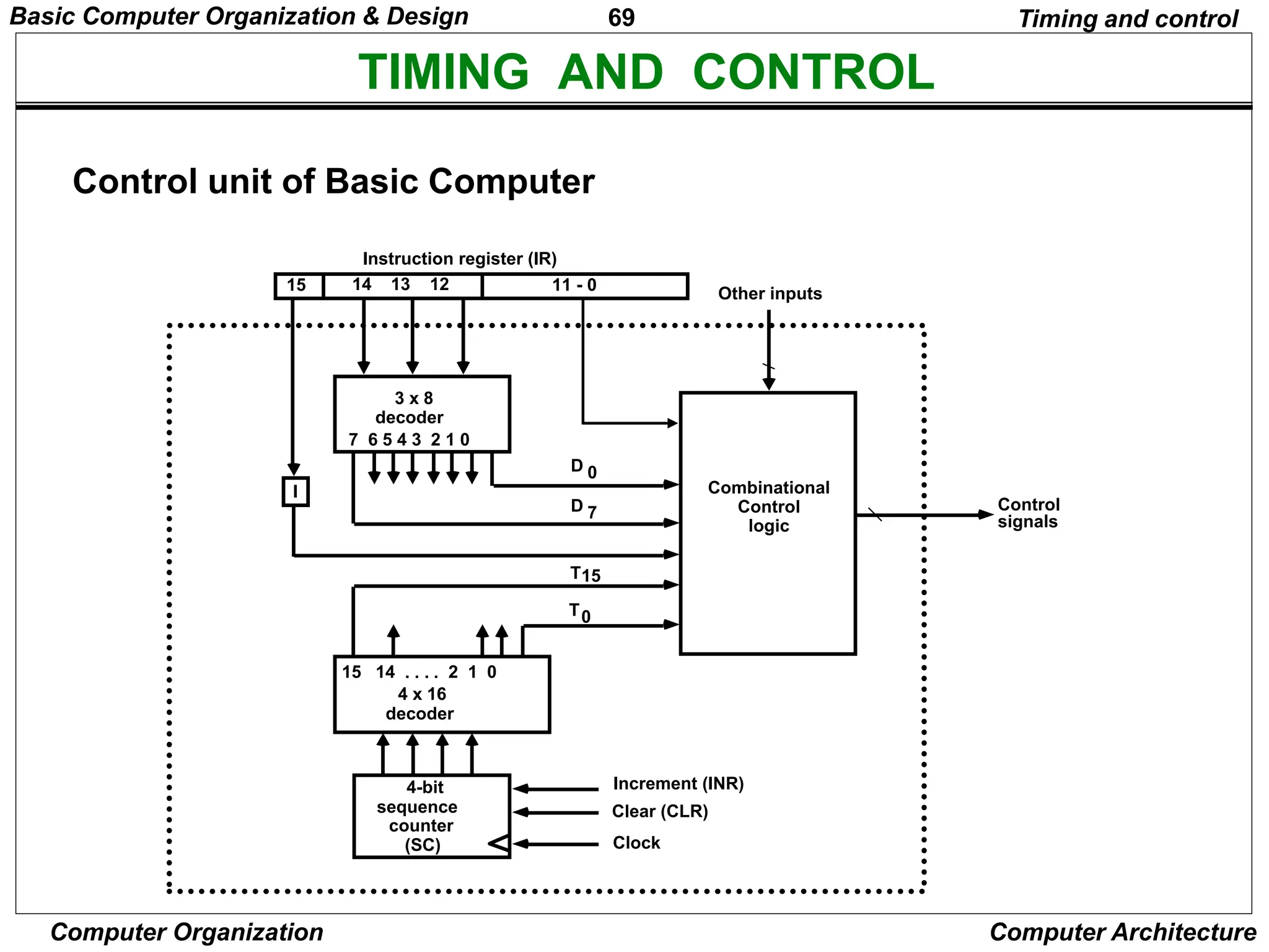
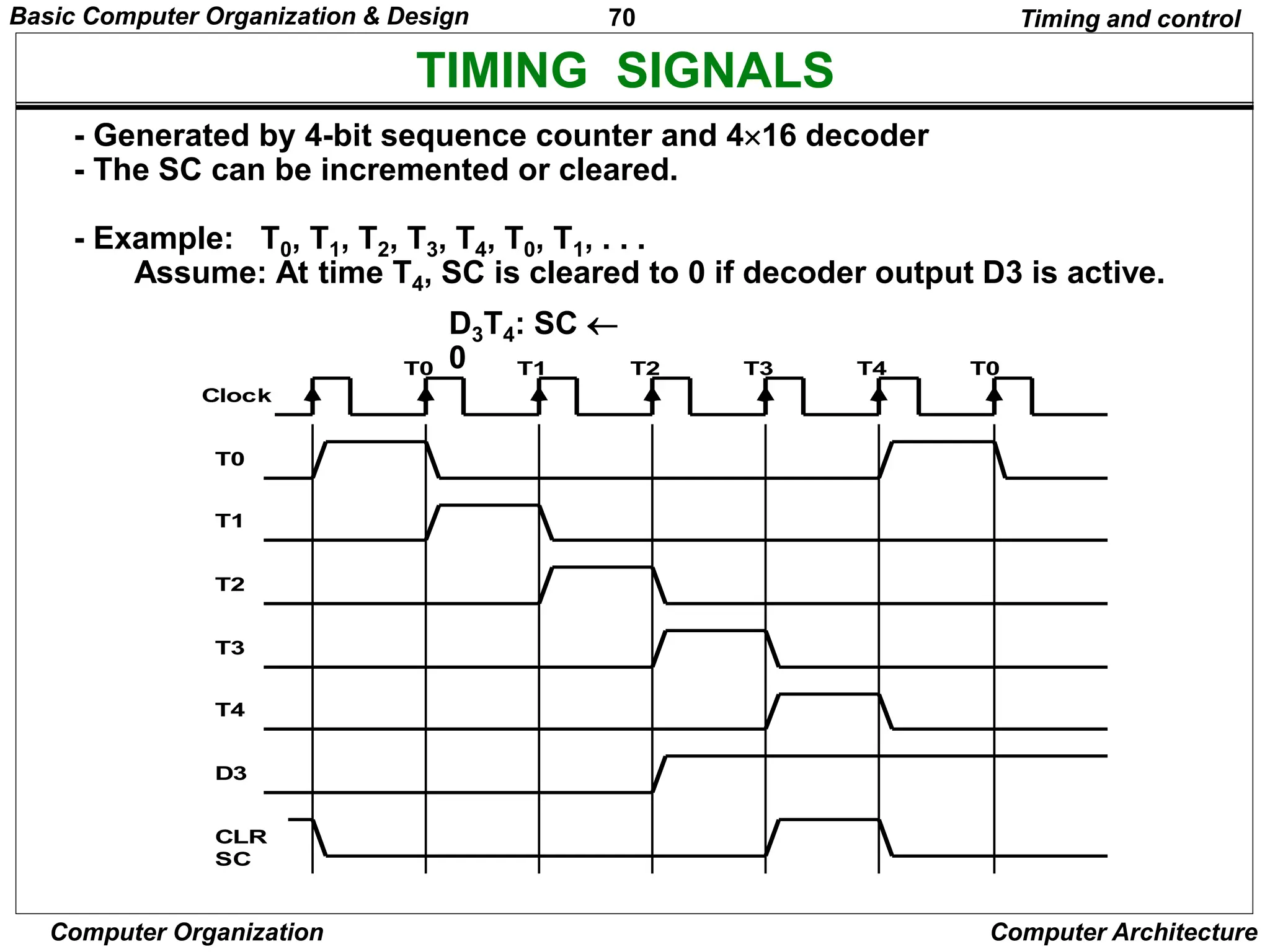
![72
Computer Organization Computer Architecture
FETCH and DECODE
• Fetch and Decode T0: AR PC (S0S1S2=010, T0=1)
T1: IR M [AR], PC PC + 1 (S0S1S2=111, T1=1)
T2: D0, . . . , D7 Decode IR(12-14), AR IR(0-11), I IR(15)
S2
S1
S0
Bus
7
Memory
unit
Address
Read
AR
LD
PC
INR
IR
LD
Clock
1
2
5
Common bus
T1
T0
Instruction Cycle
Basic Computer Organization & Design](https://image.slidesharecdn.com/computer-system-architecture-morris-mano-220720124304-fefd641d-240725153218-d7339dd3/75/computer-system-architecture-morris-mano-220720124304-fefd641d-ppt-72-2048.jpg)
![73
Computer Organization Computer Architecture
DETERMINE THE TYPE OF INSTRUCTION
= 0 (direct)
D'7IT3: AR M[AR]
D'7I'T3: Nothing
D7I'T3: Execute a register-reference instr.
D7IT3: Execute an input-output instr.
Instrction Cycle
Start
SC 0
AR PC
T0
IR M[AR], PC PC + 1
T1
AR IR(0-11), I IR(15)
Decode Opcode in IR(12-14),
T2
D7
= 0 (Memory-reference)
(Register or I/O) = 1
I
I
Execute
register-reference
instruction
SC 0
Execute
input-output
instruction
SC 0
M[AR]
AR Nothing
= 0 (register)
(I/O) = 1 (indirect) = 1
T3 T3 T3 T3
Execute
memory-reference
instruction
SC 0
T4
Basic Computer Organization & Design](https://image.slidesharecdn.com/computer-system-architecture-morris-mano-220720124304-fefd641d-240725153218-d7339dd3/75/computer-system-architecture-morris-mano-220720124304-fefd641d-ppt-73-2048.jpg)
![75
Computer Organization Computer Architecture
MEMORY REFERENCE INSTRUCTIONS
AND to AC
D0T4: DR M[AR] Read operand
D0T5: AC AC DR, SC 0 AND with AC
ADD to AC
D1T4: DR M[AR] Read operand
D1T5: AC AC + DR, E Cout, SC 0 Add to AC and store carry in E
- The effective address of the instruction is in AR and was placed there during
timing signal T2 when I = 0, or during timing signal T3 when I = 1
- Memory cycle is assumed to be short enough to complete in a CPU cycle
- The execution of MR instruction starts with T4
MR Instructions
Symbol
Operation
Decoder Symbolic Description
AND D0 AC AC M[AR]
ADD D1 AC AC + M[AR], E Cout
LDA D2 AC M[AR]
STA D3 M[AR] AC
BUN D4 PC AR
BSA D5 M[AR] PC, PC AR + 1
ISZ D6 M[AR] M[AR] + 1, if M[AR] + 1 = 0 then PC PC+1
Basic Computer Organization & Design](https://image.slidesharecdn.com/computer-system-architecture-morris-mano-220720124304-fefd641d-240725153218-d7339dd3/75/computer-system-architecture-morris-mano-220720124304-fefd641d-ppt-75-2048.jpg)
![76
Computer Organization Computer Architecture
MEMORY REFERENCE INSTRUCTIONS
Memory, PC after execution
21
0 BSA 135
Next instruction
Subroutine
20
PC = 21
AR = 135
136
1 BUN 135
Memory, PC, AR at time T4
0 BSA 135
Next instruction
Subroutine
20
21
135
PC = 136
1 BUN 135
Memory Memory
LDA: Load to AC
D2T4: DR M[AR]
D2T5: AC DR, SC 0
STA: Store AC
D3T4: M[AR] AC, SC 0
BUN: Branch Unconditionally
D4T4: PC AR, SC 0
BSA: Branch and Save Return Address
M[AR] PC, PC AR + 1
Basic Computer Organization & Design](https://image.slidesharecdn.com/computer-system-architecture-morris-mano-220720124304-fefd641d-240725153218-d7339dd3/75/computer-system-architecture-morris-mano-220720124304-fefd641d-ppt-76-2048.jpg)
![77
Computer Organization Computer Architecture
MEMORY REFERENCE INSTRUCTIONS
MR Instructions
BSA:
D5T4: M[AR] PC, AR AR + 1
D5T5: PC AR, SC 0
ISZ: Increment and Skip-if-Zero
D6T4: DR M[AR]
D6T5: DR DR + 1
D6T4: M[AR] DR, if (DR = 0) then (PC PC + 1), SC 0
Basic Computer Organization & Design](https://image.slidesharecdn.com/computer-system-architecture-morris-mano-220720124304-fefd641d-240725153218-d7339dd3/75/computer-system-architecture-morris-mano-220720124304-fefd641d-ppt-77-2048.jpg)
![78
Computer Organization Computer Architecture
FLOWCHART FOR MEMORY REFERENCE INSTRUCTIONS
MR Instructions
Memory-reference instruction
DR M[AR] DR M[AR] DR M[AR] M[AR] AC
SC 0
AND ADD LDA STA
AC AC DR
SC 0
AC AC + DR
E Cout
SC 0
AC DR
SC 0
D T
0 4 D T
1 4 D T
2 4 D T
3 4
D T
0 5 D T
1 5 D T
2 5
PC AR
SC 0
M[AR] PC
AR AR + 1
DR M[AR]
BUN BSA ISZ
D T
4 4 D T
5 4 D T
6 4
DR DR + 1
D T
5 5 D T
6 5
PC AR
SC 0
M[AR] DR
If (DR = 0)
then (PC PC + 1)
SC 0
D T
6 6
Basic Computer Organization & Design](https://image.slidesharecdn.com/computer-system-architecture-morris-mano-220720124304-fefd641d-240725153218-d7339dd3/75/computer-system-architecture-morris-mano-220720124304-fefd641d-ppt-78-2048.jpg)
![84
Computer Organization Computer Architecture
FLOWCHART FOR INTERRUPT CYCLE
R = Interrupt f/f
- The interrupt cycle is a HW implementation of a branch
and save return address operation.
- At the beginning of the next instruction cycle, the
instruction that is read from memory is in address 1.
- At memory address 1, the programmer must store a branch instruction
that sends the control to an interrupt service routine
- The instruction that returns the control to the original
program is "indirect BUN 0"
I/O and Interrupt
Store return address
R
=1
=0
in location 0
M[0] PC
Branch to location 1
PC 1
IEN 0
R 0
Interrupt cycle
Instruction cycle
Fetch and decode
instructions
IEN
FGI
FGO
Execute
instructions
R 1
=1
=1
=1
=0
=0
=0
Basic Computer Organization & Design](https://image.slidesharecdn.com/computer-system-architecture-morris-mano-220720124304-fefd641d-240725153218-d7339dd3/75/computer-system-architecture-morris-mano-220720124304-fefd641d-ppt-84-2048.jpg)
![85
Computer Organization Computer Architecture
REGISTER TRANSFER OPERATIONS IN INTERRUPT CYCLE
Register Transfer Statements for Interrupt Cycle
- R F/F 1 if IEN (FGI + FGO)T0T1T2
T0T1T2 (IEN)(FGI + FGO): R 1
- The fetch and decode phases of the instruction cycle
must be modified Replace T0, T1, T2 with R'T0, R'T1, R'T2
- The interrupt cycle :
RT0: AR 0, TR PC
RT1: M[AR] TR, PC 0
RT2: PC PC + 1, IEN 0, R 0, SC 0
After interrupt cycle
0 BUN 1120
0
1
PC = 256
255
1 BUN 0
Before interrupt
Main
Program
1120
I/O
Program
0 BUN 1120
0
PC = 1
256
255
1 BUN 0
Memory
Main
Program
1120
I/O
Program
256
I/O and Interrupt
Basic Computer Organization & Design](https://image.slidesharecdn.com/computer-system-architecture-morris-mano-220720124304-fefd641d-240725153218-d7339dd3/75/computer-system-architecture-morris-mano-220720124304-fefd641d-ppt-85-2048.jpg)
![87
Computer Organization Computer Architecture
COMPLETE COMPUTER DESCRIPTION
Flowchart of Operations
Description
=1 (I/O) =0 (Register) =1(Indir) =0(Dir)
start
SC 0, IEN 0, R 0
R
AR PC
R’T0
IR M[AR], PC PC + 1
R’T1
AR IR(0~11), I IR(15)
D0...D7 Decode IR(12 ~ 14)
R’T2
AR 0, TR PC
RT0
M[AR] TR, PC 0
RT1
PC PC + 1, IEN 0
R 0, SC 0
RT2
D7
I I
Execute
I/O
Instruction
Execute
RR
Instruction
AR <- M[AR] Idle
D7IT3 D7I’T3 D7’IT3 D7’I’T3
Execute MR
Instruction
=0(Instruction =1(Interrupt
Cycle) Cycle)
=1(Register or I/O) =0(Memory Ref)
D7’T4
Basic Computer Organization & Design](https://image.slidesharecdn.com/computer-system-architecture-morris-mano-220720124304-fefd641d-240725153218-d7339dd3/75/computer-system-architecture-morris-mano-220720124304-fefd641d-ppt-87-2048.jpg)
![88
Computer Organization Computer Architecture
COMPLETE COMPUTER DESCRIPTION
Microoperations
Description
Fetch
Decode
Indirect
Interrupt
Memory-Reference
AND
ADD
LDA
STA
BUN
BSA
ISZ
RT0:
RT1:
RT2:
D7IT3:
RT0:
RT1:
RT2:
D0T4:
D0T5:
D1T4:
D1T5:
D2T4:
D2T5:
D3T4:
D4T4:
D5T4:
D5T5:
D6T4:
D6T5:
D6T6:
AR PC
IR M[AR], PC PC + 1
D0, ..., D7 Decode IR(12 ~ 14),
AR IR(0 ~ 11), I IR(15)
AR M[AR]
R 1
AR 0, TR PC
M[AR] TR, PC 0
PC PC + 1, IEN 0, R 0, SC 0
DR M[AR]
AC AC DR, SC 0
DR M[AR]
AC AC + DR, E Cout, SC 0
DR M[AR]
AC DR, SC 0
M[AR] AC, SC 0
PC AR, SC 0
M[AR] PC, AR AR + 1
PC AR, SC 0
DR M[AR]
DR DR + 1
M[AR] DR, if(DR=0) then (PC PC + 1),
SC 0
T0T1T2(IEN)(FGI + FGO):
Basic Computer Organization & Design](https://image.slidesharecdn.com/computer-system-architecture-morris-mano-220720124304-fefd641d-240725153218-d7339dd3/75/computer-system-architecture-morris-mano-220720124304-fefd641d-ppt-88-2048.jpg)
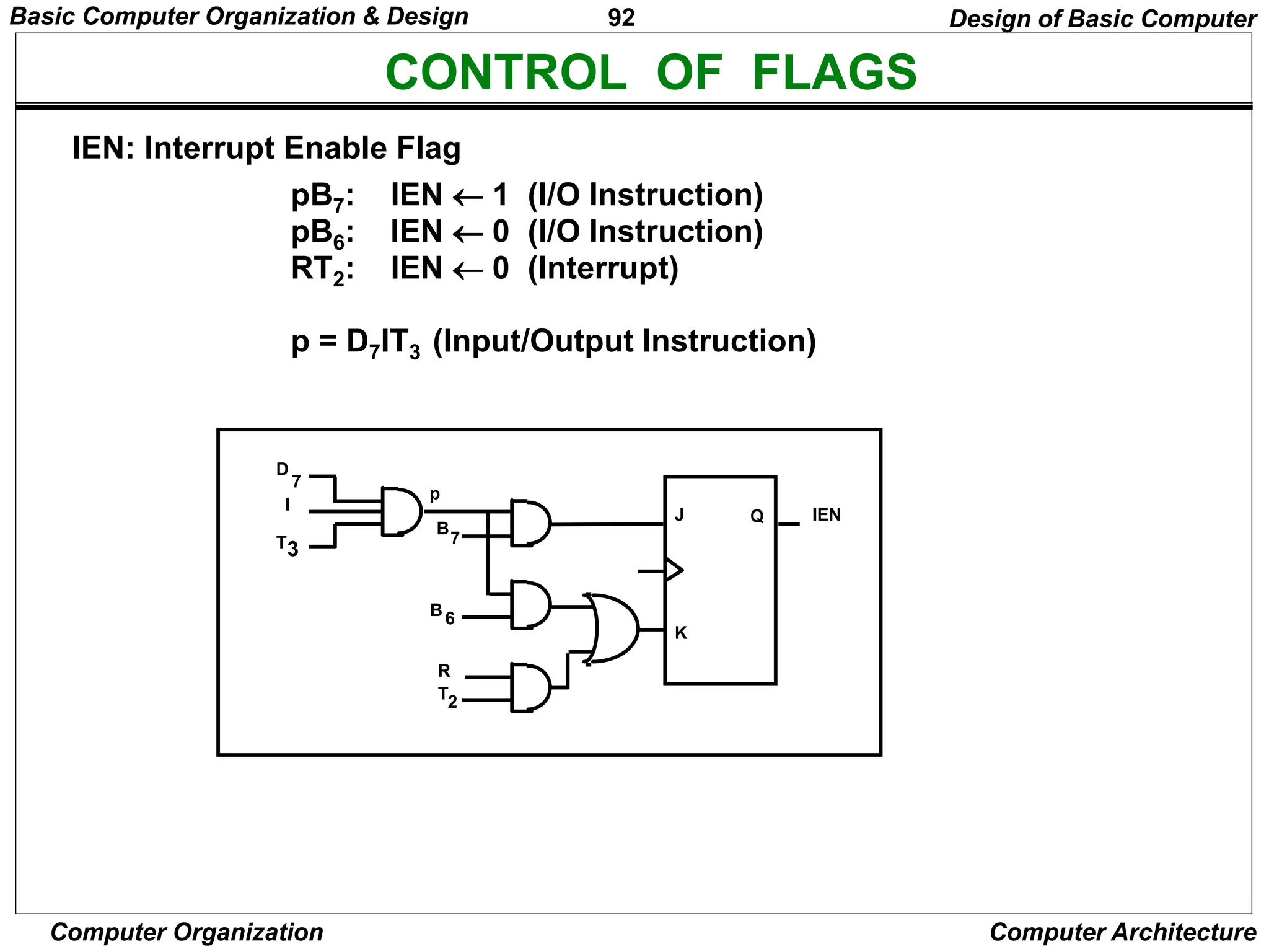
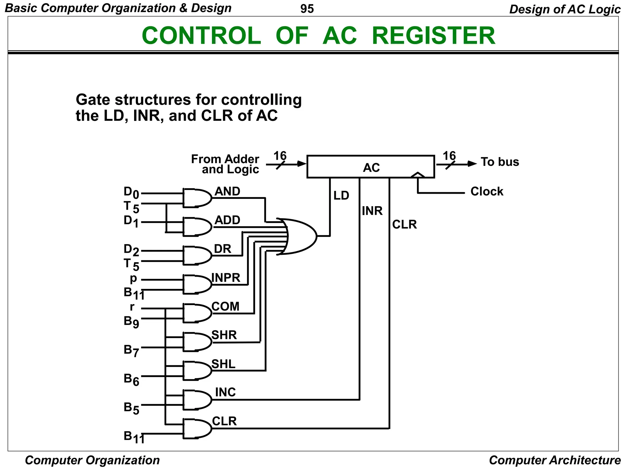
![91
Computer Organization Computer Architecture
CONTROL OF REGISTERS AND MEMORY
Scan all of the register transfer statements that change the content of AR:
LD(AR) = R'T0 + R'T2 + D'7IT3
CLR(AR) = RT0
INR(AR) = D5T4
Address Register; AR
R’T0: AR PC LD(AR)
R’T2: AR IR(0-11) LD(AR)
D’7IT3: AR M[AR] LD(AR)
RT0: AR 0 CLR(AR)
D5T4: AR AR + 1 INR(AR)
Design of Basic Computer
AR
LD
INR
CLR
Clock
To bus
12
From bus
12
D'
I
T
T
R
T
D
T
7
3
2
0
4
Basic Computer Organization & Design](https://image.slidesharecdn.com/computer-system-architecture-morris-mano-220720124304-fefd641d-240725153218-d7339dd3/75/computer-system-architecture-morris-mano-220720124304-fefd641d-ppt-91-2048.jpg)
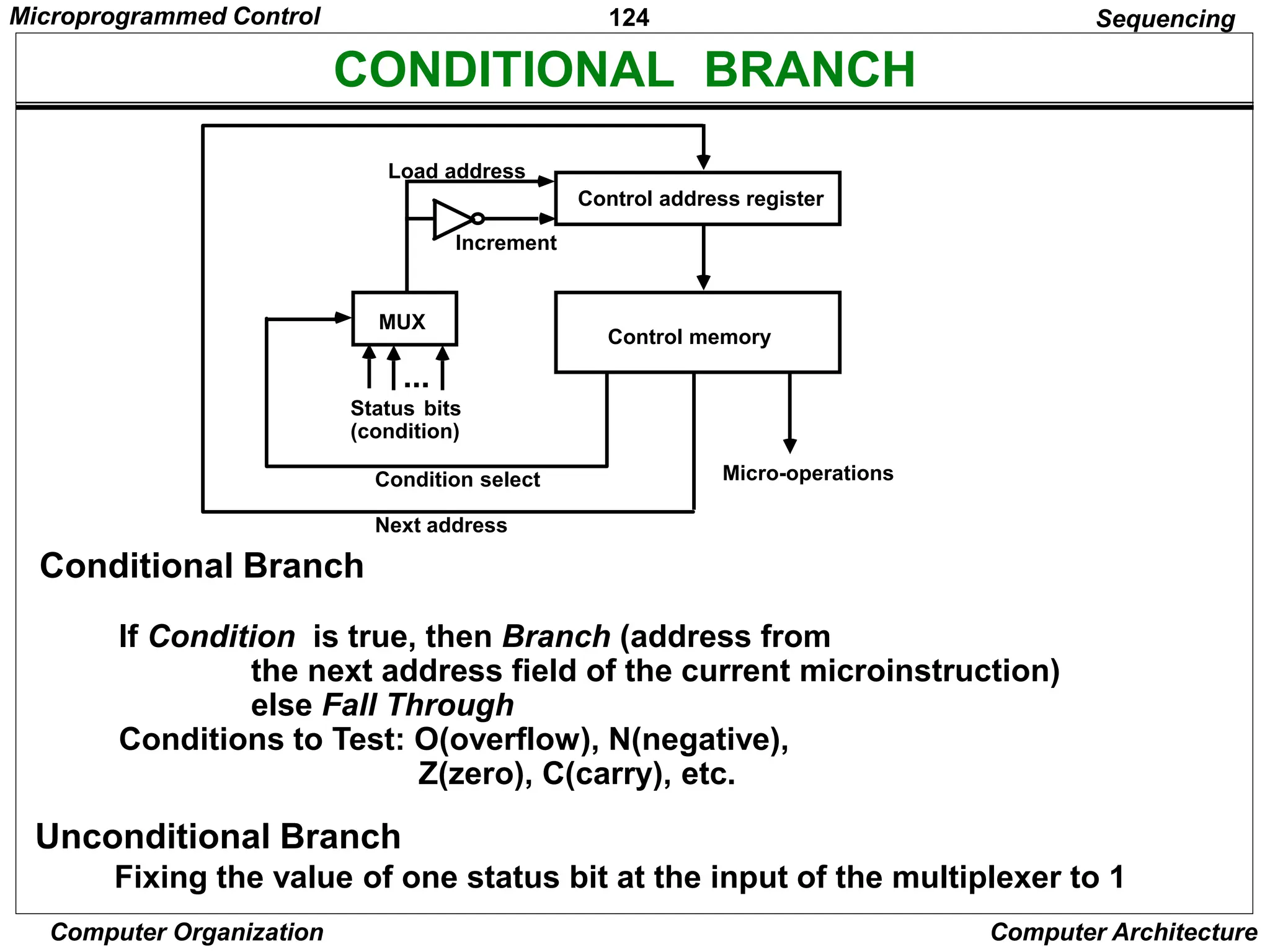
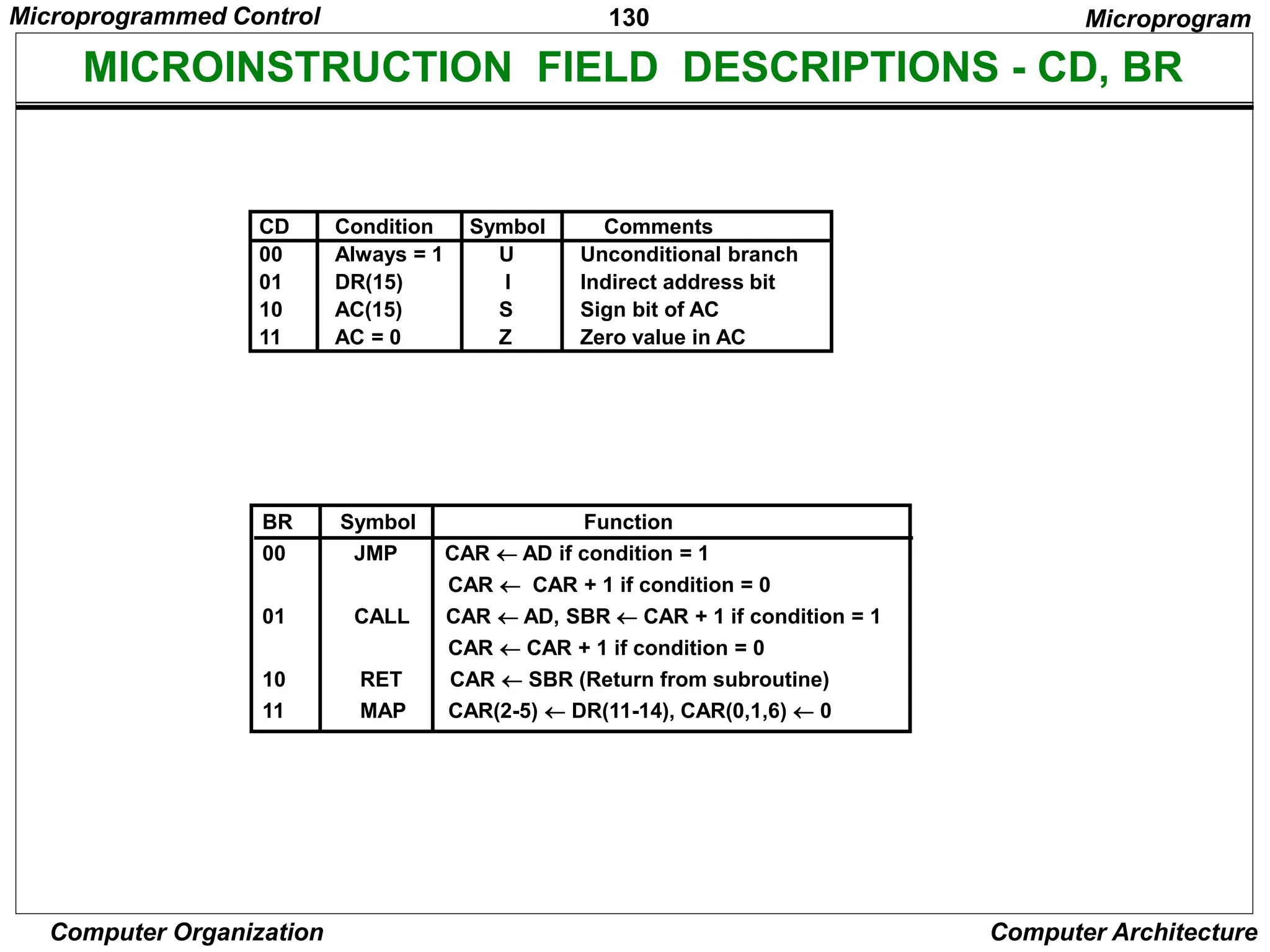
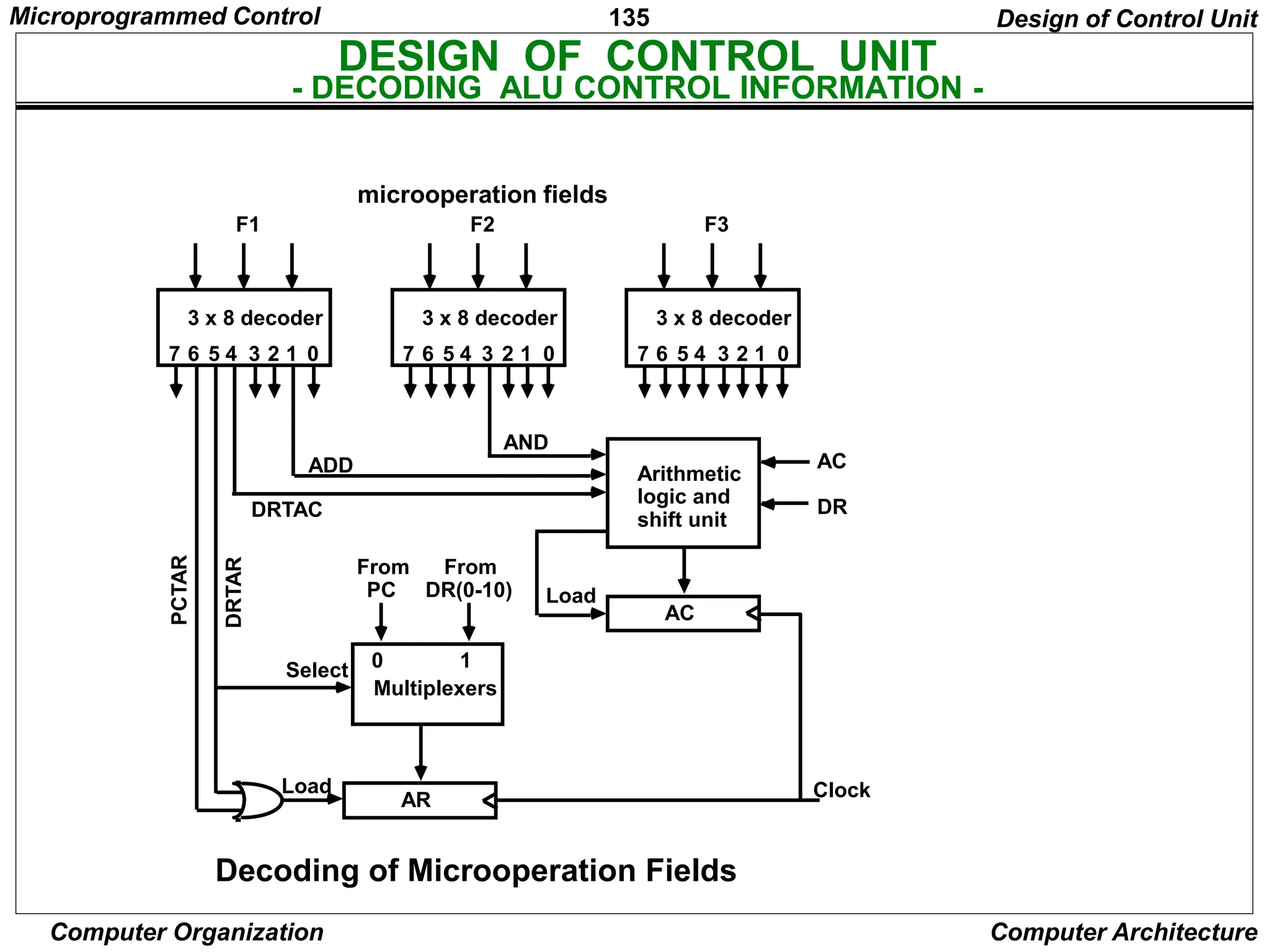
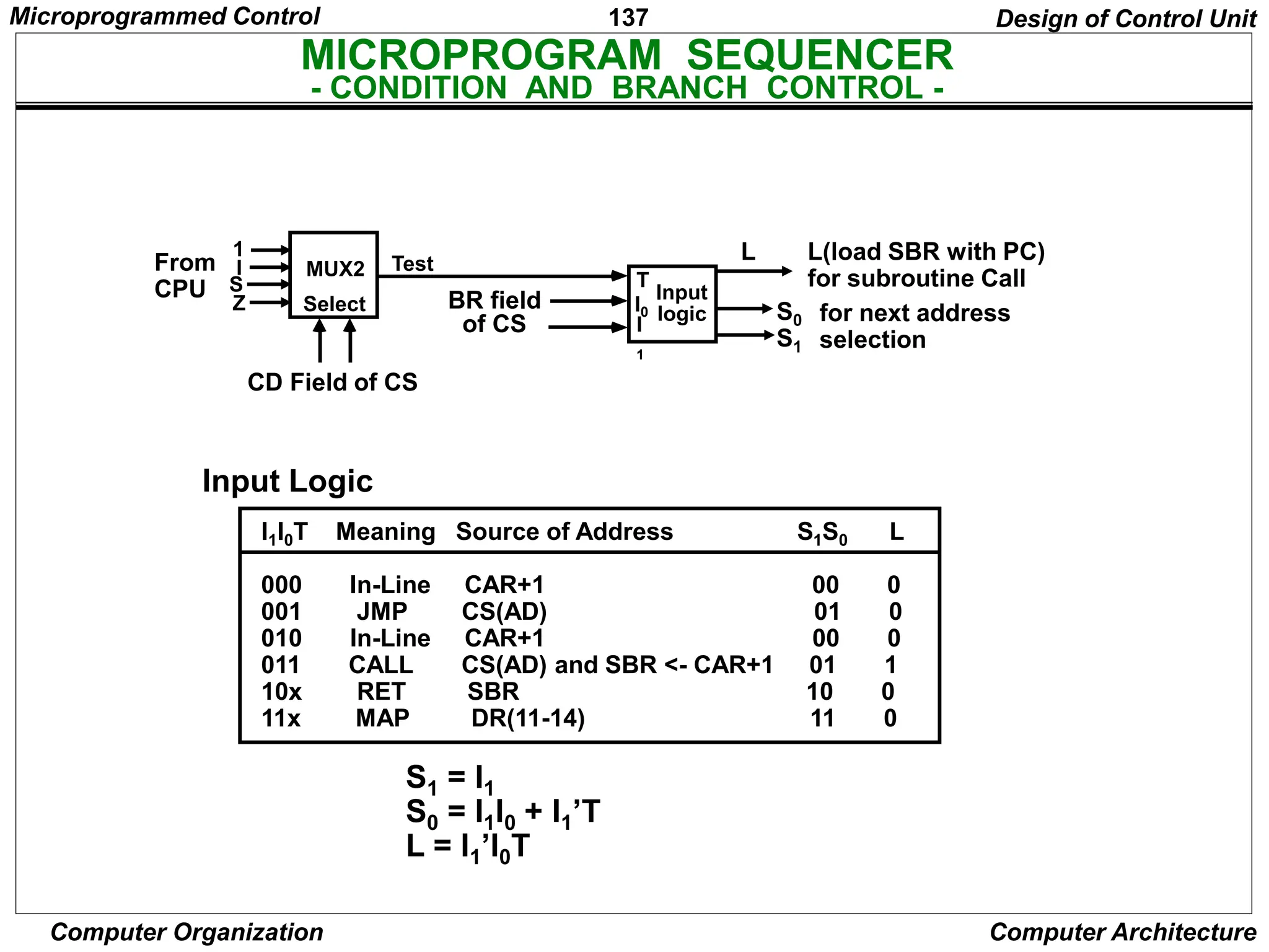
![128
Computer Organization Computer Architecture
MACHINE INSTRUCTION FORMAT
Microinstruction Format
Microprogram
EA is the effective address
Symbol OP-code Description
ADD 0000 AC AC + M[EA]
BRANCH 0001 if (AC < 0) then (PC EA)
STORE 0010 M[EA] AC
EXCHANGE 0011 AC M[EA], M[EA] AC
Machine instruction format
I Opcode
15 14 11 10
Address
0
Sample machine instructions
F1 F2 F3 CD BR AD
3 3 3 2 2 7
F1, F2, F3: Microoperation fields
CD: Condition for branching
BR: Branch field
AD: Address field
Microprogrammed Control](https://image.slidesharecdn.com/computer-system-architecture-morris-mano-220720124304-fefd641d-240725153218-d7339dd3/75/computer-system-architecture-morris-mano-220720124304-fefd641d-ppt-128-2048.jpg)
![129
Computer Organization Computer Architecture
MICROINSTRUCTION FIELD DESCRIPTIONS - F1,F2,F3
F1 Microoperation Symbol
000 None NOP
001 AC AC + DR ADD
010 AC 0 CLRAC
011 AC AC + 1 INCAC
100 AC DR DRTAC
101 AR DR(0-10) DRTAR
110 AR PC PCTAR
111 M[AR] DR WRITE
Microprogram
F2 Microoperation Symbol
000 None NOP
001 AC AC - DR SUB
010 AC AC DR OR
011 AC AC DR AND
100 DR M[AR] READ
101 DR AC ACTDR
110 DR DR + 1 INCDR
111 DR(0-10) PC PCTDR
F3 Microoperation Symbol
000 None NOP
001 AC AC DR XOR
010 AC AC’ COM
011 AC shl AC SHL
100 AC shr AC SHR
101 PC PC + 1 INCPC
110 PC AR ARTPC
111 Reserved
Microprogrammed Control](https://image.slidesharecdn.com/computer-system-architecture-morris-mano-220720124304-fefd641d-240725153218-d7339dd3/75/computer-system-architecture-morris-mano-220720124304-fefd641d-ppt-129-2048.jpg)
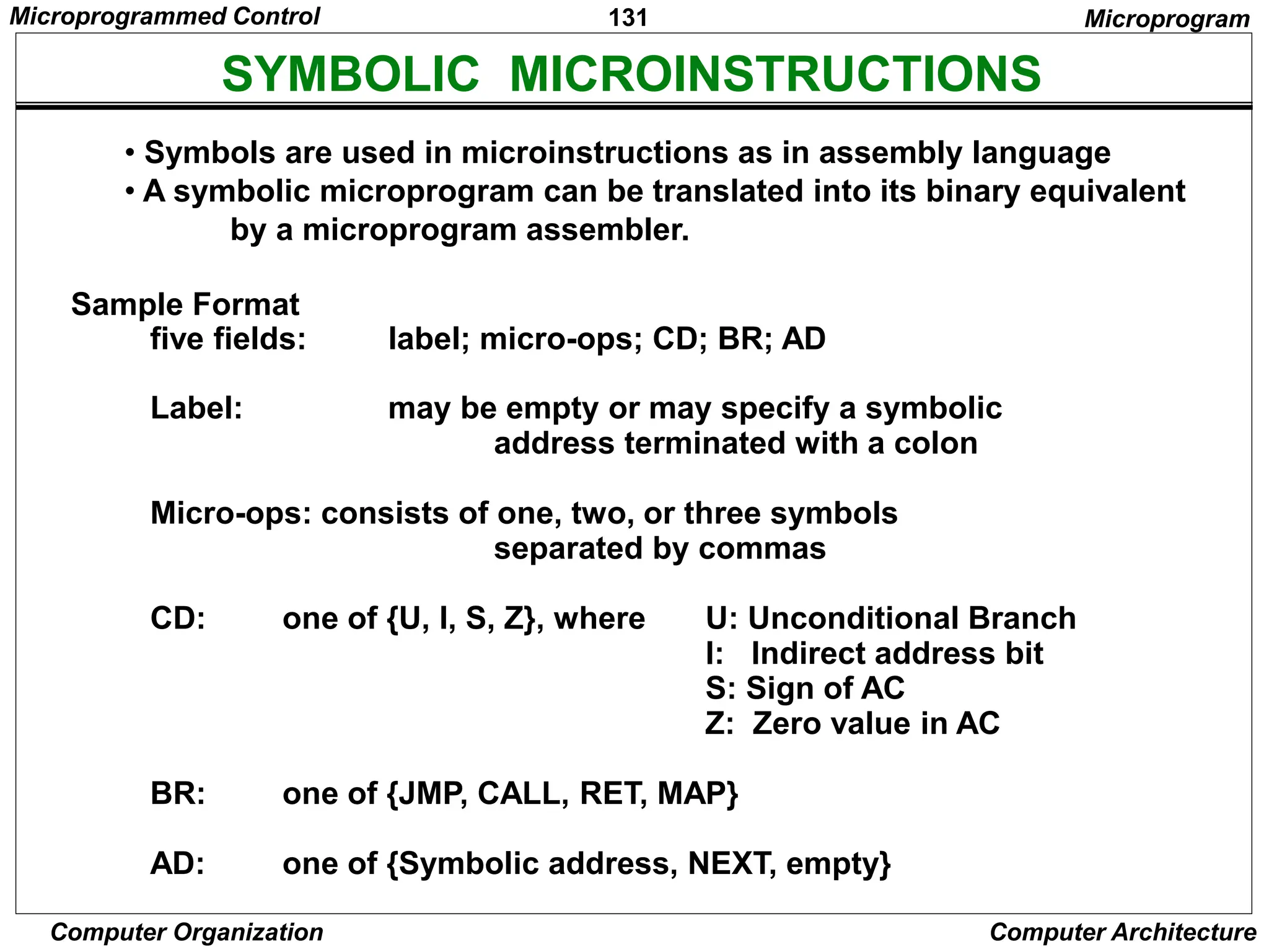
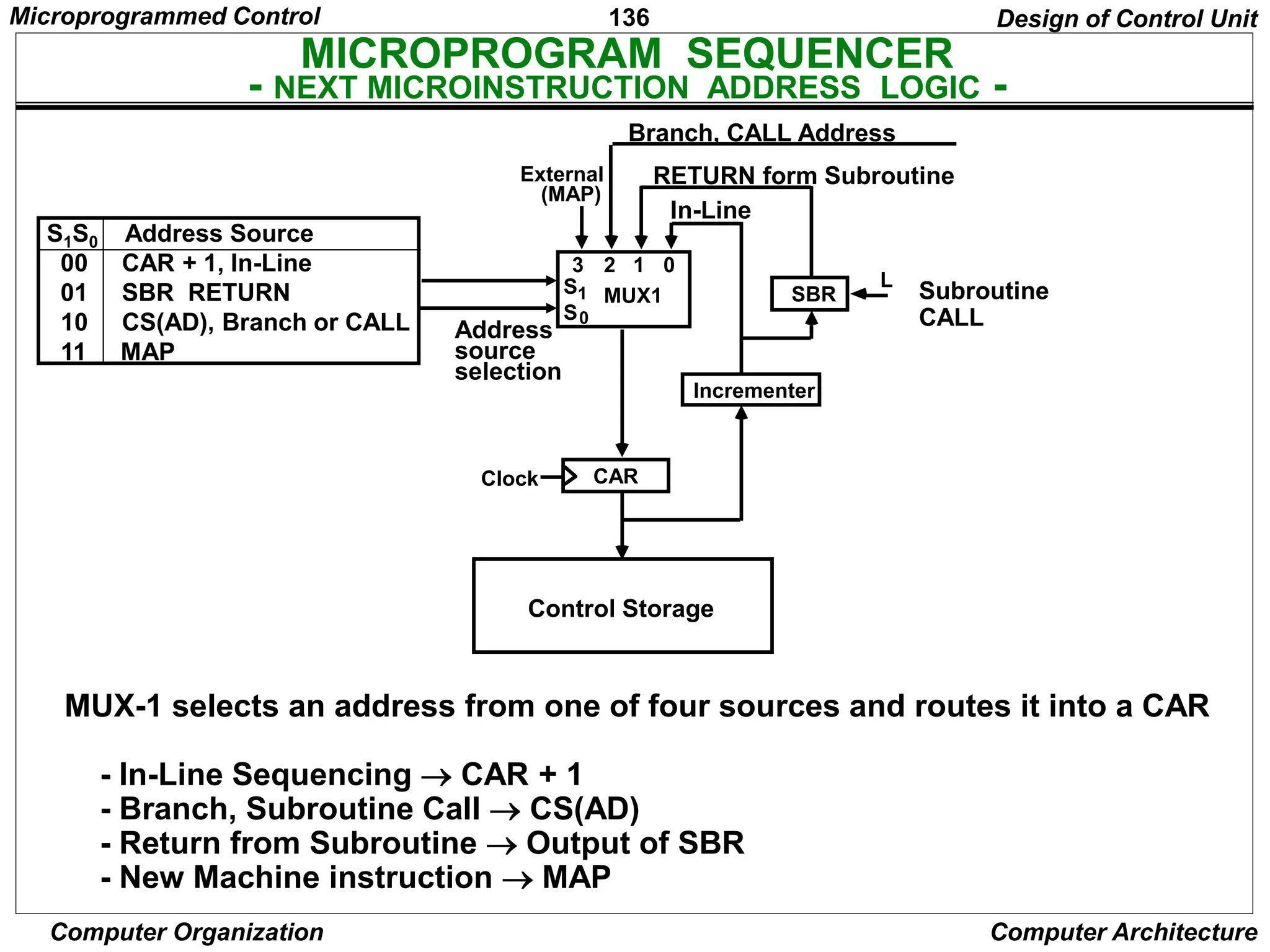
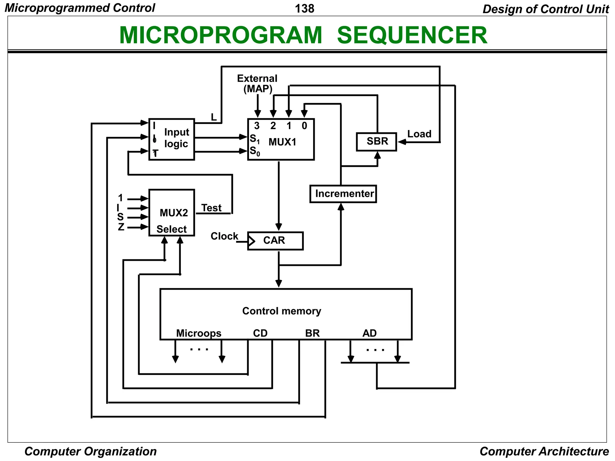
![132
Computer Organization Computer Architecture
SYMBOLIC MICROPROGRAM - FETCH ROUTINE
AR PC
DR M[AR], PC PC + 1
AR DR(0-10), CAR(2-5) DR(11-14), CAR(0,1,6) 0
Symbolic microprogram for the fetch cycle:
ORG 64
PCTAR U JMP NEXT
READ, INCPC U JMP NEXT
DRTAR U MAP
FETCH:
Binary equivalents translated by an assembler
1000000 110 000 000 00 00 1000001
1000001 000 100 101 00 00 1000010
1000010 101 000 000 00 11 0000000
Binary
address F1 F2 F3 CD BR AD
Microprogram
During FETCH, Read an instruction from memory
and decode the instruction and update PC
Sequence of microoperations in the fetch cycle:
Microprogrammed Control](https://image.slidesharecdn.com/computer-system-architecture-morris-mano-220720124304-fefd641d-240725153218-d7339dd3/75/computer-system-architecture-morris-mano-220720124304-fefd641d-ppt-132-2048.jpg)
![145
Computer Organization Computer Architecture
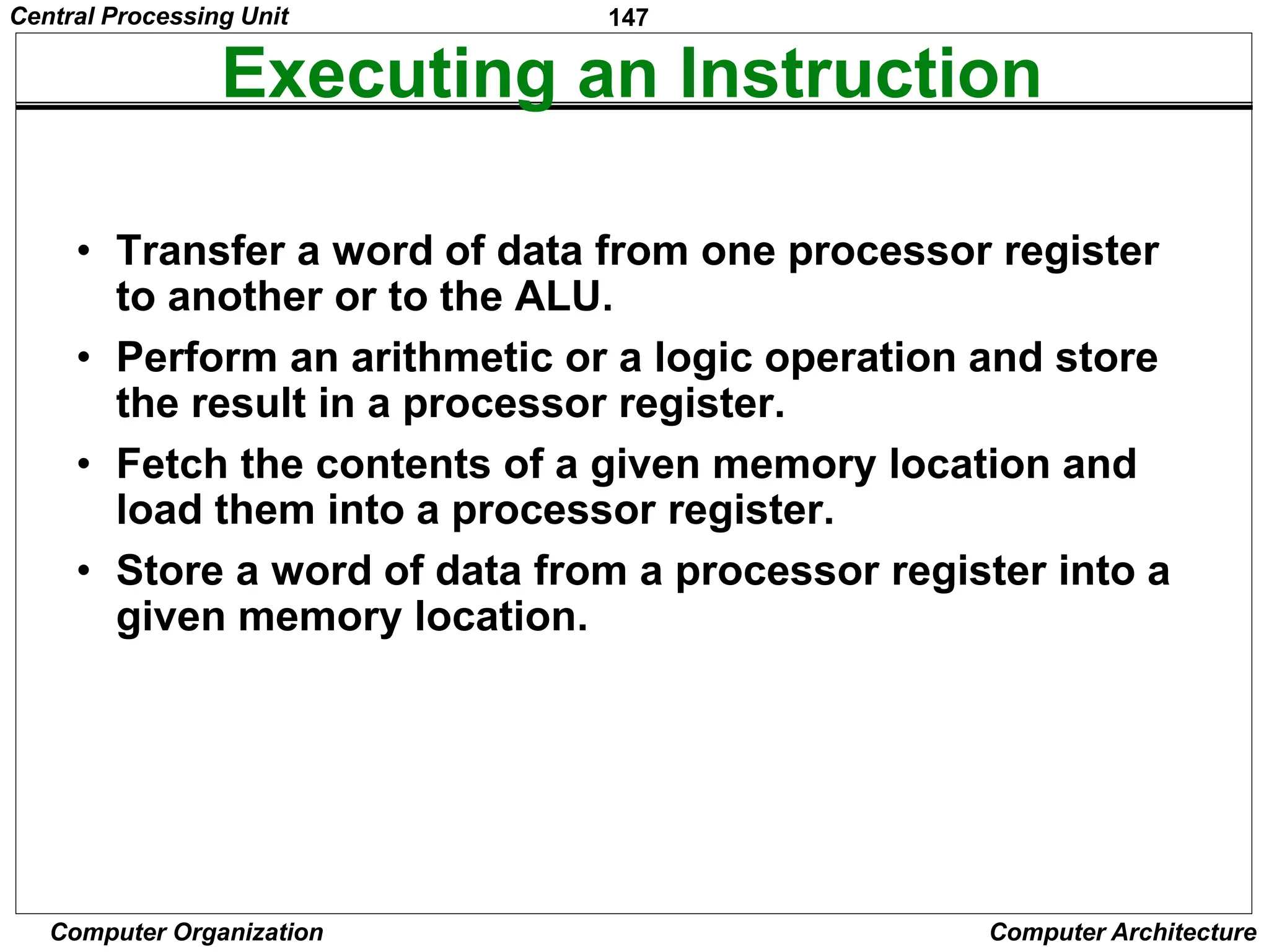
Executing an Instruction
• Fetch the contents of the memory location
pointed to by the PC. The contents of this
location are loaded into the IR (fetch phase).
IR ← [[PC]]
• Assuming that the memory is byte addressable,
increment the contents of the PC by 4 (fetch
phase).
PC ← [PC] + 4
• Carry out the actions specified by the instruction
in the IR (execution phase).
Central Processing Unit](https://image.slidesharecdn.com/computer-system-architecture-morris-mano-220720124304-fefd641d-240725153218-d7339dd3/75/computer-system-architecture-morris-mano-220720124304-fefd641d-ppt-145-2048.jpg)
![152
Computer Organization Computer Architecture
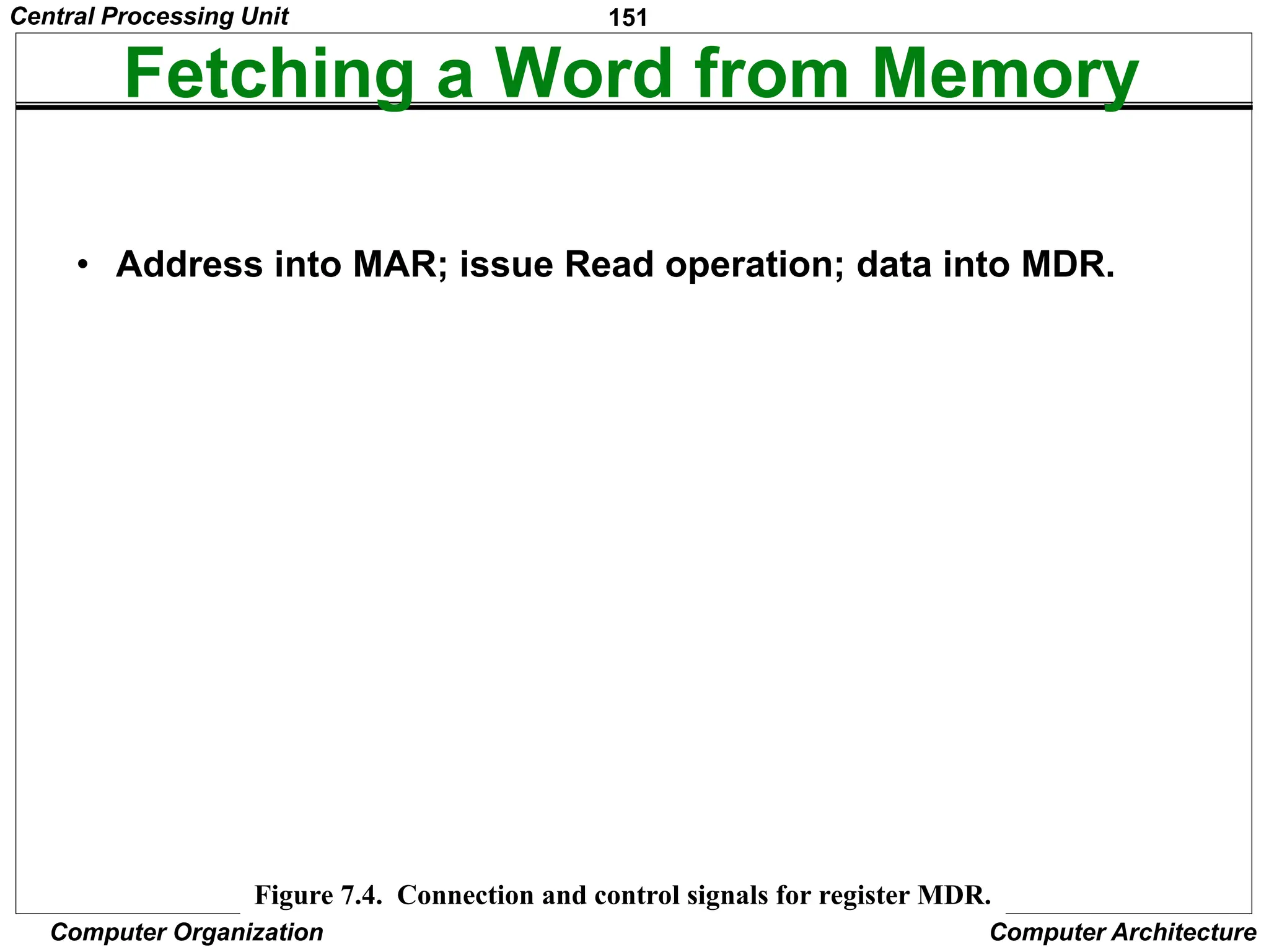
Fetching a Word from Memory
• The response time of each memory access
varies (cache miss, memory-mapped I/O,…).
• To accommodate this, the processor waits until
it receives an indication that the requested
operation has been completed (Memory-
Function-Completed, MFC).
• Move (R1), R2
MAR ← [R1]
Start a Read operation on the memory bus
Wait for the MFC response from the memory
Load MDR from the memory bus
R2 ← [MDR]
Central Processing Unit](https://image.slidesharecdn.com/computer-system-architecture-morris-mano-220720124304-fefd641d-240725153218-d7339dd3/75/computer-system-architecture-morris-mano-220720124304-fefd641d-ppt-152-2048.jpg)
![153
Computer Organization Computer Architecture
Timing
Figure 7.5. Timing of a memory Read operation.
MFC
MDRout
Assume MAR
is always available
on the address lines
of the memory bus.
R2 ← [MDR]
MAR ← [R1]
Start a Read operation on the memory bus
Wait for the MFC response from the memory
Load MDR from the memory bus
Central Processing Unit](https://image.slidesharecdn.com/computer-system-architecture-morris-mano-220720124304-fefd641d-240725153218-d7339dd3/75/computer-system-architecture-morris-mano-220720124304-fefd641d-ppt-153-2048.jpg)
![177
Computer Organization Computer Architecture
OP code 0 1 0 Rsrc Rdst
Mode
Contents of IR
0
3
4
7
8
10
11
Figure 7.21.Microinstruction for Add (Rsrc)+,Rdst.
Note:Microinstruction at location 170 is not executed for this addressing mode.
Address Microinstruction
(octal)
000 PC
out
, MARin, Read, Select
4, Add, Z
in
001 Zout
, PC
in, Yin, WMFC
002 MDRout
, IRin
003 Branch {
PC 101 (from Instruction decoder);
PC
5,4 [IR10,9
]; PC
3
121 Rsrc
out, MAR
in, Read, Select4, Add, Z
in
122 Zout
, Rsrc
in
123
170 MDRout
, MARin, Read, WMFC
171 MDRout
, Yin
172 Rdst
out, SelectY
, Add, Z
in
173 Zout
, Rdst
in, End
[IR10] ×
[IR9] ×
[IR8]}
Branch {
PC 170;PC
0 [IR8]}, WMFC
Microprogrammed Control](https://image.slidesharecdn.com/computer-system-architecture-morris-mano-220720124304-fefd641d-240725153218-d7339dd3/75/computer-system-architecture-morris-mano-220720124304-fefd641d-ppt-177-2048.jpg)

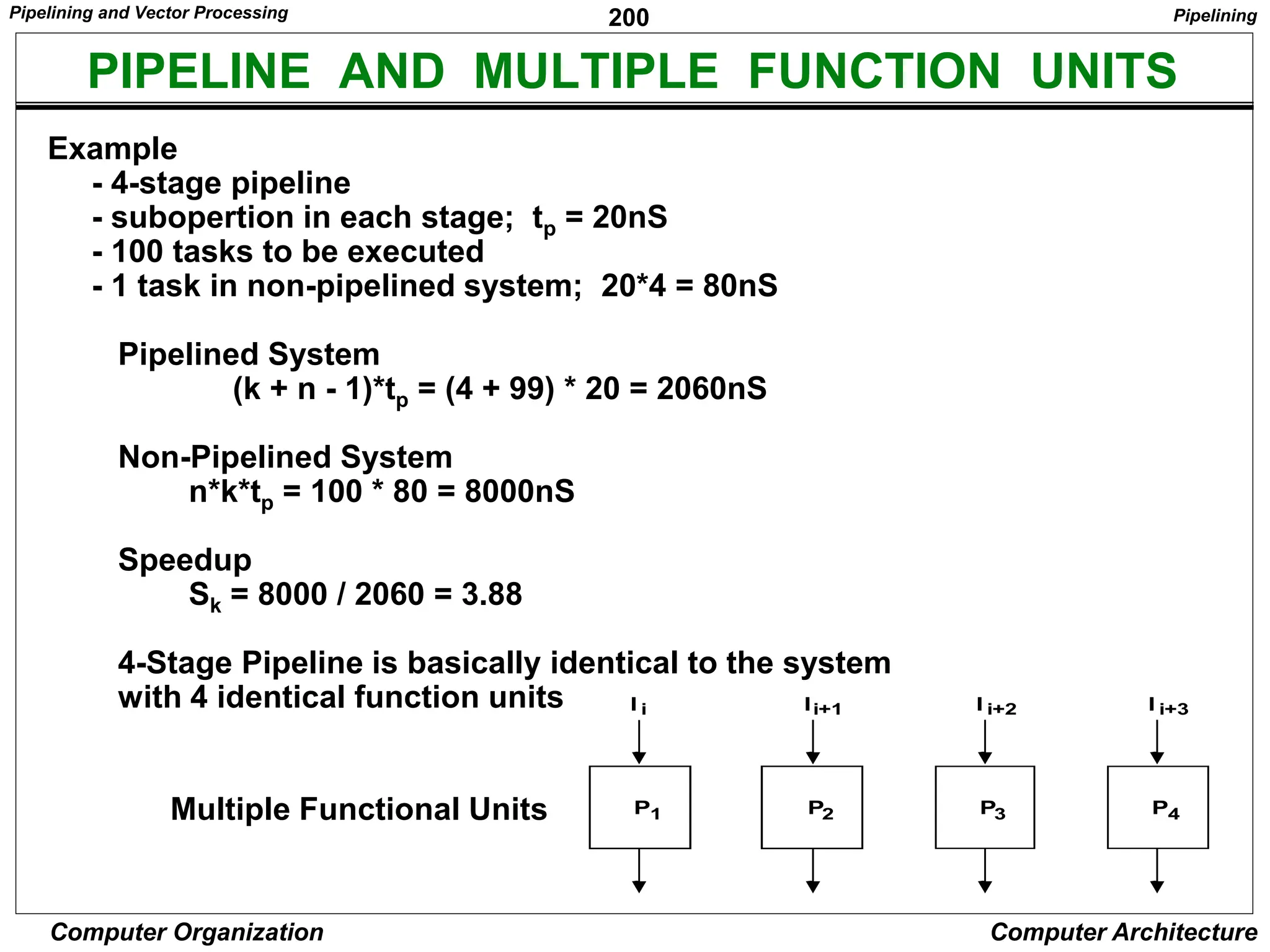
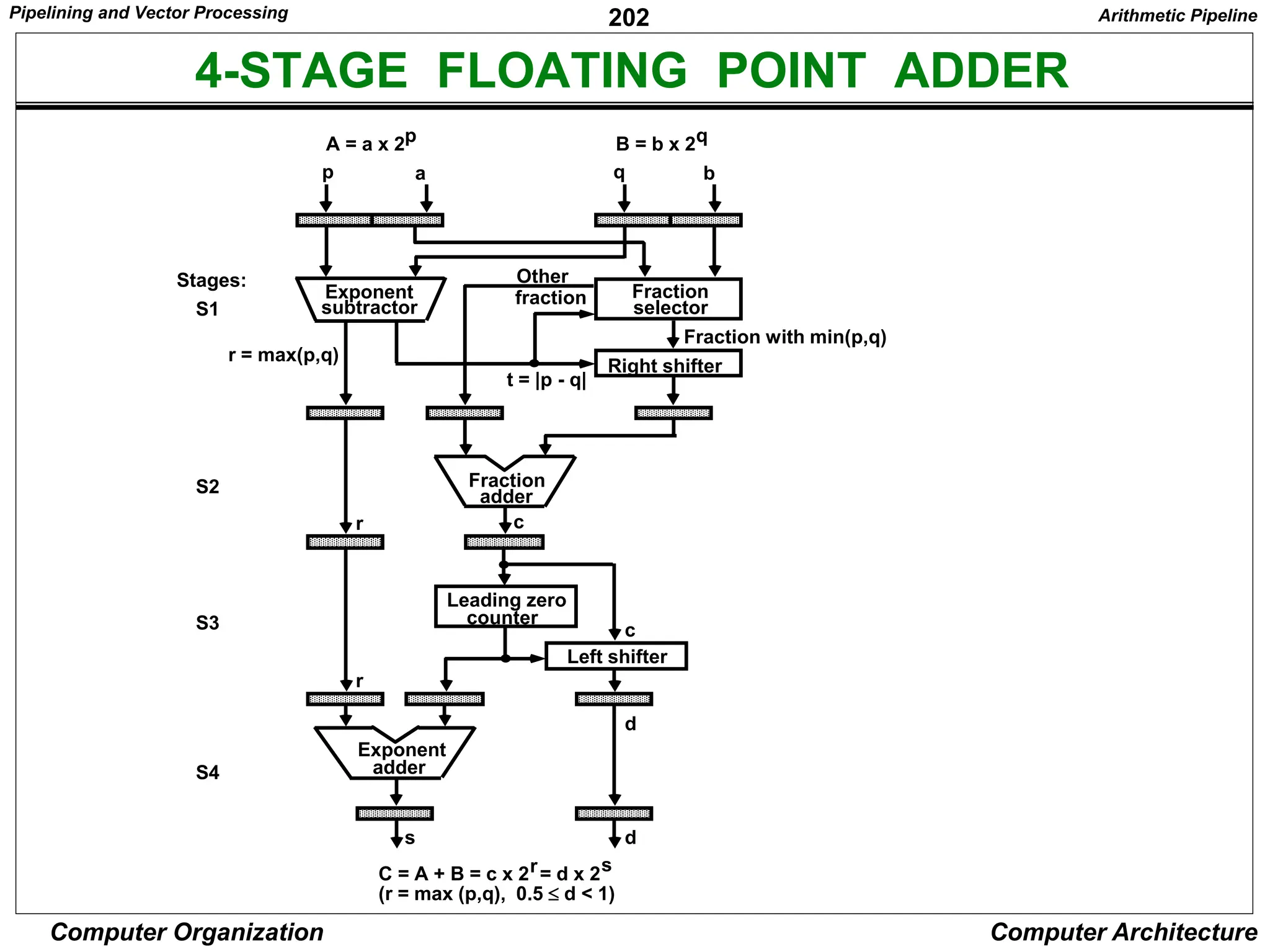
![201
Computer Organization Computer Architecture
ARITHMETIC PIPELINE
Floating-point adder
[1] Compare the exponents
[2] Align the mantissa
[3] Add/sub the mantissa
[4] Normalize the result
X = A x 2a
Y = B x 2b
R
Compare
exponents
by subtraction
a b
R
Choose exponent
Exponents
R
A B
Align mantissa
Mantissas
Difference
R
Add or subtract
mantissas
R
Normalize
result
R
R
Adjust
exponent
R
Segment 1:
Segment 2:
Segment 3:
Segment 4:
Arithmetic Pipeline
Pipelining and Vector Processing](https://image.slidesharecdn.com/computer-system-architecture-morris-mano-220720124304-fefd641d-240725153218-d7339dd3/75/computer-system-architecture-morris-mano-220720124304-fefd641d-ppt-201-2048.jpg)
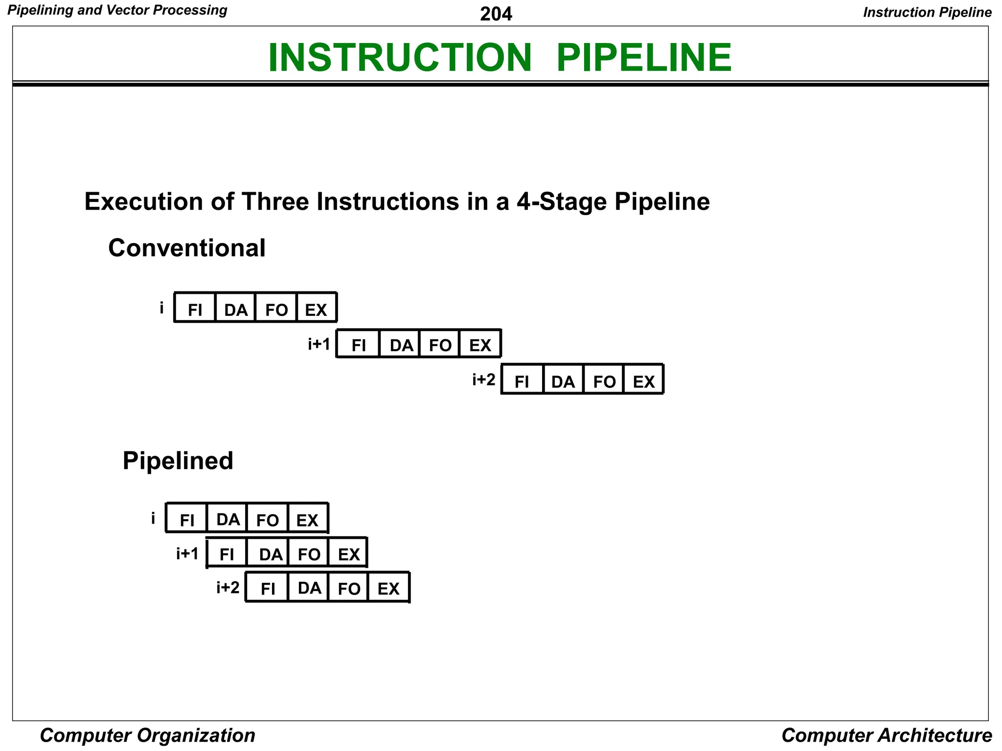
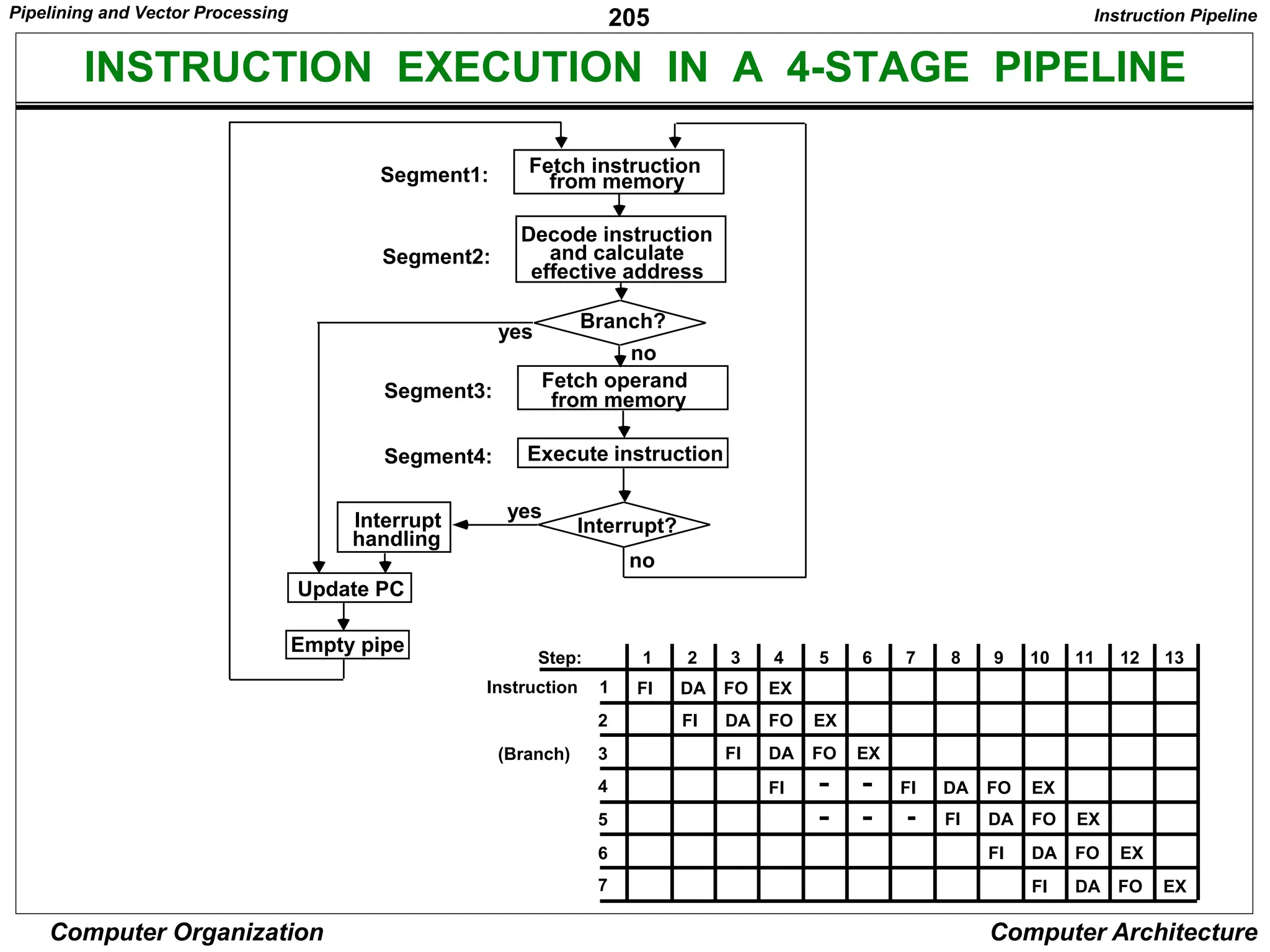
![203
Computer Organization Computer Architecture
INSTRUCTION CYCLE
Six Phases* in an Instruction Cycle
[1] Fetch an instruction from memory
[2] Decode the instruction
[3] Calculate the effective address of the operand
[4] Fetch the operands from memory
[5] Execute the operation
[6] Store the result in the proper place
* Some instructions skip some phases
* Effective address calculation can be done in
the part of the decoding phase
* Storage of the operation result into a register
is done automatically in the execution phase
==> 4-Stage Pipeline
[1] FI: Fetch an instruction from memory
[2] DA: Decode the instruction and calculate
the effective address of the operand
[3] FO: Fetch the operand
[4] EX: Execute the operation
Instruction Pipeline
Pipelining and Vector Processing](https://image.slidesharecdn.com/computer-system-architecture-morris-mano-220720124304-fefd641d-240725153218-d7339dd3/75/computer-system-architecture-morris-mano-220720124304-fefd641d-ppt-203-2048.jpg)
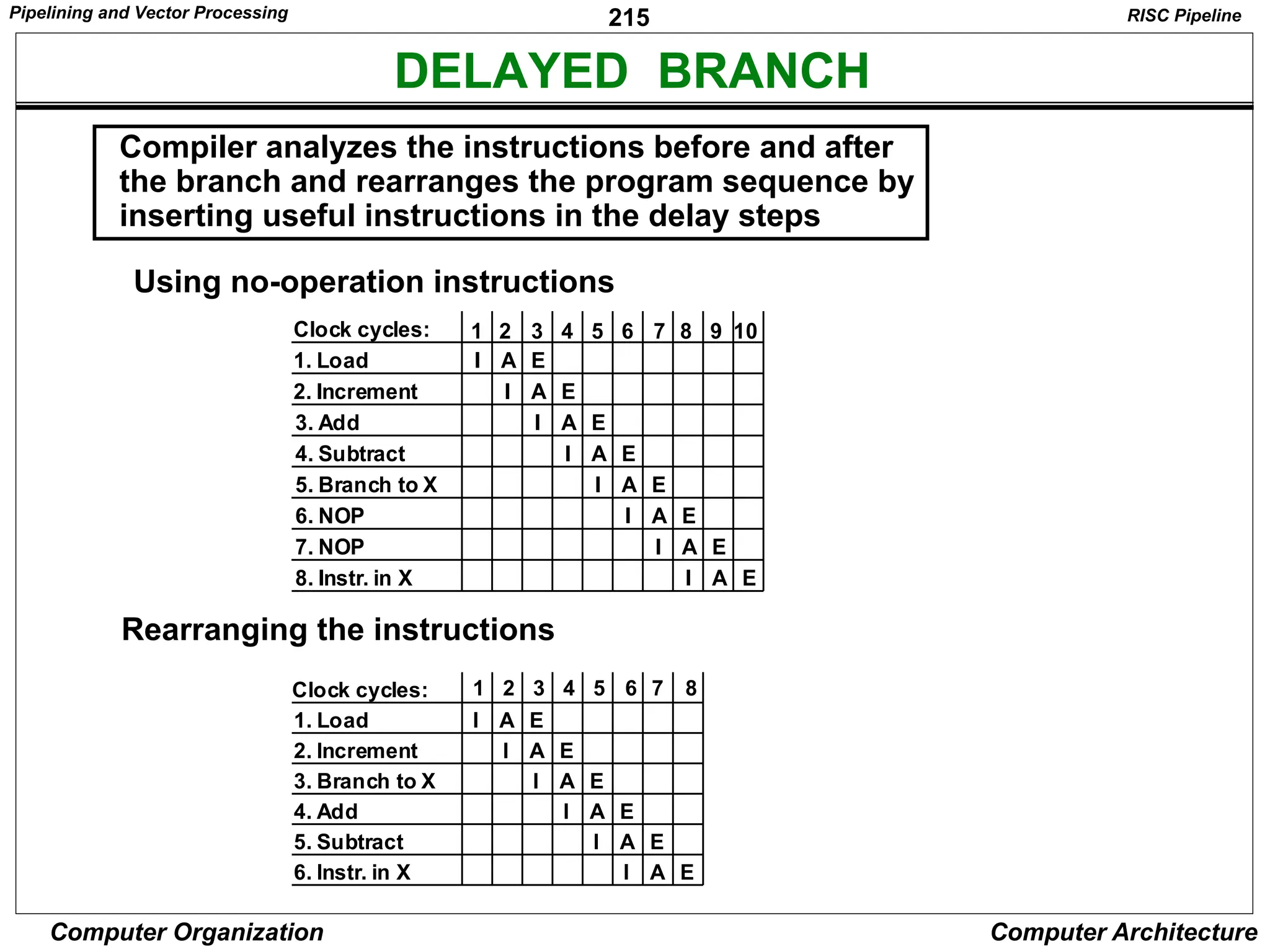
![214
Computer Organization Computer Architecture
DELAYED LOAD
Three-segment pipeline timing
Pipeline timing with data conflict
clock cycle 1 2 3 4 5 6
Load R1 I A E
Load R2 I A E
Add R1+R2 I A E
Store R3 I A E
Pipeline timing with delayed load
clock cycle 1 2 3 4 5 6 7
Load R1 I A E
Load R2 I A E
NOP I A E
Add R1+R2 I A E
Store R3 I A E
LOAD: R1 M[address 1]
LOAD: R2 M[address 2]
ADD: R3 R1 + R2
STORE: M[address 3] R3
RISC Pipeline
The data dependency is taken
care by the compiler rather
than the hardware
Pipelining and Vector Processing](https://image.slidesharecdn.com/computer-system-architecture-morris-mano-220720124304-fefd641d-240725153218-d7339dd3/75/computer-system-architecture-morris-mano-220720124304-fefd641d-ppt-214-2048.jpg)
![224
Computer Organization Computer Architecture
SPEEDUP AND EFFICIENCY
A: Given problem
T*(n): Time of best sequential algorithm to solve an
instance of A of size n on 1 processor
Tp(n): Time needed by a given parallel algorithm
and given parallel architecture to solve an
instance of A of size n, using p processors
Note: T*(n) T1(n)
Speedup: T*(n) / Tp(n)
Efficiency: T*(n) / [pTp(n)]
Speedup should be between 0 and p, and
Efficiency should be between 0 and 1
Speedup is linear if there is a constant c > 0
so that speedup is always at least cp.
1 2 3 4 5 6 7 8 9 10
Processors
Speedup
Perfect Speedup
Characteristics of Multiprocessors
Multiprocessors](https://image.slidesharecdn.com/computer-system-architecture-morris-mano-220720124304-fefd641d-240725153218-d7339dd3/75/computer-system-architecture-morris-mano-220720124304-fefd641d-ppt-224-2048.jpg)
![226
Computer Organization Computer Architecture
FLYNN’s HARDWARE TAXONOMY
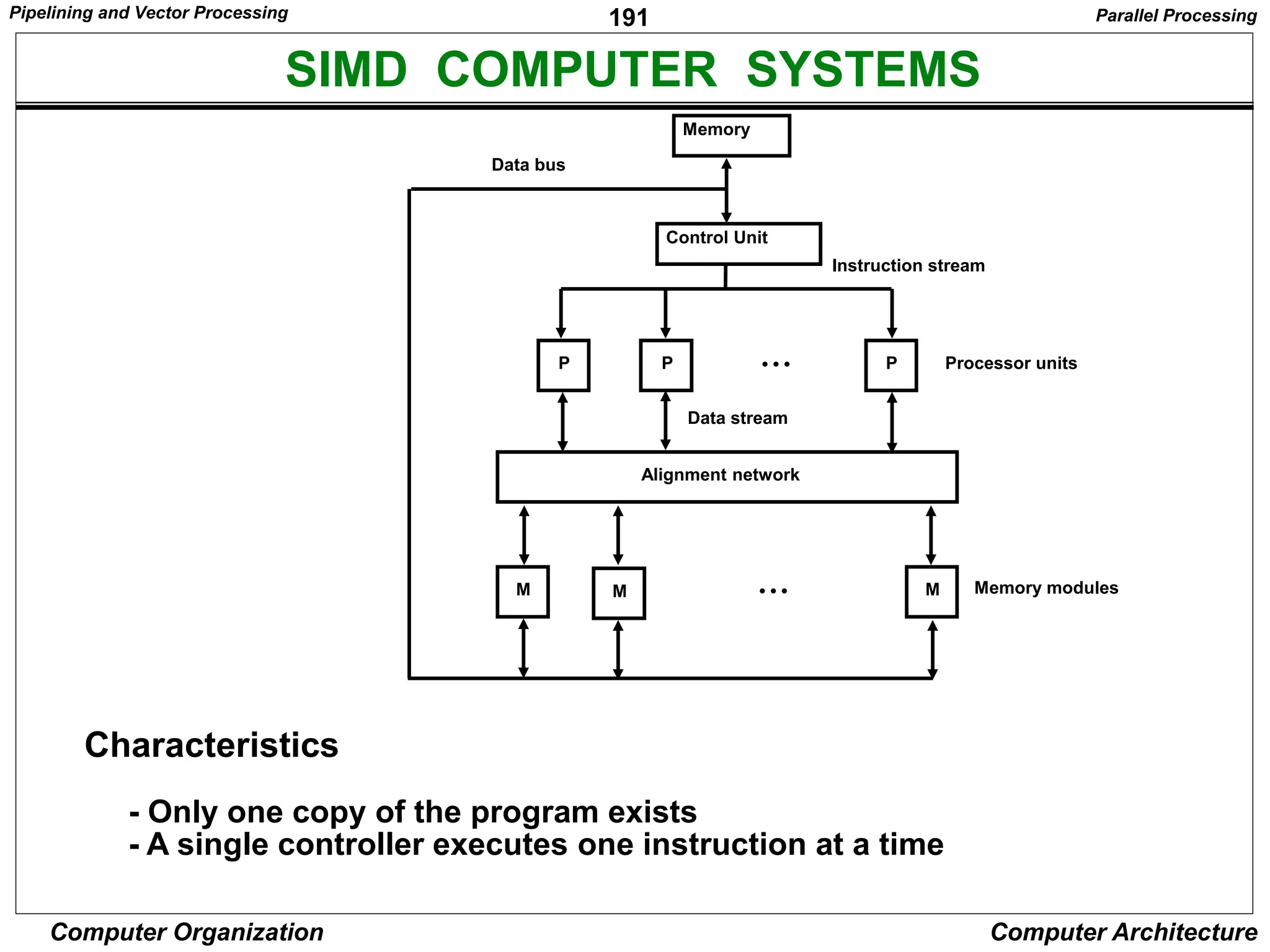
SI: Single Instruction Stream
- All processors are executing the same instruction in the same cycle
- Instruction may be conditional
- For Multiple processors, the control processor issues an instruction
MI: Multiple Instruction Stream
- Different processors may be simultaneously
executing different instructions
SD: Single Data Stream
- All of the processors are operating on the same
data items at any given time
MD: Multiple Data Stream
- Different processors may be simultaneously
operating on different data items
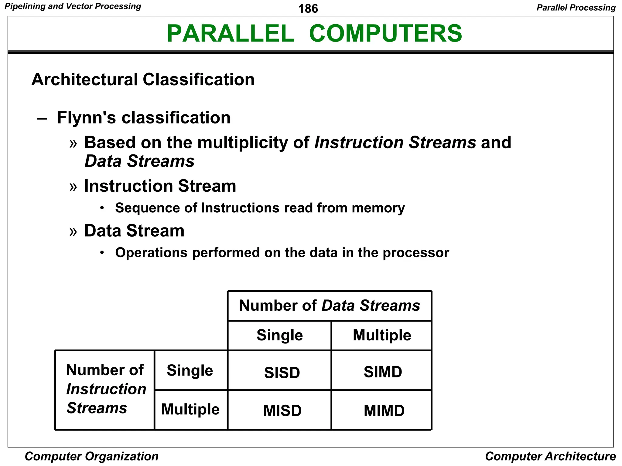
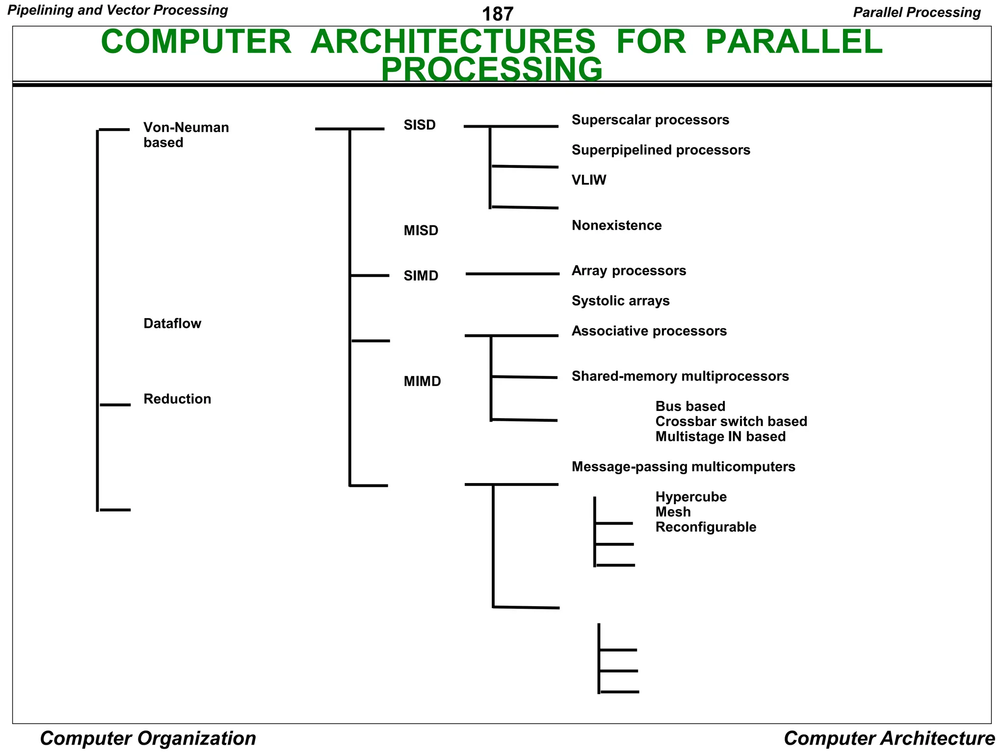
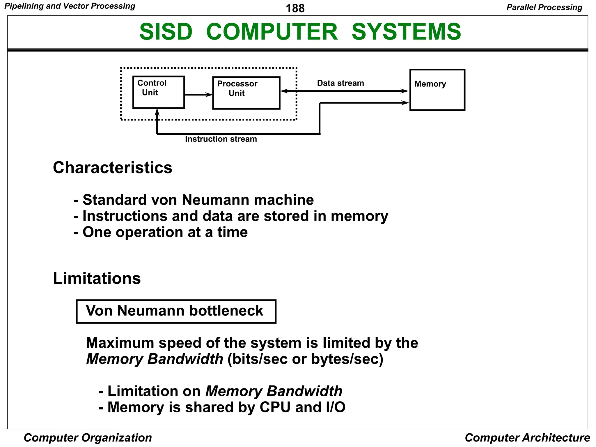
SISD : standard serial computer
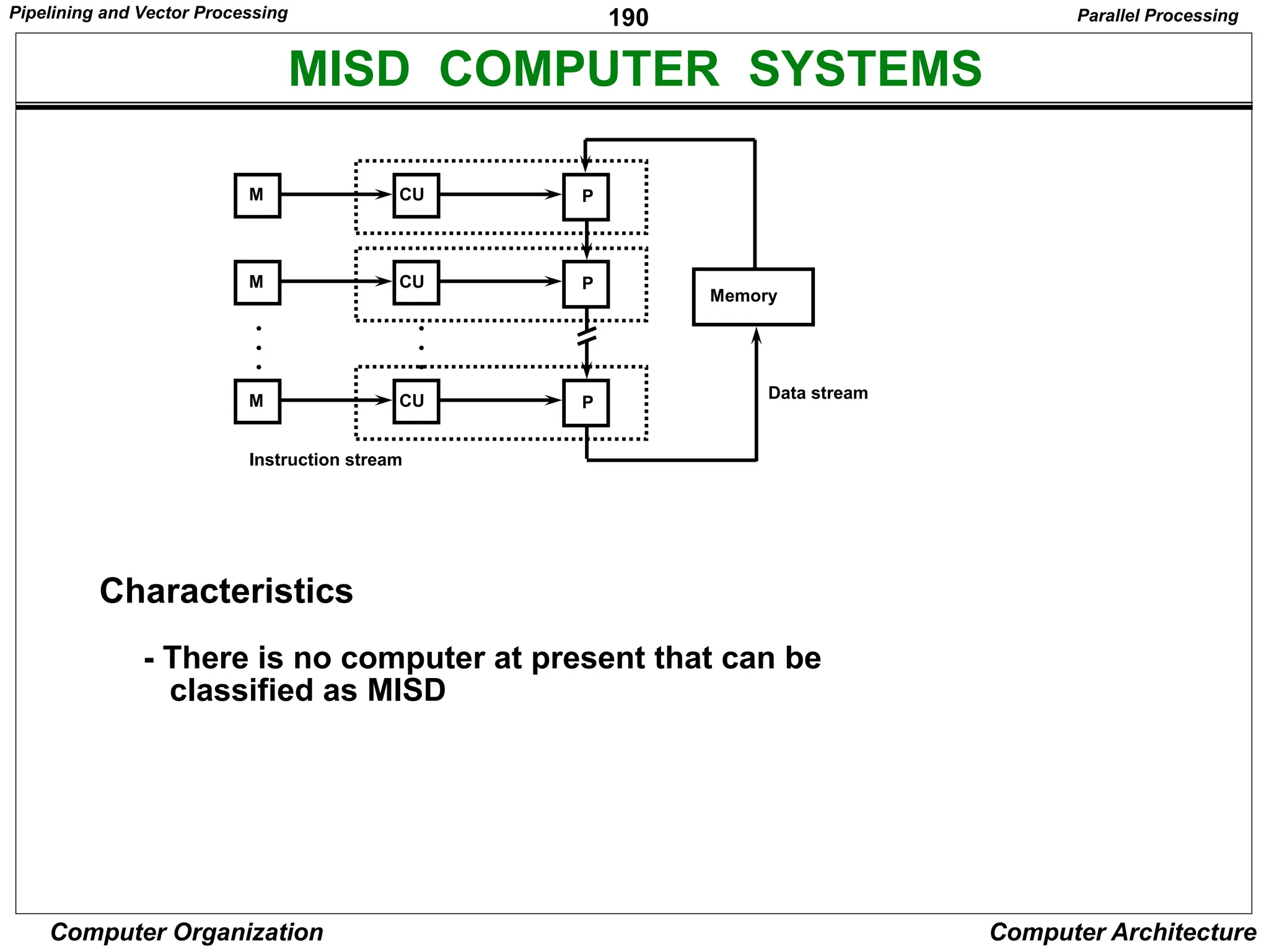
MISD : very rare
MIMD and SIMD : Parallel processing computers
I: Instruction Stream
D: Data Stream
M
S S
[ ] I [ ] D
M
Characteristics of Multiprocessors
Multiprocessors](https://image.slidesharecdn.com/computer-system-architecture-morris-mano-220720124304-fefd641d-240725153218-d7339dd3/75/computer-system-architecture-morris-mano-220720124304-fefd641d-ppt-226-2048.jpg)
![233
Computer Organization Computer Architecture
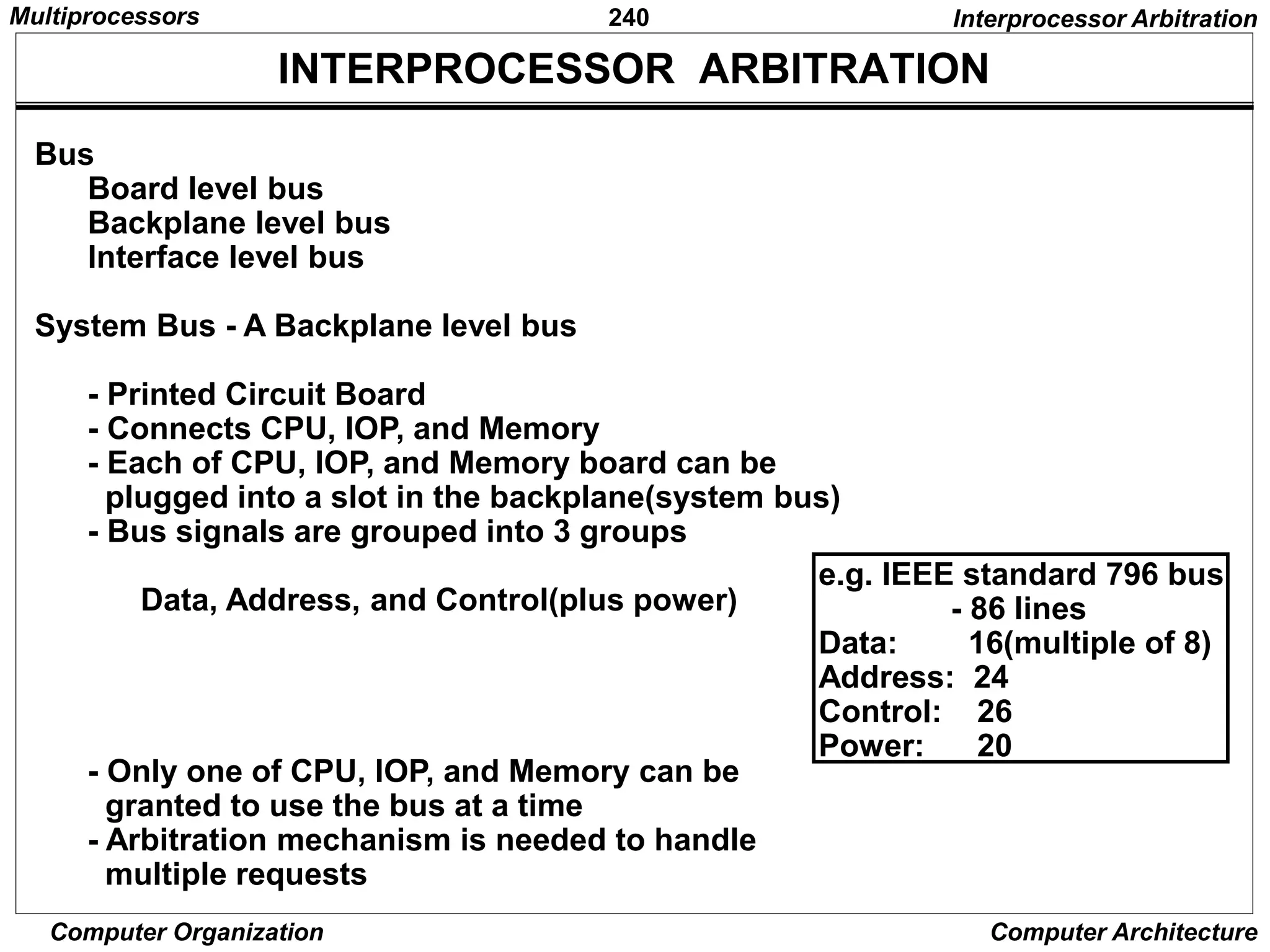
- A collection of signal lines that carry module-to-module communication
- Data highways connecting several digital system elements
Operations of Bus
Bus
M3 wishes to communicate with S5
[1] M3 sends signals (address) on the bus that causes
S5 to respond
[2] M3 sends data to S5 or S5 sends data to
M3(determined by the command line)
Master Device: Device that initiates and controls the communication
Slave Device: Responding device
Multiple-master buses
-> Bus conflict
-> need bus arbitration
Devices
M3 S7 M6 S5 M4
S2
BUS
Interconnection Structure
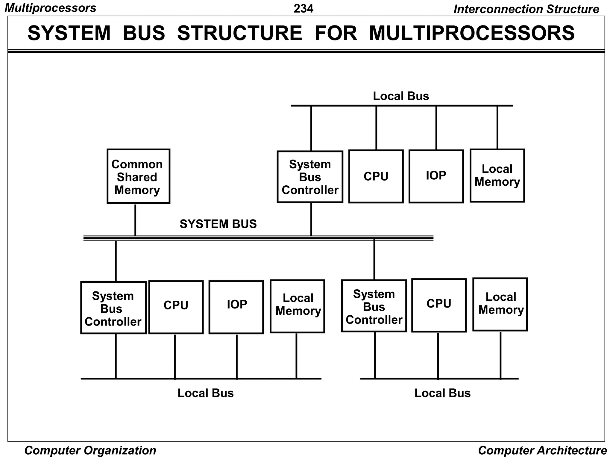
Multiprocessors](https://image.slidesharecdn.com/computer-system-architecture-morris-mano-220720124304-fefd641d-240725153218-d7339dd3/75/computer-system-architecture-morris-mano-220720124304-fefd641d-ppt-233-2048.jpg)
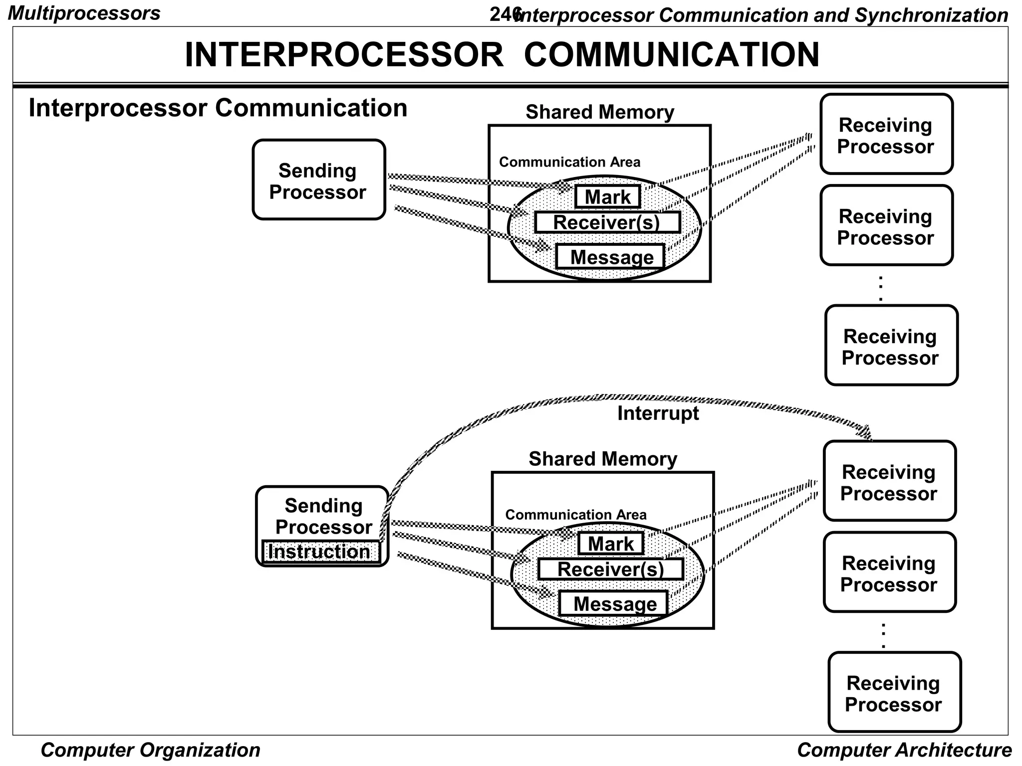
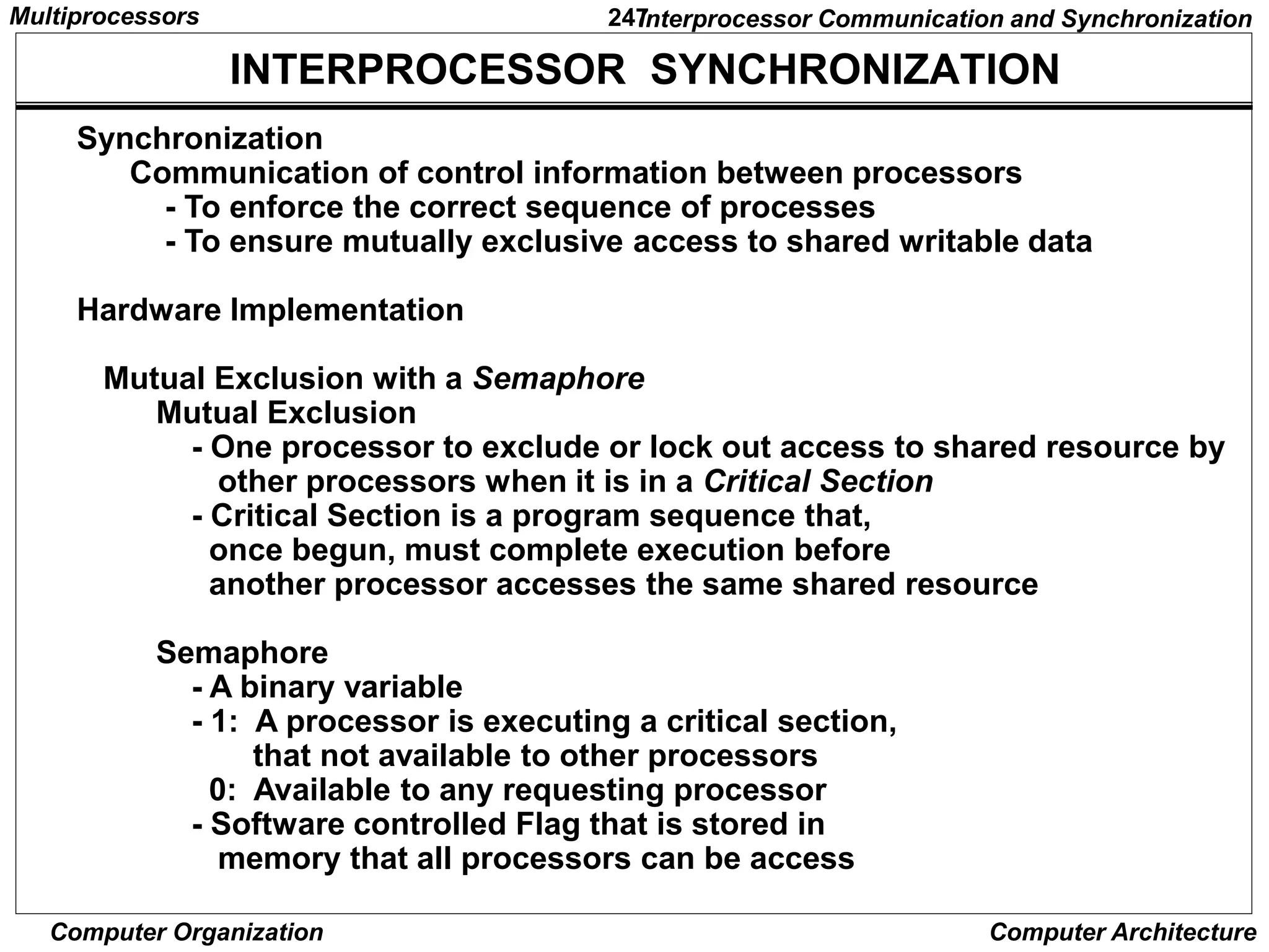
![248
Computer Organization Computer Architecture
SEMAPHORE
Testing and Setting the Semaphore
- Avoid two or more processors test or set the same semaphore
- May cause two or more processors enter the
same critical section at the same time
- Must be implemented with an indivisible operation
R <- M[SEM] / Test semaphore /
M[SEM] <- 1 / Set semaphore /
These are being done while locked, so that other processors cannot test
and set while current processor is being executing these instructions
If R=1, another processor is executing the
critical section, the processor executed
this instruction does not access the
shared memory
If R=0, available for access, set the semaphore to 1 and access
The last instruction in the program must clear the semaphore
Interprocessor Communication and Synchronization
Multiprocessors](https://image.slidesharecdn.com/computer-system-architecture-morris-mano-220720124304-fefd641d-240725153218-d7339dd3/75/computer-system-architecture-morris-mano-220720124304-fefd641d-ppt-248-2048.jpg)
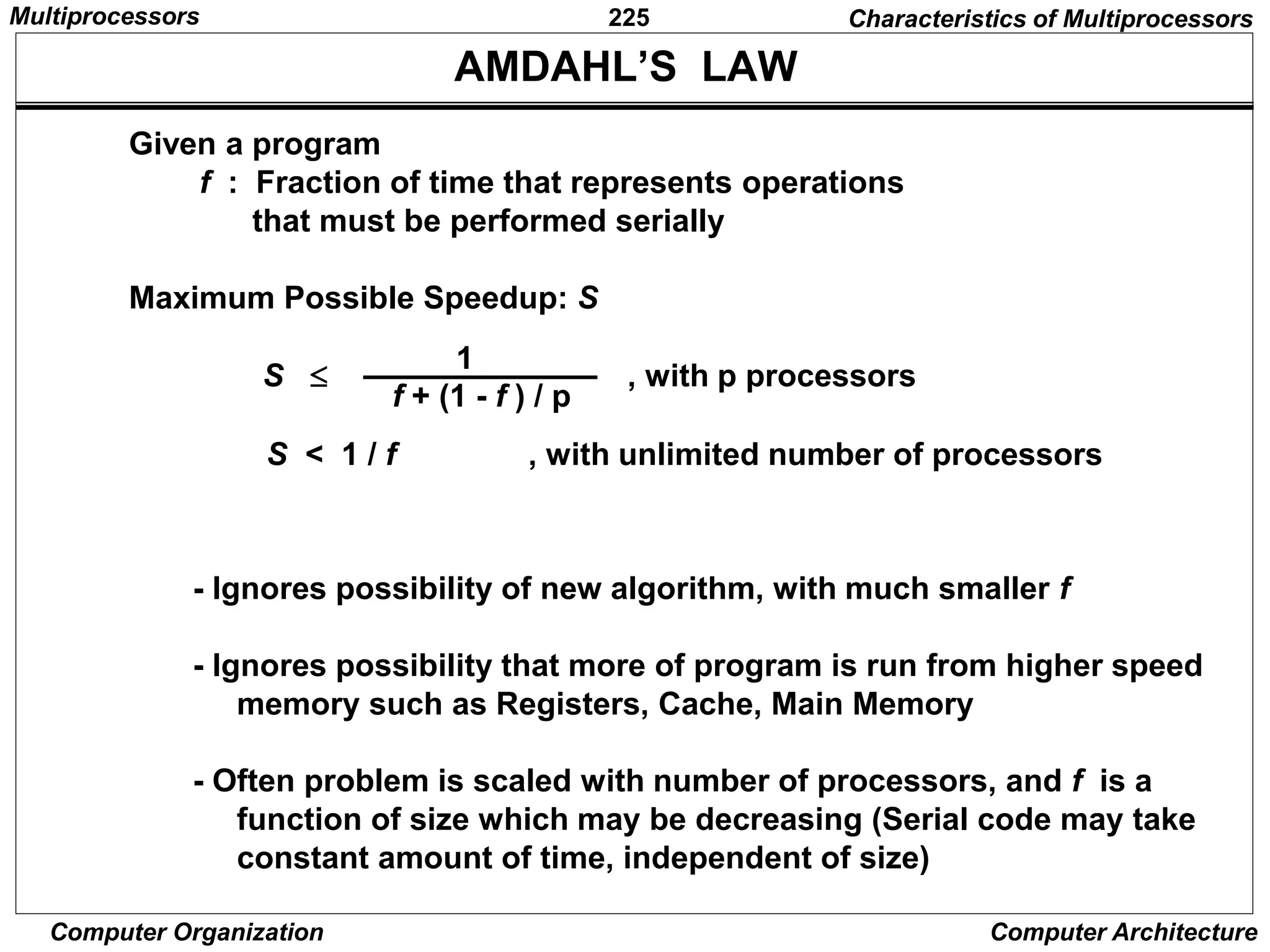
![252
Computer Organization Computer Architecture
PARALLEL COMPUTING
n
Amdahl’s Law
A small number of sequential operations can effectively
limit the speedup of a parallel algorithm.
Let f be the fraction of operations in a computation that must be performed sequentially,
where 0 < f < 1. Then the maximum speedup S achievable by a parallel computer with p processors
performing the computation is S < 1 / [f + (1 - f) / p]. For example, if 10% of the computation must be
performed sequentially, then the maximum speedup achievable is 10, no matter how many
processors a parallel computer has.
There exist some parallel algorithms with almost no sequential operations. As the problem size(n)
increases, f becomes smaller (f -> 0 as n->In this case, lim S = p.
Parallel Computing
History
History tells us that the speed of traditional single CPU
Computers has increased 10 folds every 5 years.
Why should great effort be expended to devise a parallel
computer that will perform tasks 10 times faster when,
by the time the new architecture is developed and
implemented, single CPU computers will be just as fast.
Utilizing parallelism is better than waiting.
Multiprocessors](https://image.slidesharecdn.com/computer-system-architecture-morris-mano-220720124304-fefd641d-240725153218-d7339dd3/75/computer-system-architecture-morris-mano-220720124304-fefd641d-ppt-252-2048.jpg)
![260
Computer Organization Computer Architecture
MIN SPACE
• Baseline [Wu80]
• Flip [Batcher76]
• Indirect binary
n-cube [Peas77]
• Omega [Lawrie75]
• Regular SW banyan
[Goke73]
Delta network [Patel81]
Banyan network
=(unique path network)
PM2I network
• Data Manipulator
[Feng74]
• Augmented DM
[Siegel78]
• Inverse ADM
[Siegel79]
• Gamma [Parker84]
• Extra stage Cube
[Adams82]
• Replicated/Dialted
Delta netork
[Kruskal83]
• B-delta [Yoon88]
Multiple Path Network
Permutation/Sorting Network
( N ! )
• Clos network [53]
• Benes network [62]
• Batcher sorting
network [68]
M I N
Interconnection Structure
Multiprocessors](https://image.slidesharecdn.com/computer-system-architecture-morris-mano-220720124304-fefd641d-240725153218-d7339dd3/75/computer-system-architecture-morris-mano-220720124304-fefd641d-ppt-260-2048.jpg)