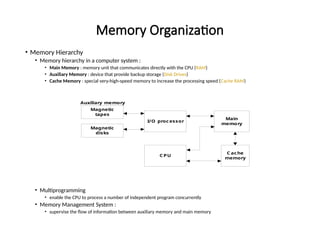
Memory Organization
• MemoryHierarchy
• Memory hierarchy in a computer system :
• Main Memory : memory unit that communicates directly with the CPU (RAM)
• Auxiliary Memory : device that provide backup storage (Disk Drives)
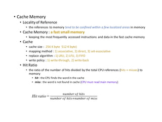
• Cache Memory : special very-high-speed memory to increase the processing speed (Cache RAM)
• Multiprogramming
• enable the CPU to process a number of independent program concurrently
• Memory Management System :
• supervise the flow of information between auxiliary memory and main memory
Magnetic
tapes
Magnetic
disks
I/O proc essor
C PU
Main
memory
C ache
memory
Auxiliary memory
2.
Main Memory
Theprincipal technology used for the main memory is based on semiconductor
integrated circuits such as RAM and ROM chips.
RAM chips are available in two possible operating modes, static and dynamic.
The static RAM consists of internal flip-flops that store the binary information. The
stored information remains valid as long as power is applied to the unit.
The dynamic RAM stores the binary information in the form of electric charges
that are applied to capacitors.The dynamic RAM offers reduced power
consumption and larger storage capacity in a single memory chip. The static RAM
is easier to use and has shorter read and write cycles.
Most of the main memory in a general-purpose computer is made up of RAM
integrated circuit chips, but a portion of the memory may be constructed with ROM
chips.
04/08/2025
3.
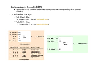
Bootstrap Loader (storedin ROM)
• A program whose function is to start the computer software operating when power is
turned on
• RAM and ROM Chips
• Typical RAM chip :
• 128 X 8 RAM : 27 = 128 (7 bit address lines)
• Typical ROM chip :
• 512 X 8 ROM : 29
= 512 (9 bit address lines)
×
128× 8
RAM
CS1
AD7
WR
RD
CS2
Chip select 1
Chip select 2
Read
Write
7 bit address
8 bit data bus
(a) Block diagram
CS1 WR
RD
CS2 Memory function State of data bus
0
×
×
×
0
0 0
0 0
0
1 1
1
1
1
1
×
0
×
×
0
1
1
Inhibit
Inhibit
Inhibit
Write
Read
Inhibit
High- impedance
High- impedance
High- impedance
Input data to RAM
Output data from RAM
High- impedance
(b) Function table
512× 8
ROM
CS1
AD9
CS2
Chip select 1
Chip select 2
9 bit address
8 bit data bus
4.
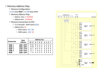
• Memory AddressMap
• Memory Configuration :
1 x 512 byte ROM + 4 x 128 bytes RAM
• Memory Address Map :
• Address lines 9 8 (RAM)
• Address line 10 (ROM)
• Memory Connection to CPU :
• 2 x 4 Decoder : RAM select (CS1)
• Address line 10
• RAM select : CS1 (0)
• ROM select : CS2 (1)
128× 8
RAM 1
C S 1
AD7
WR
RD
C S 2
128× 8
RAM 2
C S 1
AD7
WR
RD
C S 2
128× 8
RAM 4
C S 1
AD7
WR
RD
C S 2
128× 8
RAM 3
C S 1
AD7
WR
RD
C S 2
128× 8
ROM
C S 1
C S 2
AD9
Data
Data
Data
Data
Data
C PU
WR
RD
16 - 11 10 9 8 7 - 1
Address bus
Data bus
Dec oder
3 2 1 0
1- 7
8
9
5.
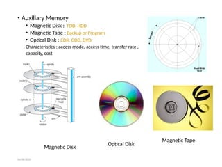
• Auxiliary Memory
•Magnetic Disk : FDD, HDD
• Magnetic Tape : Backup or Program
• Optical Disk : CDR, ODD, DVD
Characteristics : access mode, access time, transfer rate ,
capacity, cost
04/08/2025
Magnetic Disk
Optical Disk
Magnetic Tape
text
text
text
text
S
e
c
t
o
r
Read/Write
head
Tracks
6.
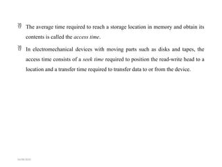
The averagetime required to reach a storage location in memory and obtain its
contents is called the access time.
In electromechanical devices with moving parts such as disks and tapes, the
access time consists of a seek time required to position the read-write head to a
location and a transfer time required to transfer data to or from the device.
04/08/2025
7.
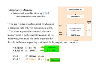
• Associative Memory
•Content Addressable Memory (CAM)
• A memory unit accessed by content
• The key register provides a mask for choosing
a particular field or key in the argument word.
• The entire argument is compared with each
memory word if the key register contains all l’s.
Otherwise, only those bits in the argument that
have l's in their corresponding position of the key register are compared.
A Register 101 111100
K Register 111 000000
Word 1 100 111100 M = 0
Word 2 101 000011 M = 1
Argument register (A)
Key register (K)
Associative memory
array and logic
m words
n bits per word
M
Match
register
Input
Write
Read
Output
Argument
Key (Mask)
Match Logic
8.
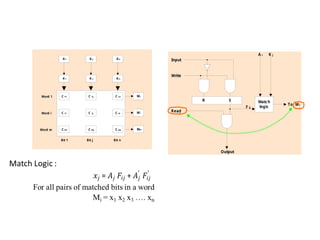
•
A1
C 11
An
A j
K1 K n
K j
C 1j C 1n
C i1 C ij C in
C m1 C mj C mn
M1
Mm
Mi
Bit 1 Bit n
Bit j
Word 1
Word m
Word i
R S Match
logic
Input
Read
Write
Output
To Mi
K j
A i
F ij
9.
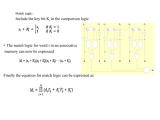
Match Logic :
Includethe key bit Kj in the comparison logic
• The match logic for word i in an associative
memory can now be expressed
Finally the equation for match logic can be expressed as
F'i1 F i1
A 1
K 1
F'i2 F i2
A 2
K 2
F'in Fin
A n
K n
Mi
10.
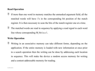
Read Operation
Ifmore than one word in memory matches the unmasked argument field, all the
matched words will have 1's in the corresponding bit position of the match
register. It is then necessary to scan the bits of the match register one at a time.
The matched words are read in sequence by applying a read signal to each word
line whose corresponding Mi bit is a 1.
Write Operation
Writing in an associative memory can take different forms, depending on the
application. If the entire memory is loaded with new information at once prior
to a search operation then the writing can be done by addressing each location
in sequence. This will make the device a random access memory for writing
and a content addressable memory for reading.
04/08/2025
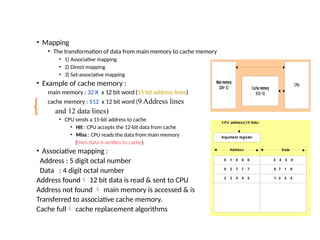
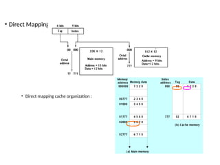
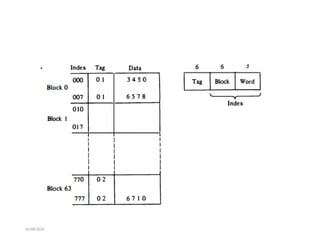
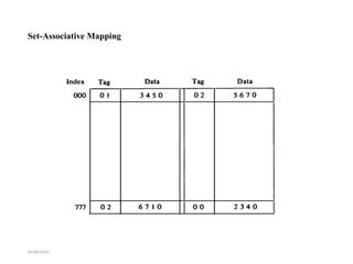
• Mapping
• Thetransformation of data from main memory to cache memory
• 1) Associative mapping
• 2) Direct mapping
• 3) Set-associative mapping
• Example of cache memory :
main memory : 32 K x 12 bit word (15 bit address lines)
cache memory : 512 x 12 bit word (9 Address lines
and 12 data lines)
• CPU sends a 15-bit address to cache
• Hit : CPU accepts the 12-bit data from cache
• Miss : CPU reads the data from main memory
(then data is written to cache)
• Associative mapping :
Address : 5 digit octal number
Data : 4 digit octal number
Address found 12 bit data is read & sent to CPU
Address not found main memory is accessed & is
Transferred to associative cache memory.
Cache full cache replacement algorithms
Main memory
32K× 12
CPU
Cache memory
512× 12
Argument register
0 1 0 0 0
2 2 3 4 5
0 2 7 7 7
3 4 5 0
1 2 3 4
6 7 1 0
Address Data
CPU address(15 bits)
In thewrite-through policy, both cache and main memory are updated with
every write operation.
In the write-back policy, only the cache is updated and the location is marked so
that it can be copied later into main memory.
• After initialization the cache is considered to be empty, but in effect it contains
some non-valid data. It is customary to include with each word in cache a valid
bit to indicate whether or not the word contains valid data.
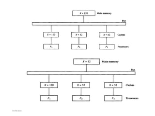
In a shared memory multiprocessor system, all the processors share a common
memory. In addition, each processor may have a local memory, part or all of
which may be a cache. The same information may reside in a number of copies
in some caches and main memory. To ensure the ability of the system to
execute memory operations correctly, the multiple copies must be kept
identical. This requirement imposes a cache coherence problem.
04/08/2025
04/08/2025
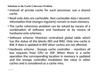
Solutions to theCache Coherence Problem
• Instead of private cache for each processor, use a shared
cache.
• Read only data are cacheable. Non cacheable data ( dynamic
information that changes regularly) remain in main memory.
• The cache coherence problem can be solved by means of a
combination of software and hardware or by means of
hardware-only schemes.
• Software scheme: Maintain centralized global table which
has the status of the blocks (RO and RW). Only one cache is
RW. If data is updated in RW other caches are not affected.
• Hardware scheme : Snoopy cache controller – monitors all
bus requests from CPU or IOP. When there is a write
operation the corresponding location in memory is updated
and the snoopy controller invalidates the value in other
caches and is considered as a cache miss.