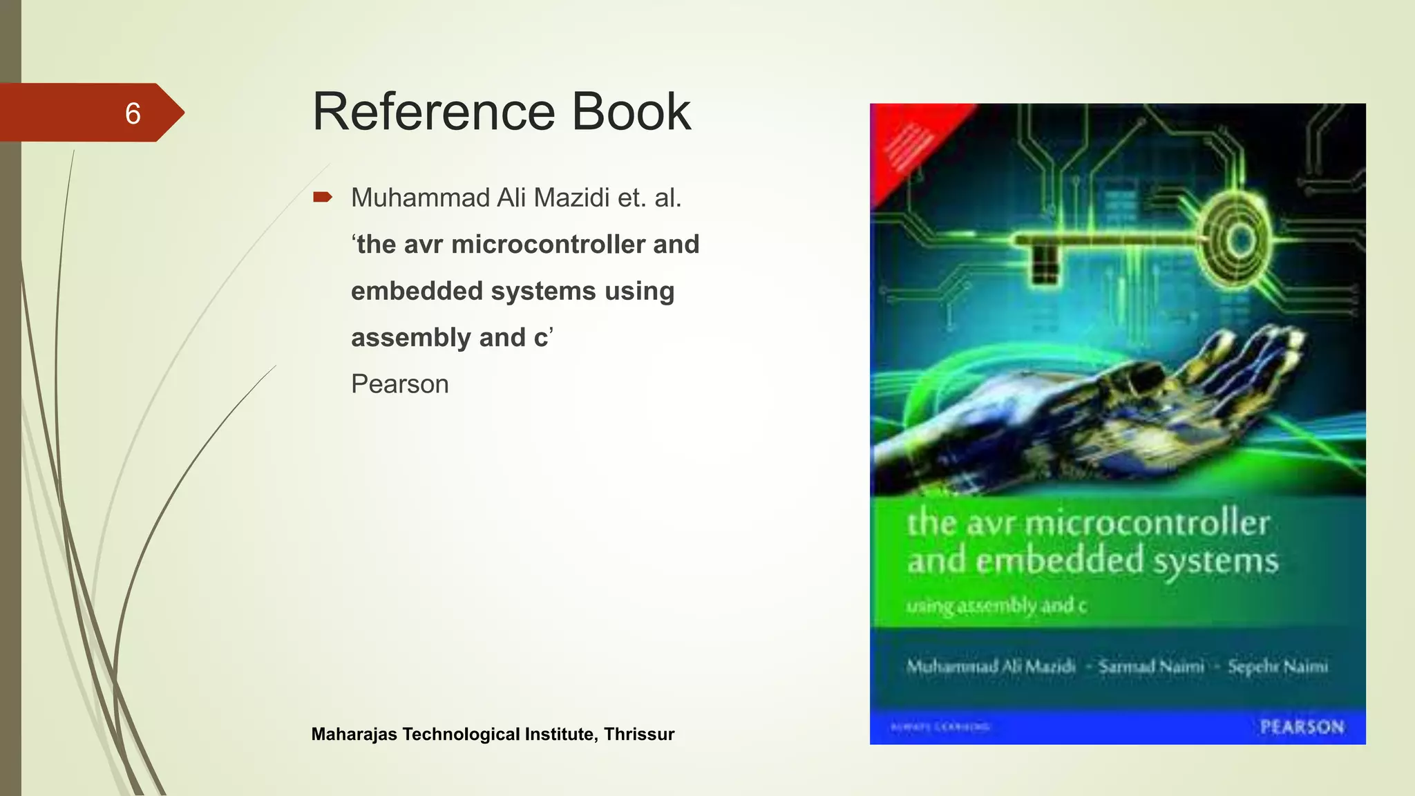
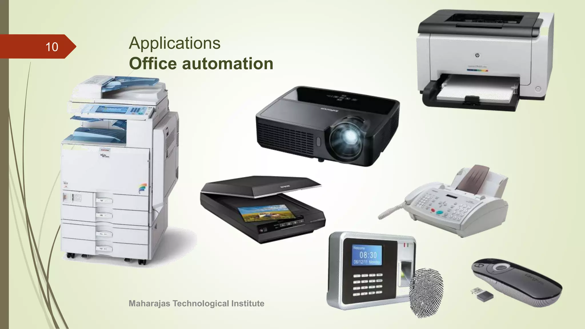
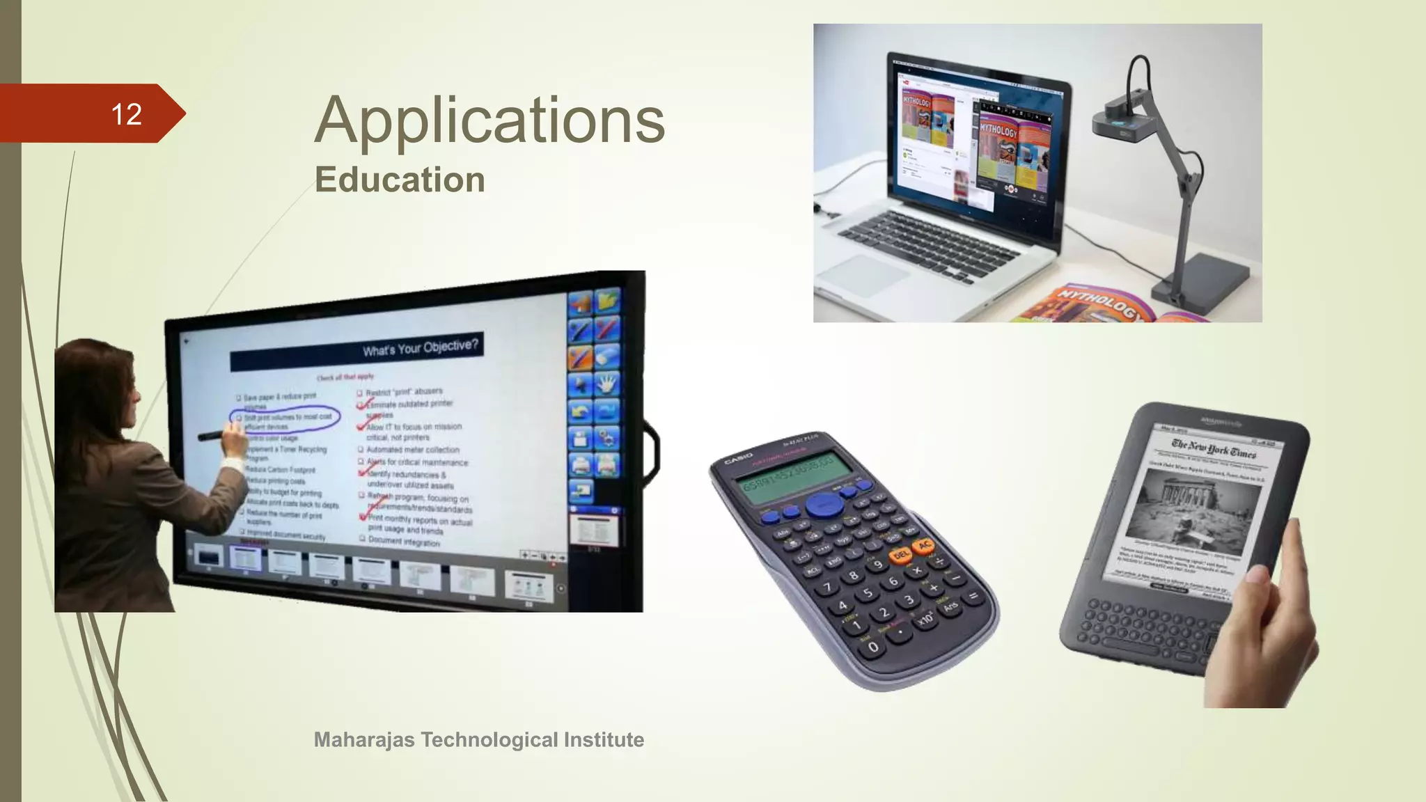
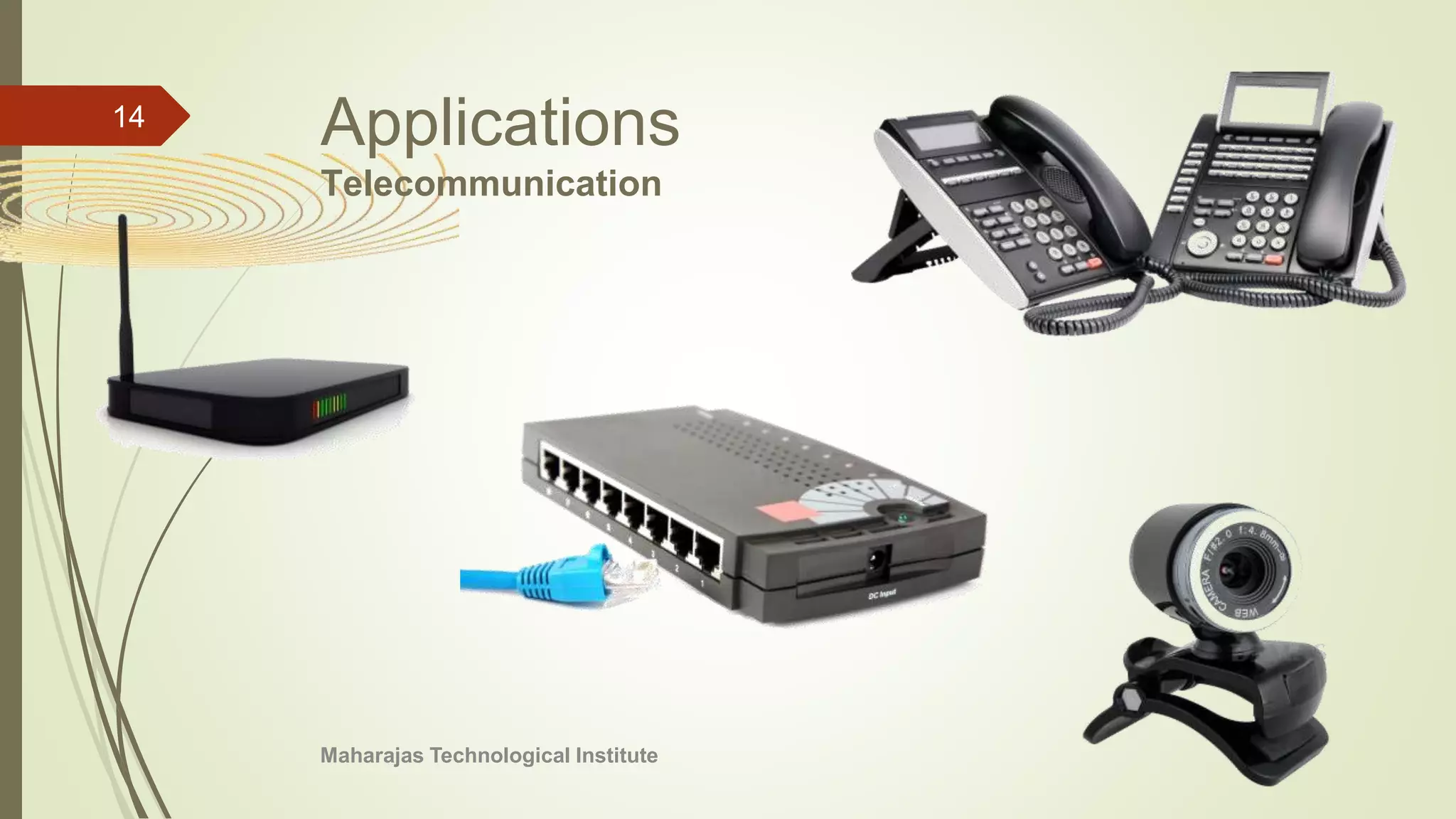
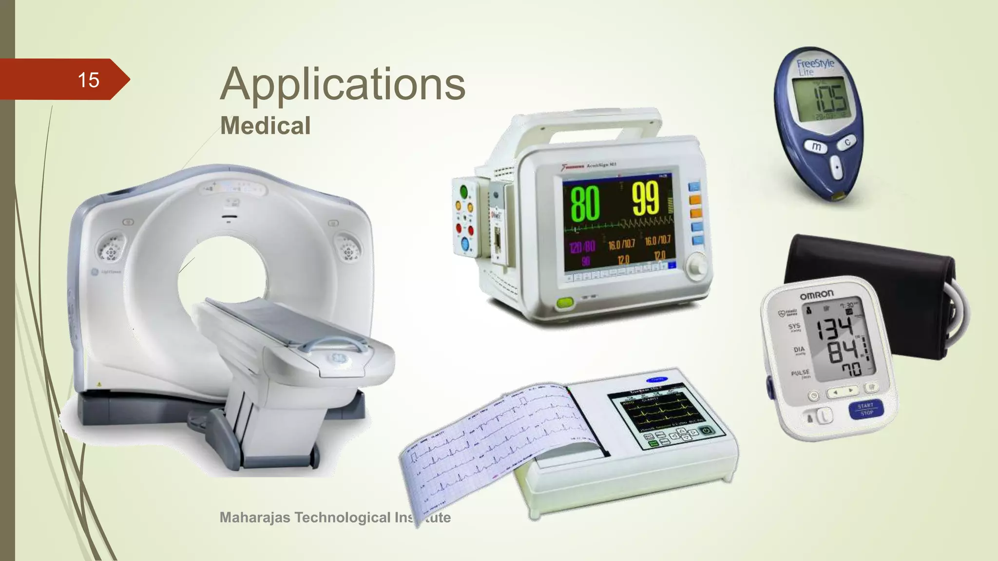
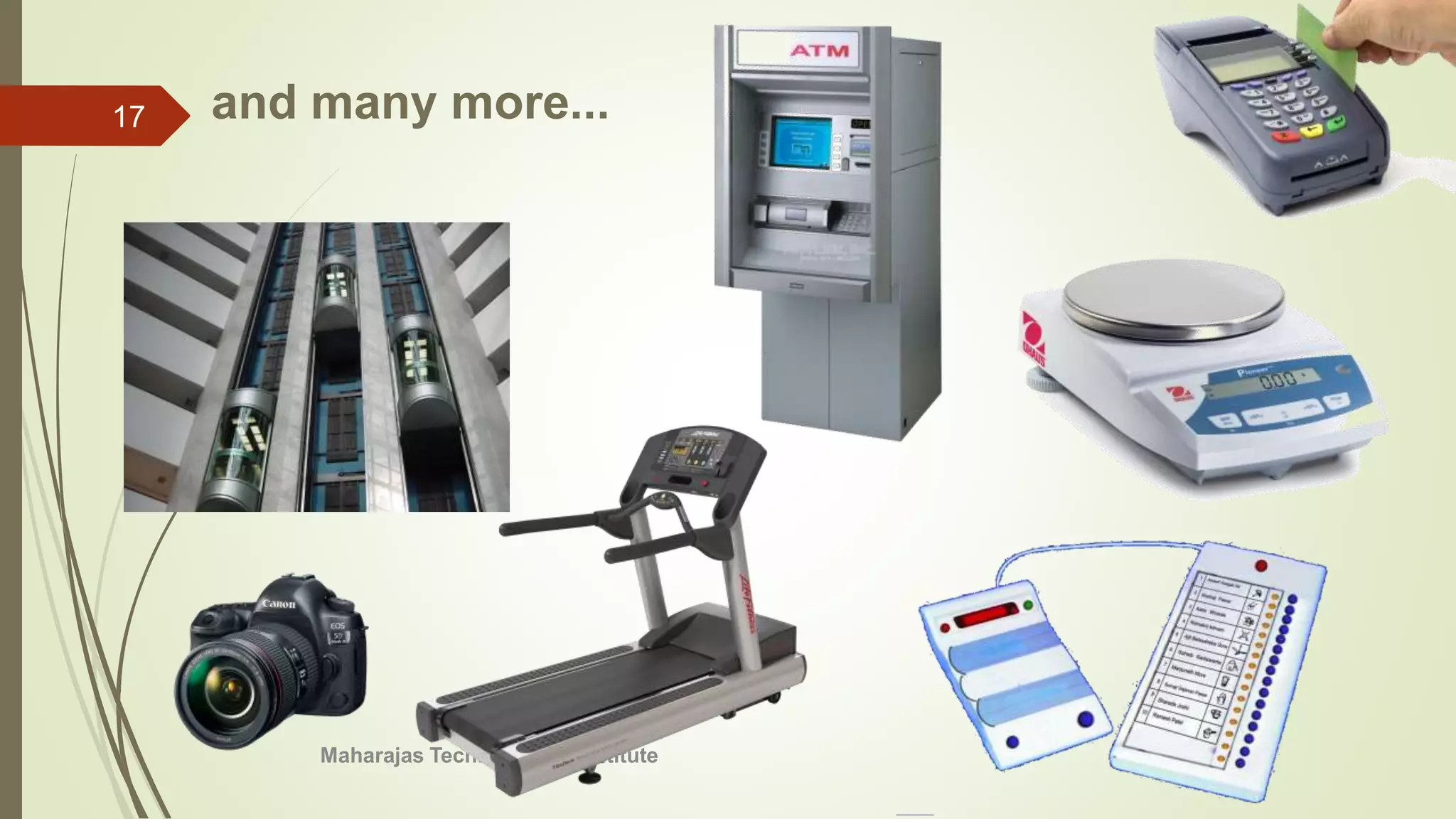
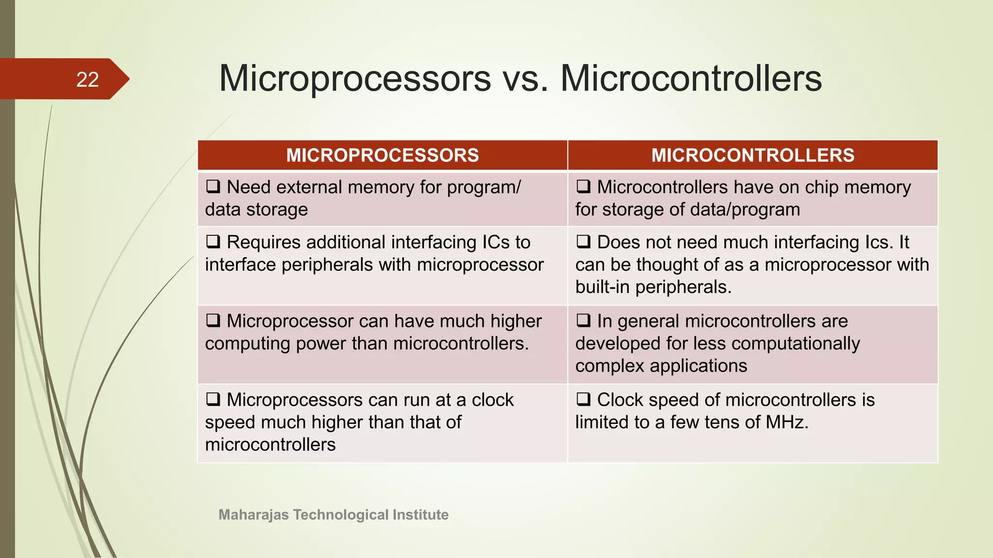
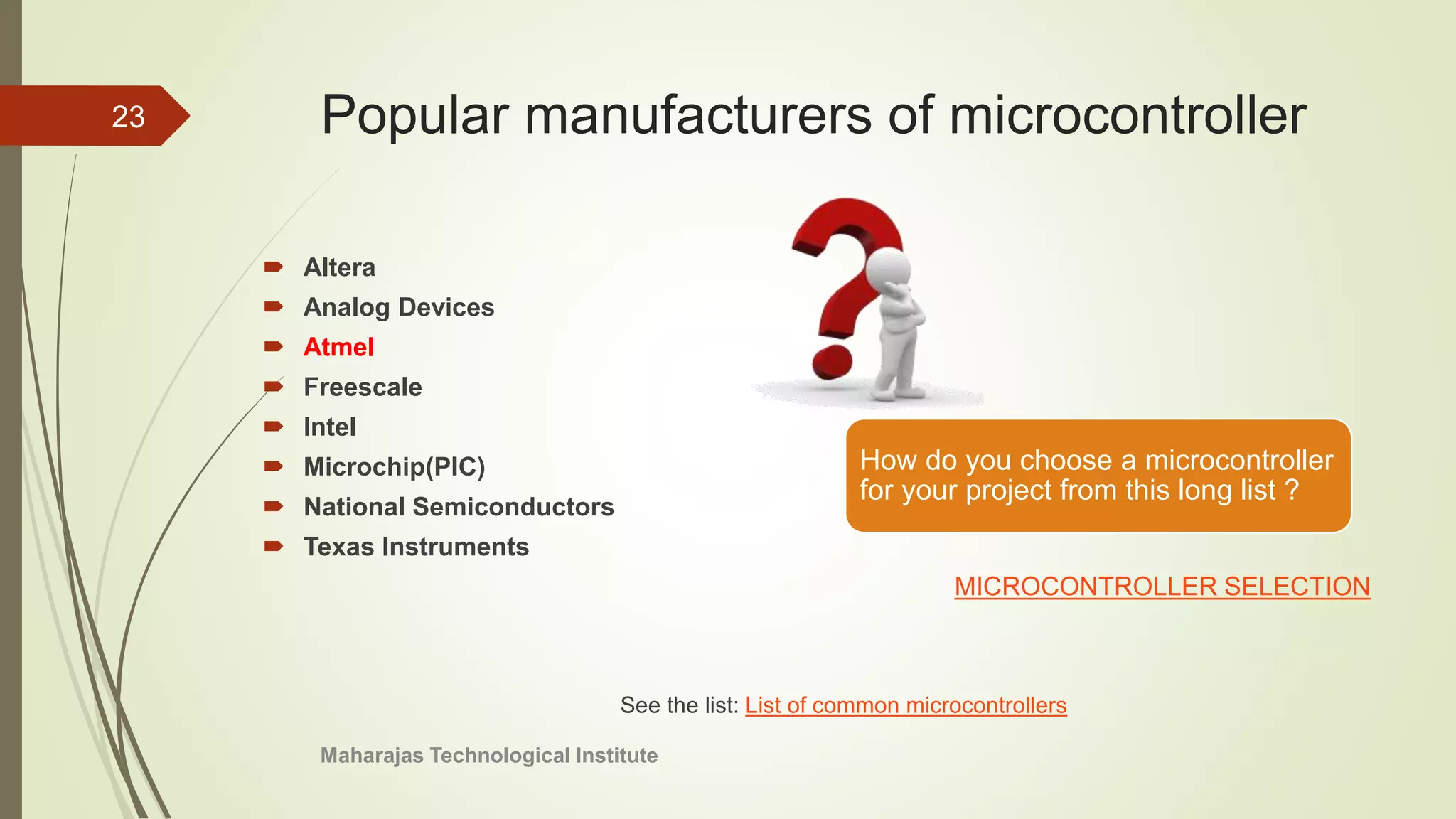
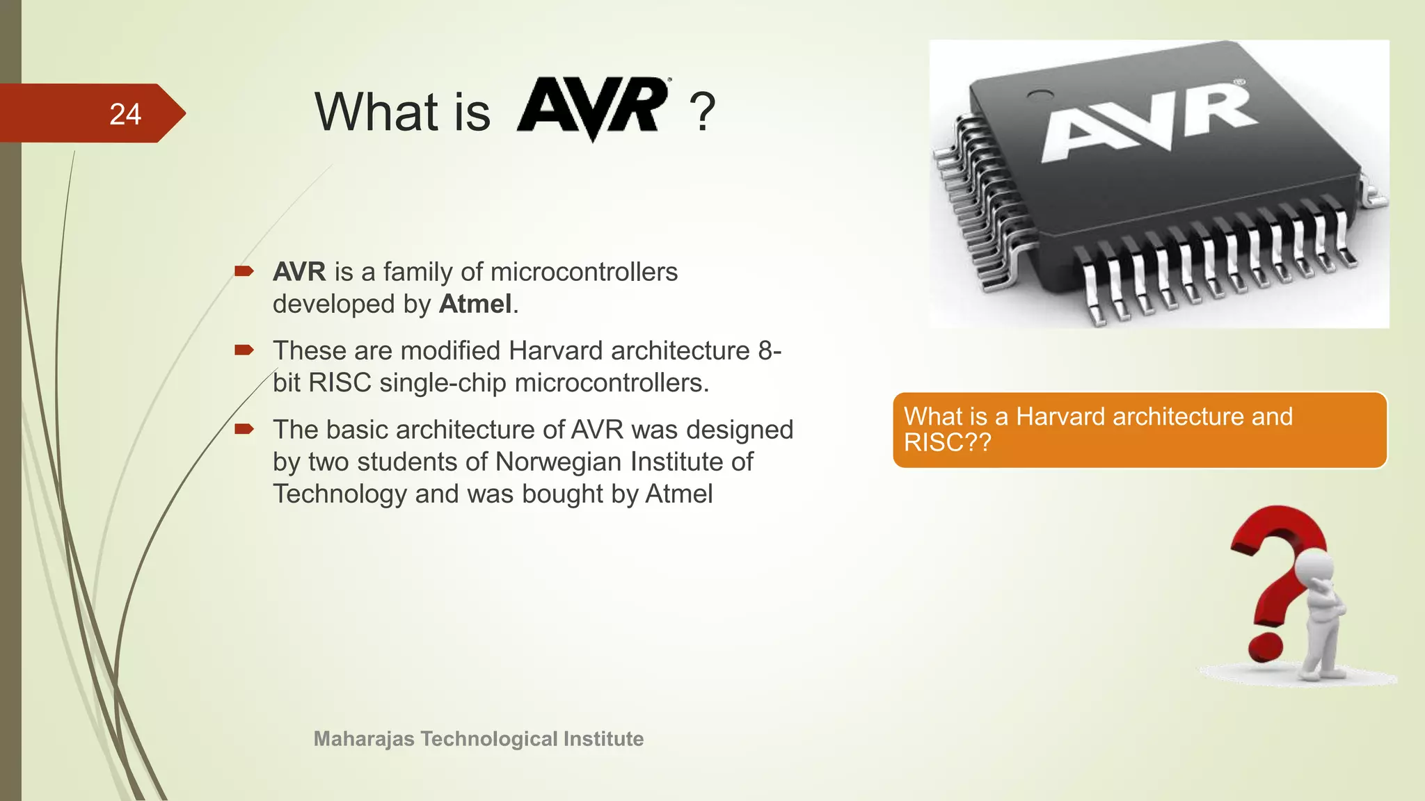
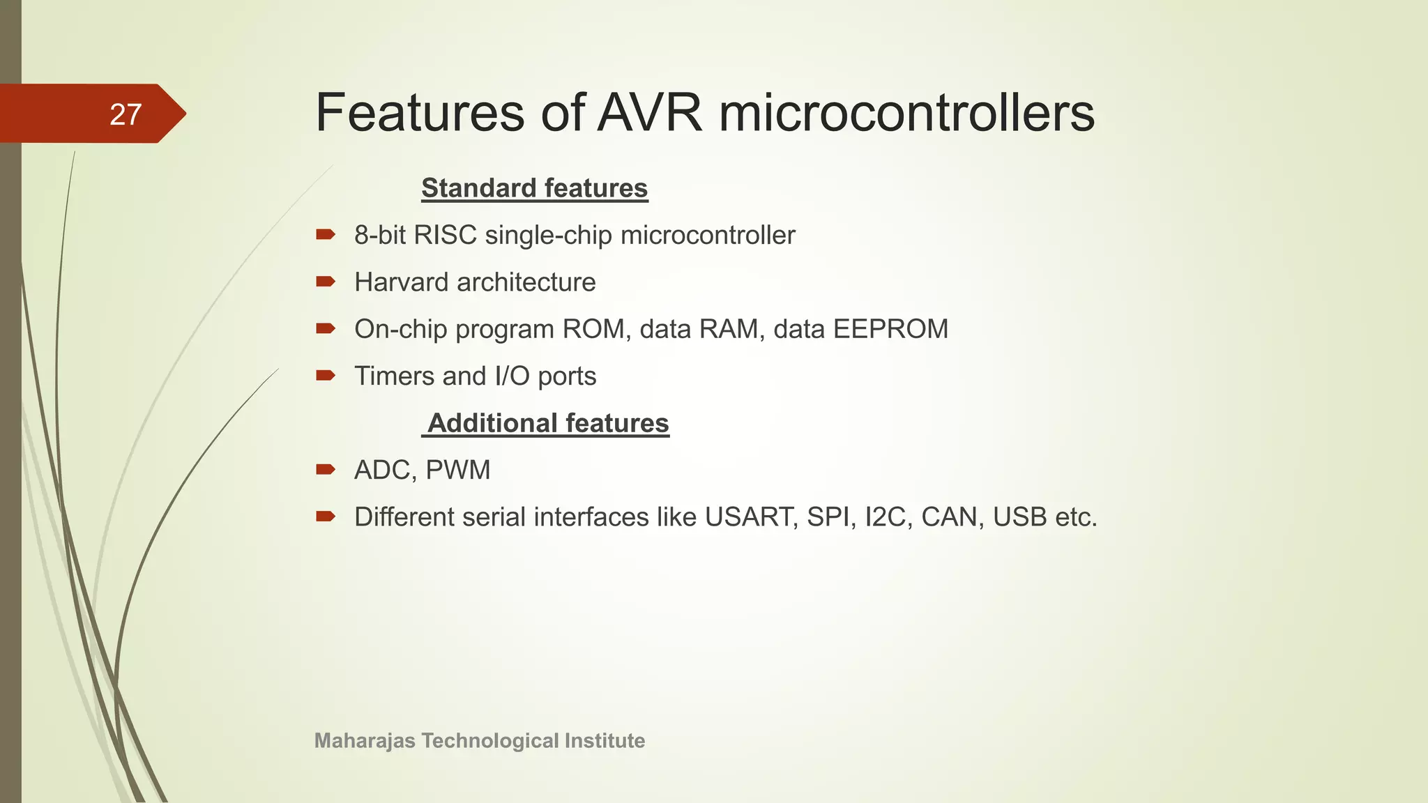
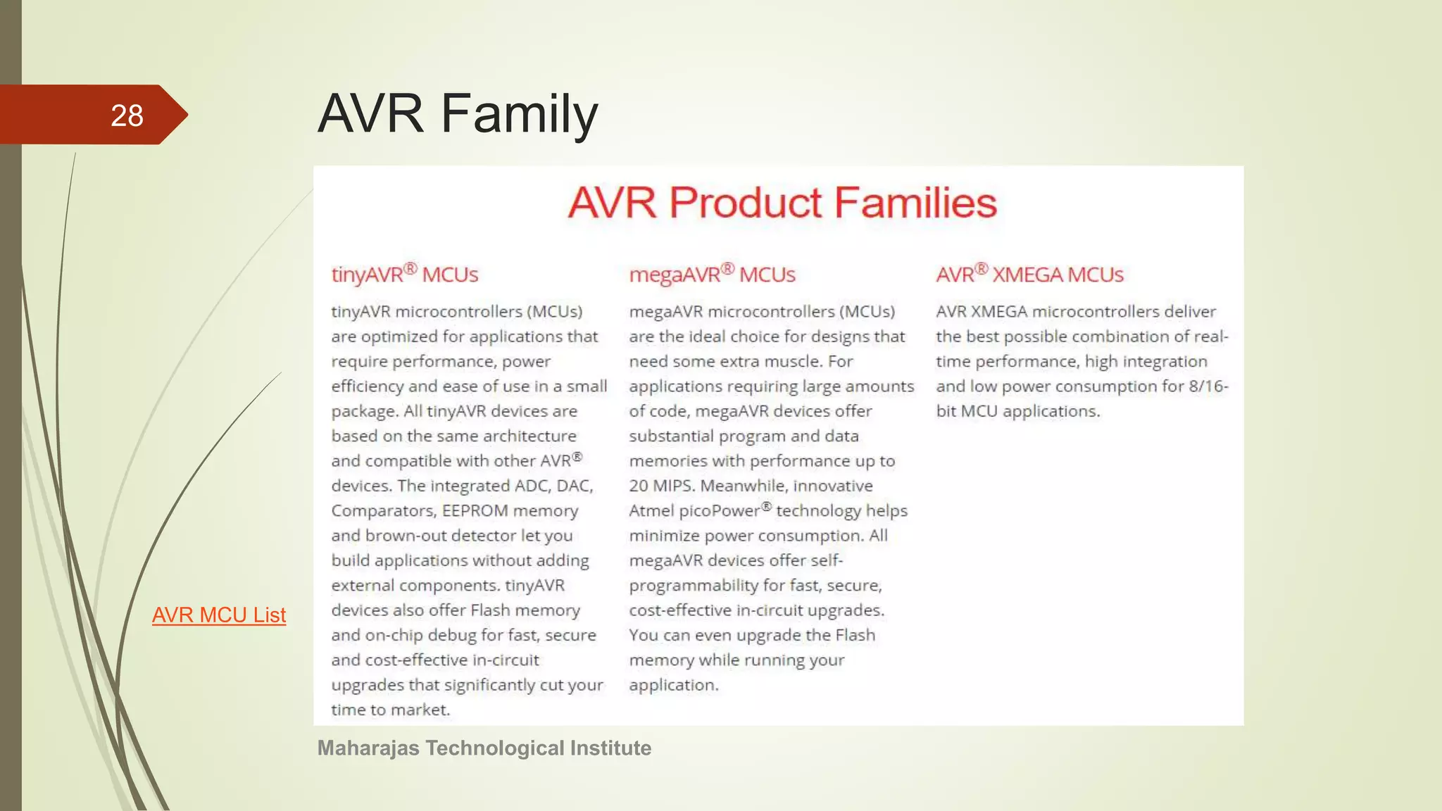
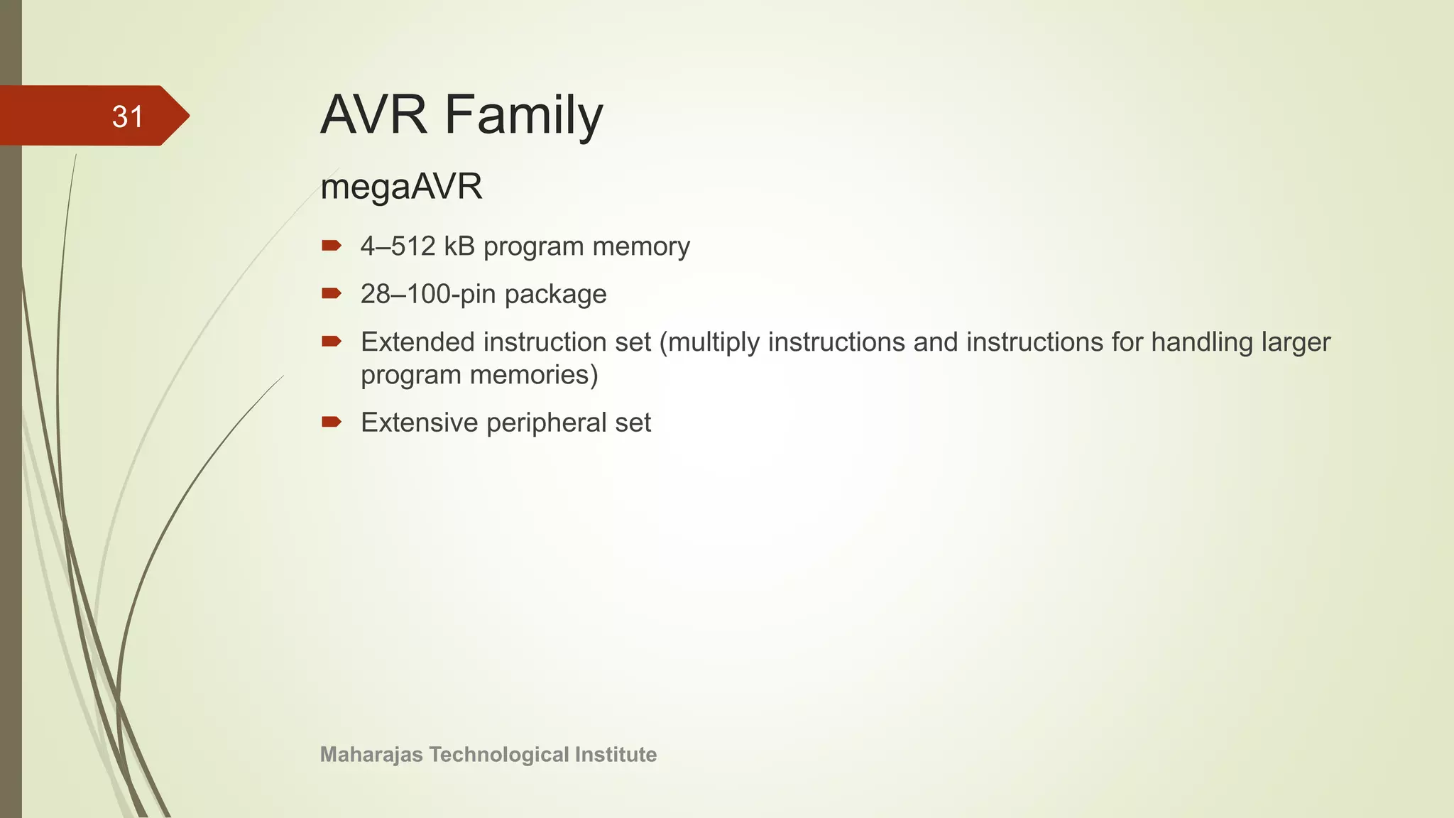
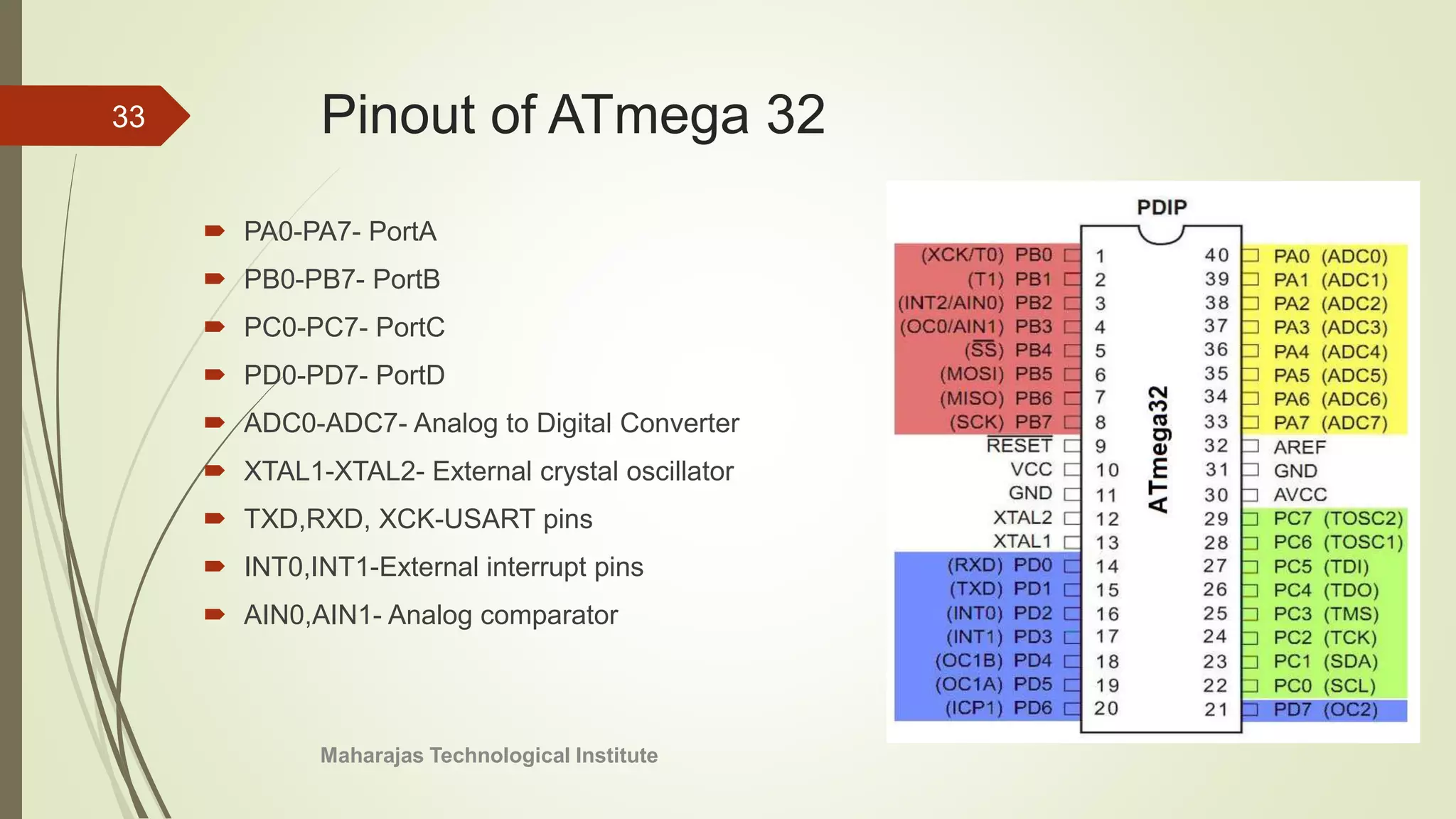
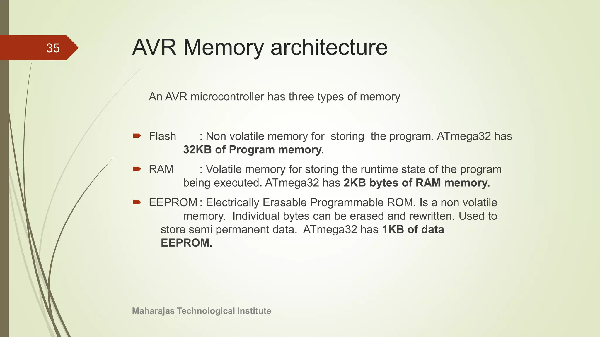
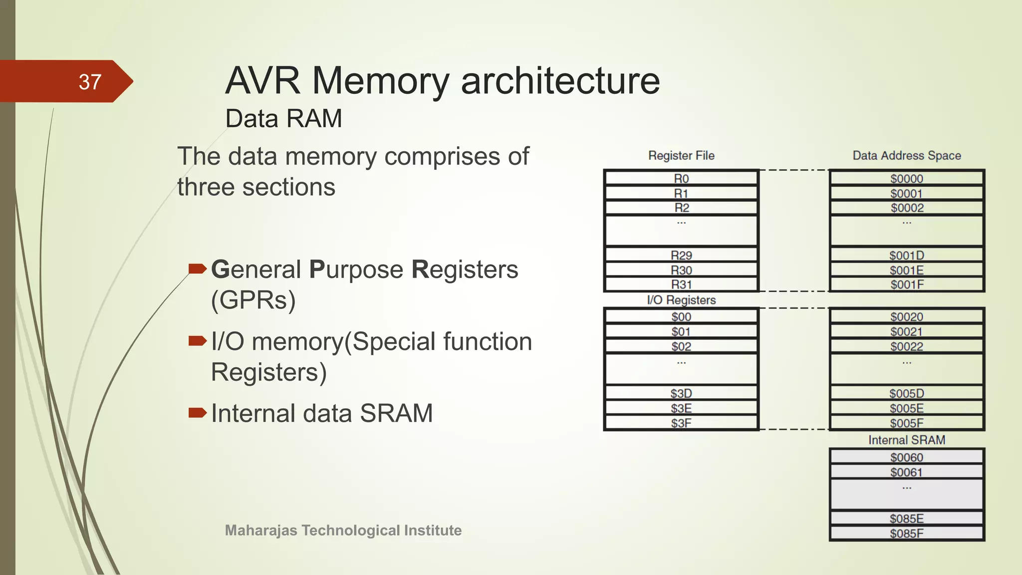
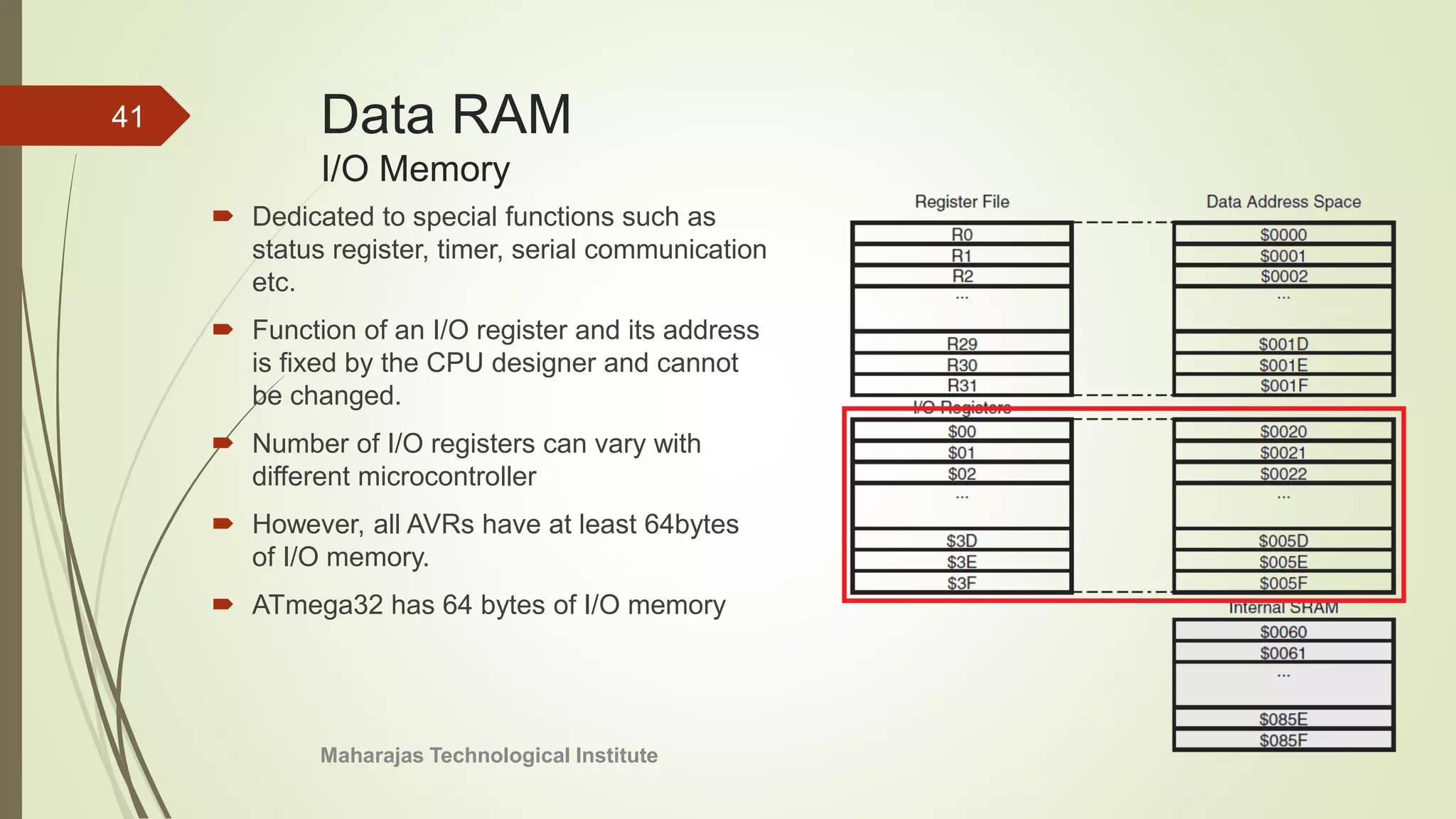
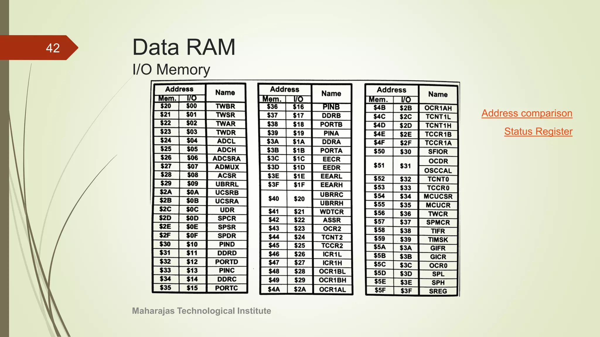
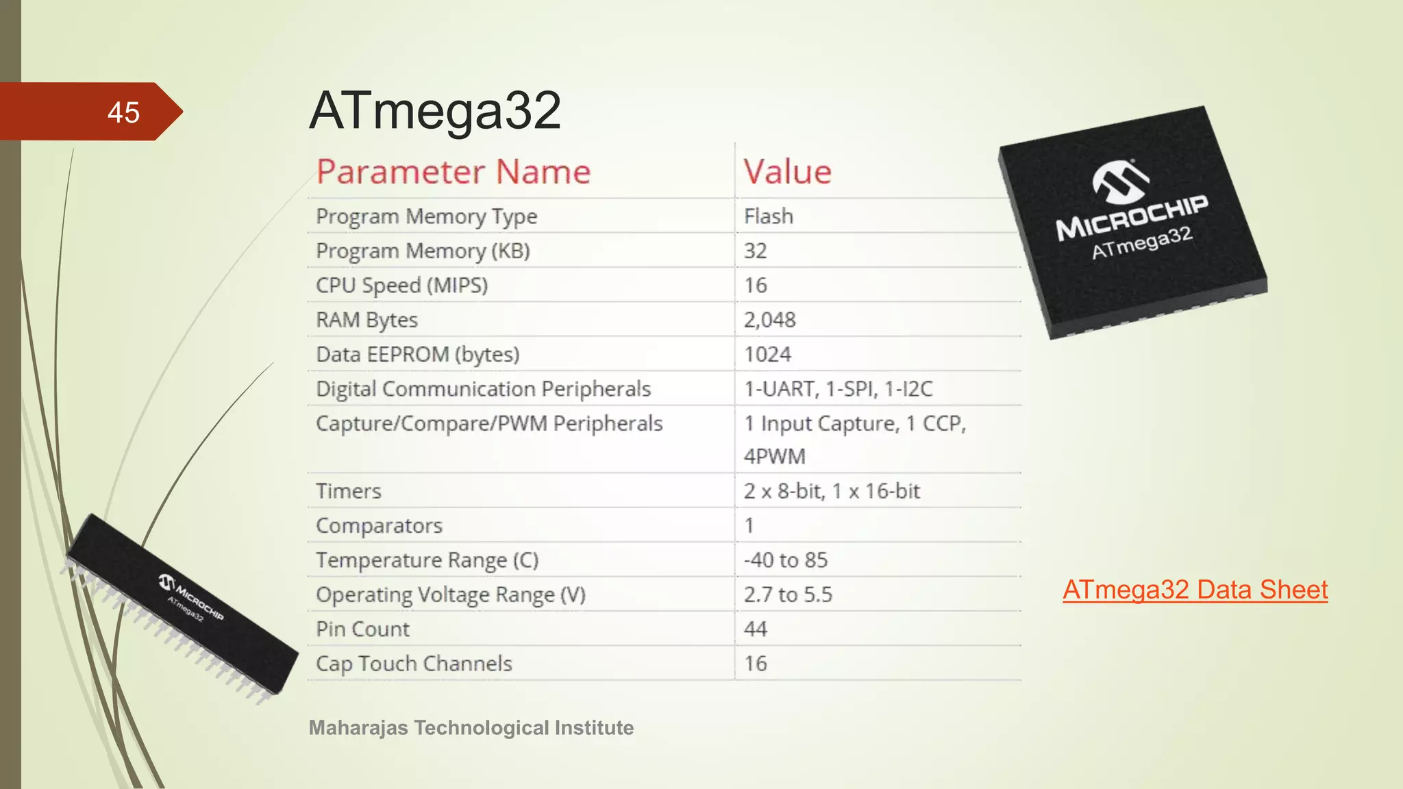
SlideShare a Scribd company logo
Embedded Systems
5041
About the course...
2
Maharajas Technological Institute, Thrissur
About the teacher
 Vineeth M P
 E-mail: vineethmpofficial@gmail.com
3
Maharajas Technological Institute
More...
 Course Code : 5041
 Number of weekly hours : 4
 Number of hours in the semester : 75( lucky if you get 35...!)
 Credits : 4
 Lab course code : 5049
 Lab hours : 5
 Lab credits : 3
 Overview of lab experiments
4
Maharajas Technological Institute
Syllabus
Module I : AVR Microcontrollers & Assembly
Language Programming
Module II: AVR Programming in C
Module III : Interfacing sub systems with AVR-I
Module IV : Interfacing sub systems with AVR-II
Maharajas Technological Institute
5
Reference Book
 Muhammad Ali Mazidi et. al.
‘the avr microcontroller and
embedded systems using
assembly and c’
Pearson
6
Maharajas Technological Institute, Thrissur
Loading...
Microcontroller
 A Microcontroller is a programmable digital processor with necessary
peripherals.
 Both microcontrollers and microprocessors are complex sequential digital
circuits meant to carry out job according to the program / instructions
 A microcontroller can be compared to a Swiss knife with multiple functions
incorporated in the same IC.
8
Maharajas Technological Institute
Applications
Home appliances
Maharajas Technological Institute
9
Applications
Office automation
Maharajas Technological Institute
10
Applications
Security
Maharajas Technological Institute
11
Applications
Education
Maharajas Technological Institute
12
Applications
Instrumentation
Maharajas Technological Institute
13
Applications
Telecommunication
Maharajas Technological Institute
14
Applications
Medical
Maharajas Technological Institute
15
Applications
Automobile
# Fuel injection controller
# security system
# Air bag
# Entertainment system
# Cruise control
# Parental control
# GPS
# Remote keyless entry
# Anti-locking breaking system
Maharajas Technological Institute
16
and many more...
Maharajas Technological Institute
17
Embedded Systems
 All the above systems fall under the
category of Emedded Systems.
 Microcontroller with built-in memory,
interfaced with peripherals
 In embedded systems, hardware units and
their controlling/ managing programs work
as a single system.
 In an embedded system, the microcontroller
work as the intelligent part controlling the
peripherals
Maharajas Technological Institute
18
What do we learn in this course ?
 In this course, we learn only about the
brain –how to program it and interface it
with peripherals
 Different sensors, display units, motors
and any other peripheral is out of scope !
 We choose AVR microcontroller as our
candidate
 Specifically ATmega32
Maharajas Technological Institute
19
AVR Microcontrollers &
Assembly Language Programming
MODULE I
Maharajas Technological Institute
20
AVR Microcontrollers & Assembly Language
Programming
AVR microcontrollers and its architecture
You learn about the basic features and architecture of avr
microcontrollers
AVR assembly language programming
You learn the instruction set and assembly language
programming(ALP) using those instructions
Maharajas Technological Institute
21
Microprocessors vs. Microcontrollers
MICROPROCESSORS MICROCONTROLLERS
 Need external memory for program/
data storage
 Microcontrollers have on chip memory
for storage of data/program
 Requires additional interfacing ICs to
interface peripherals with microprocessor
 Does not need much interfacing Ics. It
can be thought of as a microprocessor with
built-in peripherals.
 Microprocessor can have much higher
computing power than microcontrollers.
 In general microcontrollers are
developed for less computationally
complex applications
 Microprocessors can run at a clock
speed much higher than that of
microcontrollers
 Clock speed of microcontrollers is
limited to a few tens of MHz.
Maharajas Technological Institute
22
Popular manufacturers of microcontroller
 Altera
 Analog Devices
 Atmel
 Freescale
 Intel
 Microchip(PIC)
 National Semiconductors
 Texas Instruments
MICROCONTROLLER SELECTION
See the list: List of common microcontrollers
Maharajas Technological Institute
23
How do you choose a microcontroller
for your project from this long list ?
What is ?
 AVR is a family of microcontrollers
developed by Atmel.
 These are modified Harvard architecture 8-
bit RISC single-chip microcontrollers.
 The basic architecture of AVR was designed
by two students of Norwegian Institute of
Technology and was bought by Atmel
Maharajas Technological Institute
24
What is a Harvard architecture and
RISC??
About
 Atmel is an American based designer and manufacturer of
semiconductors
 It serves application including consumer, communication,
automotive, computer networking, medical and aerospace.
 In 2016 Microchip acquired Atmel
 Atmel is now knows as,
ATMEL VISIT
Maharajas Technological Institute
25
Evolution of AVR microcontroller26
Maharajas Technological Institute
Features of AVR microcontrollers
Standard features
 8-bit RISC single-chip microcontroller
 Harvard architecture
 On-chip program ROM, data RAM, data EEPROM
 Timers and I/O ports
Additional features
 ADC, PWM
 Different serial interfaces like USART, SPI, I2C, CAN, USB etc.
Maharajas Technological Institute
27
AVR Family
Maharajas Technological Institute
28
AVR MCU List
AVR Family
AVR can be classified into three groups
 Tiny
 Mega
 xmega
Maharajas Technological Institute
29
AVR Family
tinyAVR
 0.5–16 kB program memory
 6–32-pin package
 Limited peripheral set
Maharajas Technological Institute
30
AVR Family
megaAVR
 4–512 kB program memory
 28–100-pin package
 Extended instruction set (multiply instructions and instructions for handling larger
program memories)
 Extensive peripheral set
Maharajas Technological Institute
31
AVR Family
xmegaAVR
 16–384 kB program memory
 44–64–100-pin package (A4, A3, A1)
 Extended performance features, such as DMA, “Event System”, and cryptography
support.
 Extensive peripheral set with ADCs
Maharajas Technological Institute
32
Pinout of ATmega 32
Maharajas Technological Institute
33
 PA0-PA7- PortA
 PB0-PB7- PortB
 PC0-PC7- PortC
 PD0-PD7- PortD
 ADC0-ADC7- Analog to Digital Converter
 XTAL1-XTAL2- External crystal oscillator
 TXD,RXD, XCK-USART pins
 INT0,INT1-External interrupt pins
 AIN0,AIN1- Analog comparator
AVR architecture
Maharajas Technological Institute
34
 Harvard architecture-supports
parallelism
 Separate memories for program and
data
 Next instruction is fetched while current is
executed
 Fast access register file with 32x8-bit general
purpose register,
AVR Memory architecture
An AVR microcontroller has three types of memory
 Flash : Non volatile memory for storing the program. ATmega32 has
32KB of Program memory.
 RAM : Volatile memory for storing the runtime state of the program
being executed. ATmega32 has 2KB bytes of RAM memory.
 EEPROM : Electrically Erasable Programmable ROM. Is a non volatile
memory. Individual bytes can be erased and rewritten. Used to
store semi permanent data. ATmega32 has 1KB of data
EEPROM.
35
Maharajas Technological Institute
AVR Memory architecture
Maharajas Technological Institute
36
AVR Memory architecture
Data RAM
Maharajas Technological Institute
37
The data memory comprises of
three sections
General Purpose Registers
(GPRs)
I/O memory(Special function
Registers)
Internal data SRAM
Data RAM
General Purpose Registers(GPRs)
Maharajas Technological Institute
38
 There are 32 General purpose registers in
ATmega32
 Numbered from R0 to R31
 Located in the lowest location of memory
address
 All registers are 8 bit
 Used by CPU to store data temporarily
 Can be used by all arithmetic and logic
operations
Data RAM
General Purpose Registers(GPRs)
Maharajas Technological Institute
39
 The GPRs take location address from $00-$FF
in the data memory space regardless of the
AVR chip number.
 Register operations are faster.
 Fetching operands from register, performing
the operation and storing the result in memory
happens in one clock cycle
 Registers from R26 to R31 can be paired as
three 16 bit registers
AVR General Purpose Registers
Maharajas Technological Institute
40
 R26-R27  X register
 R28-R29  Y register
 R30-R31  Z register
 These registers can be used for
storing (16-bit) address of
memory locations for indirect
addressing of data
Data RAM
I/O Memory
Maharajas Technological Institute
41
 Dedicated to special functions such as
status register, timer, serial communication
etc.
 Function of an I/O register and its address
is fixed by the CPU designer and cannot
be changed.
 Number of I/O registers can vary with
different microcontroller
 However, all AVRs have at least 64bytes
of I/O memory.
 ATmega32 has 64 bytes of I/O memory
Data RAM
I/O Memory
Address comparison
Status Register
Maharajas Technological Institute
42
Data RAM
Internal data SRAM
Maharajas Technological Institute
43
 Used for storing data and parameters
 Generally called ‘scratch pad’
 Each location can be accessed by its
address.
 8 bit wide.
 Any data of 8 biy wide can be stored in it,
may it be data or address.
 Size of SRAM can vary from chip to chip.
 ATmega32 has 2KB of data SRAM.
AVR Memory
Memory of typical microcontrollers
44
Maharajas Technological Institute
ATmega32
Maharajas Technological Institute
45
ATmega32 Data Sheet
AVR Assembly language
programming
Maharajas Technological Institute
46
AVR Assembly language programming
Instruction set
Programming steps
AVR Studio 5
Maharajas Technological Institute
47
Instruction Set
Data Transfer instructions
Arithmetic and Logic instructions
Branch instructions
Bit and Bit-Test instructions
MCU control instructions
Maharajas Technological Institute
48
Data transfer instructions
MOV
 To copy data from one register to another
register
 Data can be copied only between GPRs
(R0-R31)
 Syntax : MOV Rd, Rr
 Example : MOV R10, R20
R10 R20
BEFORE $25
Maharajas Technological Institute
49
AFTER $25 $25
Data transfer instructions
LDI
 Load immediate data
 To copy 8-bit (immediate)data into
General purpose registers
 The word immediate indicates a value
that must be provided right there with the
instruction
 Syntax : LDI Rd, k
 k is an 8-bit value that can be 0-255 in
decimal
 Rd is R16 to R31
 Example : LDI R18, $4A
R18
BEFORE $4A
Maharajas Technological Institute
50
AFTER $4A
You cannot use LDI instruction to
load immediate data to registers R0 to
R15
Data transfer instructions
LDS
 Load Direct from Data Space
 To load 1 byte from an address in the data
memory to General purpose register
 Syntax : LDS Rd, K
 Load Rd with the content of location k
 Rd is R0 to R31
 Example : LDS R5, $202
 Location in data memory can be any part
of the data space. It can be an I/O
register, data SRAM or a GPR.
R05
BEFORE
Maharajas Technological Institute
51
AFTER $6C
$200 $13
$201 $FE
$202 $6C
$203 $0D
$204 $E3
$205 $19
$206 $BB
Address Data
Data transfer instructions
STS
 Store Direct to Data Space
 Syntax : STS K, Rr
 The content of register Rr is copied to the
address location K.
 Rd is R0 to R31
 Example : STS $202, R4
R04
BEFORE $A9
Maharajas Technological Institute
52
$201 $FE
$202 $3D
$203 $0D
$204 $E3
Address Data
R04
AFTER $A9
$201 $FE
$202 $A9
$203 $0D
$204 $E3
Address Data
What happens when you execute an
instruction STS 0x1, R10 ???
You cannot copy an immediate value
directly into SRAM location, but only
via a GPR...!
Data Memory address Vs I/O address53
Maharajas Technological Institute
 Each location in I/O memory has two addresses- I/O address and Data memory
address
 The data memory address of an I/O location is unique
 I/O memory address is the address relative to the beginning of I/O, called I/O
address
 In ATmega32, the data memory address can vary from $0000-$085F, but I/O
address can range from $00 to $3F
I/O memory
Data transfer instructions
IN
 Load an I/O location data to GPR
 Syntax : IN Rd, A
 0 ≤ A ≤ 63 (or $00-$3F)
 Rd is R0 to R31
 Example : IN R04, 0x3F
R04
BEFORE
Maharajas Technological Institute
54
$3C $FE
$3D $3D
$3E $0D
$3F $E3
I/O Address Data
R04
AFTER $E3
$3C $FE
$3D $3D
$3E $0D
$3F $E3
I/O Address Data
If both LDS and IN instructions copy
data from data memory to GPR, then
what is the difference between them?
Data transfer instructions
OUT
 Store the GPR into an I/O register
 Syntax : OUT A, Rr
 0 ≤ A ≤ 63 (or $00-$3F)
 Rr is R0 to R31
 Example : OUT $3C, R04
R04
BEFORE $AA
Maharajas Technological Institute
55
$3C $FE
$3D $3D
$3E $0D
$3F $E3
I/O Address Data
R04
AFTER $AA
$3C $AA
$3D $3D
$3E $0D
$3F $E3
I/O Address Data
Data transfer instructions
LD
 Load Indirect
 To load 1 byte from an address pointed by
the GPR pair(X,Y,Z)
 Syntax : LD Rd,m
 Load Rd with the content of address
pointed by m
 m can be X,Y or Z
 Example : LD R5, Y
 Location in data memory can be any part
of the data space. It can be an I/O
register, data SRAM or a GPR.
R05
BEFORE
Maharajas Technological Institute
56
AFTER $0D
$0232 $13
$0233 $FE
$0234 $6C
$0235 $0D
$0236 $E3
$0237 $19
$0238 $BB
Address Data
$02 $35
R29=YH R28=YL
Data transfer instructions
ST
 Load Indirect
 To load 1 byte from an address pointed by
the GPR pair(X,Y,Z)
 Syntax : ST m, Rr
 Store the content of Rr to the address
pointed by m
 m can be X,Y or Z
 Example : ST Y, R05
 Location in data memory can be any part
of the data space. It can be an I/O
register, data SRAM or a GPR.
Instruction set
R05
BEFORE $0D
Maharajas Technological Institute
57
$0232 $13
$0233 $FE
$0234 $6C
$0235 $0D
$0236 $E3
$0237 $19
$0238 $BB
Address Data
$02 $33
R27=YH R26=YL
$0232 $13
$0233 $0D
$0234 $6C
$0235 $0D
$0236 $E3
$0237 $19
$0238 $BB
R05
AFTER $0D
Data transfer instructions
Example No.1
LDI R20, $18
MOV R19, R20
LDI R20, $2A
MOV R19, R20
STS $237, R19
Maharajas Technological Institute
58
Address Data
$0232 $13
$0233 $21
$0234 $6C
$0235 $0D
$0236 $E3
$0237 $19
$0238 $BB
R19
$18
R20
$18 $18$18 $2A$2A $2A $0232 $13
$0233 $21
$0234 $6C
$0235 $0D
$0236 $E3
$0237 $2A
$0238 $BB
Data transfer instructions
Example No.2
LDS R23, $233
LDI R22, $7E
MOV R23, R22
STS $237,R23
Maharajas Technological Institute
59
Address Data
$0232 $13
$0233 $21
$0234 $6C
$0235 $0D
$0236 $E3
$0237 $19
$0238 $BB
R22
$21
R23
$7E $21
$7E $7E
$0232 $13
$0233 $21
$0234 $6C
$0235 $0D
$0236 $E3
$0237 $7E
$0238 $BB
Data transfer instructions
Example No.3
LDI R28, $38
LDI R29, $02
ST Y, R20
Maharajas Technological Institute
60
Address Data
$0232 $13
$0233 $21
$0234 $17
$0235 $0D
$0236 $E3
$0237 $19
$0238 $BB
R29
$38
R28
$02 $38
$0232 $13
$0233 $21
$0234 $17
$0235 $0D
$0236 $E3
$0237 $19
$0238 $FB
R20
$FB
Data transfer instructions
Example No.4
LDI R26, $38
LDI R27, $02
LD R28, X
Maharajas Technological Institute
61
Address Data
$0232 $13
$0233 $21
$0234 $6C
$0235 $0D
$0236 $E3
$0237 $19
$0238 $BB
R27
$38
R26
$02 $38
R20
$BB
$02
Data transfer instructions
Find the errors in the following instructions
LDI R20, $202
LDS R19, R16
LDI R09, $55
LDS R21, y
Maharajas Technological Institute
62
A 12 bit number cannot go into an 8 bit
register
LDS is used to load data from memory, not
from another register-syntax error
LDI cannot load an immediate data into
registers from R0-R15
Wrong instruction. Use LD instead of LDS
AVR Status Register-SREG
 Flag register to indicate arithmetic conditions such as carry bit
 Flag register in AVR is called Status Register – SREG
 An 8-bit register
 In ATmega32 SREG has data memory address of $5F and I/O address of $3F
 The function of each bit is as follows...
I/O Memory
63
Maharajas Technological Institute
I T H S V N Z C
D2 D1D4 D3 D0D5D6D7
SREG($5F)
AVR Status Register-SREG
C- Carry flag
I T H S V N Z C
 C flag is set whenever there is a carry out from the D7th bit
 The flag is affected after an 8 bit addition or subtraction
 Is used to detect errors in unsigned arithmetic operation
Maharajas Technological Institute
64
D2 D1D4 D3 D0D5D6D7
AVR Status Register-SREG
Z- Zero flag
I T H S V N Z C
 The zero flag reflects the result of an arithmetic or logic operation
 If the result is zero then Z=1 or
 Z=1 if result is not zero
Maharajas Technological Institute
65
D2 D1D4 D3 D0D5D6D7
AVR Status Register-SREG
N- Negative flag
I T H S V N Z C
 Negative flag reflects the result of an arithmetic operation
 If D7th bit of the result is zero then N=0
 If the D7th bit is 1 then N=1
Maharajas Technological Institute
66
D2 D1D4 D3 D0D5D6D7
AVR Status Register-SREG
V- Overflow flag
I T H S V N Z C
 Whenever the result of a signed number operation is too large, and the high-order
bit overflows into the sign bit(D7th bit), V flag is set.
 Used to detect errors in signed arithmetic operation
Maharajas Technological Institute
67
D2 D1D4 D3 D0D5D6D7
AVR Status Register-SREG
S- Sign flag
I T H S V N Z C
 This flag is the result of EX-Oring of N and V flags.
Maharajas Technological Institute
68
D2 D1D4 D3 D0D5D6D7
AVR Status Register-SREG
H- Half carry flag
I T H S V N Z C
 Sets whenever there is a carry from D3 to D4 during ADD or SUB operation.
 Used in BCD arithmetic.
 Function same as that of Auxiliary carry flag in some microprocessors
Maharajas Technological Institute
69
D2 D1D4 D3 D0D5D6D7
Arithmetic and logic instructions
ADD
 Adds the content of two registers
 Syntax : ADD Rd, Rr
 Flags affected: C,Z,H, S,V,N
 Example: ADD R21,R22
Maharajas Technological Institute
70
R21 R22
BEFORE $15 $25
AFTER $3A $25
Arithmetic and logic instructions
ADC
 Adds the content of two registers
along with carry
 Syntax : ADC Rd, Rr
 Flags affected: C,Z,H, S,V,N
 Example: ADC R21,R22
Maharajas Technological Institute
71
R21 R22
BEFORE $15 $25
AFTER $3B $25
1
N ZS V CHTI
Arithmetic and logic instructions
SUB
 Subtracts the content of source
register from destination register and
stores it back to destination register
 Syntax : SUB Rd, Rr
 Flags affected: Z,C,N,V,H
 Example: SUB R21,R22
Maharajas Technological Institute
72
R21 R22
BEFORE $34 $13
AFTER $11 $13
Arithmetic and logic instructions
SUBI
 Subtracts a constant from register
content
 Syntax : SUB Rd, k
 Flags affected: Z,C,N,V,H
 Example: SUB R16,$0A
Maharajas Technological Institute
73
R16
BEFORE $3A
AFTER $30
Arithmetic and logic instructions
SBC
 Subtract the content of source
register and carry from destination
register
 Rd=Rd-Rr-C
 Syntax : SBC Rd, Rr
 Flags affected: C,Z,H, S,V,N
 Example: SBC R21,R22
Maharajas Technological Institute
74
R21 R22
BEFORE $25 $15
AFTER $0F $15
1
N ZS V CHTI
Arithmetic and logic instructions
AND
 Logical AND registers
 Syntax : AND Rd, Rr
 Flags affected: Z,V,N
 Example: AND R21,R22
Maharajas Technological Institute
75
0 1 0 1 0 0 1 1R21=$53
1 1 1 1 0 0 0 0
R22=$F0
0 1 0 1 0 0 0 0
R21=$50
Arithmetic and logic instructions
ANDI
 Logical AND register and a constant
 Syntax : ANDI Rd, k
 k is an 8 bit number
 Flags affected: Z,V,N
 Example: ANDI R21,$17
Maharajas Technological Institute
76
0 1 0 1 0 0 1 1R21=$53
0 0 0 1 0 1 1 1
$17
0 0 0 1 0 0 1 1
R21=$13
Arithmetic and logic instructions
OR
 Logical OR registers
 Syntax : OR Rd, Rr
 Flags affected: Z,V,N
 Example: OR R21,R22
Maharajas Technological Institute
77
0 1 0 0 0 0 1 1R21=$43
0 0 0 1 0 0 0 0
R22=$10
0 1 0 1 0 0 1 1
R21=$53
Arithmetic and logic instructions
ORI
 Logical OR register and a constant
 Syntax : ORI Rd, k
 K is an 8 bit number
 Flags affected: Z,V,N
 Example: ORI R21,$17
Maharajas Technological Institute
78
0 1 0 1 0 0 1 1R21=$53
0 0 0 1 0 1 1 1
$17
0 1 0 1 0 1 1 1
R21=$57
Arithmetic and logic instructions
EOR
 Exclusive ORing of registers
 Syntax : EOR Rd, Rr
 Flags affected: Z,V,N
 Example: EOR R21,R22
Maharajas Technological Institute
79
1 1 0 1 0 0 1 1R21=$D3
1 0 1 0 1 0 1 0
R22=$A
A
0 1 1 1 1 0 0 1
R21=$79
Arithmetic and logic instructions
COM
 1’s complement of registers
 Syntax : COM Rd
 Flags affected: Z,C,V,N
 Example: COM R21
Maharajas Technological Institute
80
0 1 0 1 0 1 0 1R21=$55
1 0 1 0 1 0 1 0
R21=$A
A
BEFORE
AFTER
Arithmetic and logic instructions
NEG
 2’s complement of registers
 Syntax : NEG Rd
 Flags affected: Z,C,V,N,H
 Example: NEG R21
Maharajas Technological Institute
81
0 1 0 1 0 1 0 1R21=$55
1 0 1 0 1 0 1 1
R21=$A
B
BEFORE
AFTER
Arithmetic and logic instructions
INC
 Increment register value by 1
 Syntax : INC Rd
 Flags affected: Z,V,N
 Example: INC R21
Maharajas Technological Institute
82
0 1 0 1 0 1 0 1R21=$55
0 1 0 1 0 1 1 0
R21=$56
BEFORE
AFTER
Arithmetic and logic instructions
DEC
 Decrement register value by 1
 Syntax : DEC Rd
 Flags affected: Z,V,N
 Example: DEC R21
Maharajas Technological Institute
83
0 1 0 1 0 1 0 1R21=$55
0 1 0 1 0 1 0 0
R21=$54
BEFORE
AFTER
Arithmetic and logic instructions
CLR
 Clear register
 Syntax : CLR Rd
 Flags affected: Z,V,N
 Example: CLR R21
Maharajas Technological Institute
84
0 1 0 1 0 1 0 1R21=$55
0 0 0 0 0 0 0 0
R21=$00
BEFORE
AFTER
Arithmetic and logic instructions
SER
 Set register
 Syntax : SER Rd
 Flags affected: None
 Example: SER R21
Maharajas Technological Institute
85
0 1 0 1 0 1 0 1R21=$55
1 1 1 1 1 1 1 1
R21=$FF
BEFORE
AFTER
Arithmetic and logic instructions
MUL
 Multiplies the content of two registers
and stores the result in R0 and R1
 Syntax : MUL Rd, Rr
 Flags affected: C,Z
 Example: MUL R21,R22
Maharajas Technological Institute
86
R21 R22
BEFORE $15 $25
R1 R0
AFTER $01 $77
Bit and bit-test instructions
SBI
 Set bit in I/O register
 Syntax : SBI P, b
 Flags affected: None
 Example SBI DDRA, 2
Maharajas Technological Institute
87
0 0 0 0 0 0 0 0DDRA
0 0 0 0 0 1 0 0
DDRA
BEFORE
AFTER
D2 D1D4 D3 D0D5D6D7
D2 D1D4 D3 D0D5D6D7
Bit and bit-test instructions
CBI
 Clear bit in I/O register
 Syntax : CBI P, b
 Flags affected: None
 Example CBI DDRA, 2
Maharajas Technological Institute
88
1 1 1 1 1 1 1 1DDRA
1 1 1 1 1 0 1 1
DDRA
BEFORE
AFTER
D2 D1D4 D3 D0D5D6D7
D2 D1D4 D3 D0D5D6D7
Bit and bit-test instructions
LSL
 Logical Shift Left
 Shifting the content of given register by 1 bit
 Syntax : LSL Rd
 Flags affected: Z,C,N,V
 Example LSL R18
Maharajas Technological Institute
89
1 0 0 0 1 1 0 1R18
0 0 0 1 1 0 1 0R18
BEFORE
AFTER
0
Bit and bit-test instructions
LSR
 Logical Shift Right
 Shifting the content of register right by 1 bit
 Syntax : LSR Rd
 Flags affected: Z,C,N,V
 Example LSR R18
Maharajas Technological Institute
90
1 0 0 0 1 1 0 1R18
0 1 0 0 0 1 1 0R18
BEFORE
AFTER
0
Bit and bit-test instructions
ROL
 Rotate left through Carry
 Syntax : ROL Rd
 Flags affected: Z,C,N,V
 Example ROL R18
Maharajas Technological Institute
91
0 0 0 0 1 1 0 1R18
0 0 0 1 1 0 1 1R18
BEFORE
AFTER
1
0
C
C
Bit and bit-test instructions
ASR
 Aritmetic Shift Right
 Shifting the content of register right by 1 bit
 Syntax : LSR Rd
 Example LSR R18
 Flags affected: Z,C,N,V
 The D7th bit is filled with the same
value of D7th bit just before
shifting
Maharajas Technological Institute
92
1 0 0 0 1 1 0 1R18
1 1 0 0 0 1 1 0R18
BEFORE
AFTER
0
Bit and bit-test instructions
SWAP
 Swap nibbles.
 When this instruction is executed
on a register the lower 4 bits and
upper 4 bits are exchanged ie,
D3-D0 bits become D7-D4 and
D7-D4 bits become D3-D0
 Syntax : SWAP Rd
 Flags affected: None
 Example: SWAP R20
Maharajas Technological Institute
93
1 1 1 1 0 0 0 0
R20=$F0
R20=$0F
BEFORE
AFTER
0 0 0 0 1 1 1 1
Bit and bit-test instructions
SEC
 Set carry
 The carry bit in the status register is cleared
 No operands
 Flags affected : C
 Syntax : CLC
Maharajas Technological Institute
94
0 1 0 1 0 1 1 0
0 1 0 1 0 1 1 1
BEFORE
AFTER
SREG
SREG
I T H S V N Z C
I T H S V N Z C
Bit and bit-test instructions
CLC
 Clear carry
 The carry bit in the status register is cleared
 No operands
 Flags affected : C
 Syntax : CLC
Maharajas Technological Institute
95
0 1 0 1 0 1 0 1
0 1 0 1 0 1 0 0
BEFORE
AFTER
SREG
SREG
I T H S V N Z C
I T H S V N Z C
Instructions we learnt so far...
Data Transfer
Instruction
Arithmetic
and Logic
instructions
Arithmetic
and Logic
instructions
Bit and Bit-
Test
instructions
MCU Control
Instructions
MOV ADD COM SBI NOP
LDI ADC NEG CBI
LDS SUB INC LSL
STS SUBI DEC LSR
IN SBC CLR ROL
OUT AND SER ASR
LD ANDI MUL SWAP
ST OR SEC
MOV ORI CLC
EOR
96
Maharajas Technological Institute
MCU control instructions
NOP
 No operation is done
 No operand
 No flag is affected
 One unit of clock cycle is used out
 Can generate a delay
Maharajas Technological Institute
97
Some Examples...
Example No. 5
LDI R17, $33
LDI R18, $21
INC R17
INC R17
DEC R18
ADD R17,R18
STS $65, R17
98
Maharajas Technological Institute
Find the contents of the
registers and Location $65
Some Examples...
Example No. 6
LDI R17, $9F
LDI R18, $61
CLR R19
ADD R17, R18
ROL R17
Find the contents of the registers
99
Maharajas Technological Institute
Some Examples...
Example No. 7
LDI R17, $90
LDI R18, $30
SWAP R17 Find the contents of the registers
SWAP R18
MUL R17, R18
MOV R17,R0
MOV R18,R1
100
Maharajas Technological Institute
Some Examples...
Example No. 8
LDI R17, $90
LDI R18, $30
ASR R17
ASR R18
COM R17
NEG R18
101
Maharajas Technological Institute
Some Examples...
Example No. 8
Write an assembly language program for
subtracting two 8 bit numbers and store the
difference in memory
102
Maharajas Technological Institute
Some Examples...
Example No. 9
Write an assembly language program for
multiplying two 8 bit numbers and store the
product in memory
103
Maharajas Technological Institute
Some Examples...
Example No. 10
Write an assembly language program to add
two 16-bit numbers and store the sum and
carry in memory
104
Maharajas Technological Institute
Branching instructions
To change the sequential flow of program execution
Classified as two types
Conditional Branching Instructions
Unconditional Branching Instructions
105
Maharajas Technological Institute
Conditional Branching instructions
BRNE
 Branch if NOT EQUAL
 It can be read as ‘branch if not equal to
zero’
 Checks whether Z flag is set(Z=1) and
branches if not (Z=0)
Back: ……….
……….
……….
DEC R16
BRNE Back
……….
106
Maharajas Technological Institute
Conditional Branching instructions
BREQ
 Branch if EQUAL
 It can be read as ‘branch if equal to
zero’
 Checks whether Z flag is set(Z=1) and
branches if Z=1
Back: ……….
……….
……….
EOR R20, R21
BREQ Back
……….
107
Maharajas Technological Institute
Conditional Branching instructions
BRLO
 Branch if lower
 Checks the C flag and branches if C=1
 Remember the CP instruction
CP Rd, Rr
Rd=Rd-Rr
 After a compare instruction CP for unsigned
numbers, if C=1, it means left hand operand was
lower than the right hand operand
Back: ……….
……….
……….
ADD R20, R21
BRLO Back
……….
108
Maharajas Technological Institute
Conditional Branching instructions
BRSH
 Branch if same or higher
 Checks the C flag and branches if C=0
Back: ……….
……….
……….
ADD R20, R21
BRSH Back
……….
109
Maharajas Technological Institute
Conditional Branching instructions
Some other instructions
110
Maharajas Technological Institute
Mnemonic Operands Description
BRLT K Branch if less than (signed) Branch if S=1
BRGE k Branch if greater than or
equal
Branch if S=0
BRVS k Branch if overflow flag is set Branch of V=1
BRVC k Branch if overflow flag
cleared
Branch if V=0
Program Counter
 A register used by the CPU to point to the address of the next
instruction to be executed
 As CPU fetches a new instruction, PC is automatically
incremented to point to the next instruction
 Wider the PC, the more memory locations a controller can
address.
111
Maharajas Technological Institute
Program Counter
(Cntd.)
 In AVR, each memory location is two bytes wide
 In ATmega32 the 32KB memory is organised as 16K X 16
 And hence the PC is 14 bits wide
 The code address can range from 0000-$7FFF
 The PC in the AVR family can be upto 22 bit wide, hence it
can access utmost 4M locations. Since each location is 2B
wide, the total program memory can be 8MB.
112
Maharajas Technological Institute
Program Counter
(Cntd.)
113
Maharajas Technological Institute
Branching instructions
JMP
 Direct jump: The program control jumps
to the address specified in the instruction
 Control is transferred unconditionally
 4-byte instruction(32 bit)
 10 bit for opcode, 22 bit for address(4M addressibility)
 Syntax: JMP k
 Example: JMP Target
 Where, ‘Target’ is the label of the instruction
to which we intend to jump to. The assembler
replaces this with the target absolute address
114
Maharajas Technological Institute
$5000 MOV R16, R21
$5001 LDS R17, $2BE
$5002 JMP target
$5003 SWAP R16
... ...
... ...
target: $59AE LDI R16, $80
$59AF NOP
$59B0 INC R28
Branching instructions
RJMP
 Relative jump: The target address is calculated
with respect to the value in the program
counter
 2-byte instruction (4-bit opcode, 12 bits address)
 Syntax: RJMP k
 K ranges from 000-$FFF i.e target must be within -
2048 to +2047
 Example: RJMP Target
 Preferred over JMP since it takes less ROM space
115
Maharajas Technological Institute
$5000 MOV R16, R21
$5001 LDS R17, $2BE
$5002 RJMP target
$5003 SWAP R16
... ...
... ...
target: $59AE LDI R16, $80
$59AF NOP
$59B0 INC R28
Branching instructions
IJMP
 Indirect jump: The target address is calculated with respect
to the value in the program counter
 When executed PC is loaded with the content of Z register,
hence jumps to the location pointed by Z register
 Syntax: IJMP
 In other jump instructions, the target address is static,
whereas in IJMP, the target address can be made dynamic
116
Maharajas Technological Institute
Branching instructions
IJMP
117
Maharajas Technological Institute
$5000 MOV R16, R21
$5001 LDS R17, $2BE
$5002 IJMP
$5003 SWAP R16
... ...
... ...
target: $59AE LDI R16, $80
$59AF NOP
$59B0 INC R28
Z $59 $AE
Call instructions
 CALL is used to call a subroutine
 In AVR there are four Call instructions
CALL - Long call
RCALL - Relative Call
ICALL - Indirect call to Z
EICALL - Extended indirect call to Z
Maharajas Technological Institute
118
Branching instructions(Cntd.)
CALL
 4-byte instruction
 10 bits opcode and 22 bits address of target subroutine
 CALL can be used to call subroutines placed anywhere in the
4M address space
119
Maharajas Technological Institute
Stack
 Stack is a section of RAM used to store information
temporarily. The information could be data or address.
 Stack follows LIFO
 If the stack pointer(SP) is a register inside the CPU that can
point to the currently accessible location of the stack
 In I/O memory there are two registers SPL and SPH, with
SPH holds the high byte of SP and SPL holds the low bytes of
SP.
120
Maharajas Technological Institute
Stack121
Maharajas Technological Institute
 SP must be wide enough to address the entire RAM. For
AVRs with more than 256 bytes of RAM, SP must be wider
than 8 bits.
 Inserting and retrieving data are done through PUSH and
POP instructions
Stack
PUSH
122
Maharajas Technological Institute
 PUSH: Storing of CPU information is
done through Push instruction.
 To push the content of the register
Rr onto stack
 PUSH Rr
 Rr can be any GPR(R0-R31)
 Example: PUSH R10
R10 $5B
SP $0AD3
…
$0AD1
$0AD2
 $0AD3
$0AD4 $31
$0AD5 $45
… …
SP $0AD2
…
$0AD1
$0AD2
 $0AD3 $5B
$0AD4 $31
$0AD5 $45
… …
…
$0AD1
 $0AD2
$0AD3 $5B
$0AD4 $31
$0AD5 $45
… …
Stack
POP
123
Maharajas Technological Institute
 POP: retrieving data back
from stack to a register
 When pop is executed the SP is
incremented by one and top
location of stack is copied to register
 POP Rr
 Rr can be any GPR (R0-R31)
 Example: POP R10
R10 $5B
SP $0AD2
…
$0AD1
 $0AD2
$0AD3 $5B
$0AD4 $31
$0AD5 $45
… …
SP $0AD3
…
$0AD1
$0AD2
 $0AD3 $5B
$0AD4 $31
$0AD5 $45
… …
…
$0AD1
$0AD2
 $0AD3
$0AD4 $31
$0AD5 $45
… …
R10R10 $5B
Initializing Stack
 When AVR is powered up, SP contains 0, the address of R0
 We need to initialize SP to make it point to some other
location in RAM
 In AVR stack grows from higher memory to lower memory
 It is convention to initialize stack to the uppermost memory
location
124
Maharajas Technological Institute
Initializing Stack
 In AVR, RAMEND represents the address of the last RAM
location
 To make SP point to the last RAM location, just load
RAMEND to SP
 RAMEND is of two byte hence
Load high byte of RAMEND to SPH
Load low byte of RAMEND to SPL
125
Maharajas Technological Institute
What happens when a ‘call’ is made?
RET instruction and role of Stack
 When a subroutine is called, the processor first saves the
address of the instruction just below the CALL instruction on
the stack and
 Transfers control to that subroutine.
 The address of the next instruction is broken into units of 8
bits and stored in the stack
 When an RET instruction is executed the top location of the
stack is copied back to the PC and stack pointer is
incremented
Maharajas Technological Institute
126
Calling a subroutine-Example
Toggle all the bits of PORTB with a time delay
Maharajas Technological Institute
127
Calling a subroutine-Example
Toggle all the bits of PORTB with a time delay
Maharajas Technological Institute
128
The upper limit of stack
 We can define stack anywhere in the general purpose
memory
 Though, we must not define stack in the register memory(00-
$1F) or in the I/O memory($20-5F)
 So, the SP must be set to point above $60
129
Maharajas Technological Institute
Calling a subroutine-Example
Arithmetic Calculator (lab experiment )
Maharajas Technological Institute
130
write an assembly language program to fetch two 8-
bit (unsigned) numbers from memory, perform
arithmetic operation as specified by an option
number stored in the third memory location and store
the result back to memory

More Related Content

What's hot

Introduction to arm processor
Introduction to arm processorIntroduction to arm processor
Introduction to arm processor
RAMPRAKASHT1
 
Introduction to embedded systems
Introduction  to embedded systemsIntroduction  to embedded systems
Introduction to embedded systems
RAMPRAKASHT1
 
PIC Microcontrollers.ppt
PIC Microcontrollers.pptPIC Microcontrollers.ppt
PIC Microcontrollers.ppt
Dr.YNM
 
ARM Exception and interrupts
ARM Exception and interrupts ARM Exception and interrupts
ARM Exception and interrupts
NishmaNJ
 
ARM Processor
ARM ProcessorARM Processor
ARM Processor
Aniket Thakur
 
Microprocessor & Micro-controller
Microprocessor & Micro-controllerMicroprocessor & Micro-controller
Microprocessor & Micro-controller
Om Bheda
 
PIC Microcontrollers
PIC MicrocontrollersPIC Microcontrollers
PIC Microcontrollers
Abdullah Saghir Ahmad
 
Pic microcontroller architecture
Pic microcontroller architecturePic microcontroller architecture
Pic microcontroller architecture
Jamia Hamdard
 
8259 Programmable Interrupt Controller
8259 Programmable Interrupt Controller8259 Programmable Interrupt Controller
8259 Programmable Interrupt Controller
abhikalmegh
 
Arm programmer's model
Arm programmer's modelArm programmer's model
Arm programmer's model
v Kalairajan
 
Intel 8051 - pin description
Intel 8051  - pin descriptionIntel 8051  - pin description
Intel 8051 - pin description
DEPARTMENT OF PHYSICS
 
8051 block diagram
8051 block diagram8051 block diagram
8051 block diagram
DominicHendry
 
8051 Microcontroller PPT's By Er. Swapnil Kaware
8051 Microcontroller PPT's By Er. Swapnil Kaware8051 Microcontroller PPT's By Er. Swapnil Kaware
8051 Microcontroller PPT's By Er. Swapnil KawareProf. Swapnil V. Kaware
 
Chapter 1 microprocessor introduction
Chapter 1 microprocessor introductionChapter 1 microprocessor introduction
Chapter 1 microprocessor introduction
Shubham Singh
 
AVR ATmega32
AVR ATmega32AVR ATmega32
AVR ATmega32
Prashant Tiwari
 
Memory interfacing of microprocessor 8085
Memory interfacing of microprocessor 8085Memory interfacing of microprocessor 8085
Memory interfacing of microprocessor 8085
Nilesh Bhaskarrao Bahadure
 
Interfacing with peripherals: analog to digital converters and digital to ana...
Interfacing with peripherals: analog to digital converters and digital to ana...Interfacing with peripherals: analog to digital converters and digital to ana...
Interfacing with peripherals: analog to digital converters and digital to ana...
NimeshSingh27
 
Arm architecture chapter2_steve_furber
Arm architecture chapter2_steve_furberArm architecture chapter2_steve_furber
Arm architecture chapter2_steve_furber
asodariyabhavesh
 
Embedded System Basics
Embedded System BasicsEmbedded System Basics
Embedded System Basics
Dr M Muruganandam Masilamani
 

What's hot (20)

Introduction to arm processor
Introduction to arm processorIntroduction to arm processor
Introduction to arm processor
 
Introduction to embedded systems
Introduction  to embedded systemsIntroduction  to embedded systems
Introduction to embedded systems
 
PIC Microcontrollers.ppt
PIC Microcontrollers.pptPIC Microcontrollers.ppt
PIC Microcontrollers.ppt
 
ARM Exception and interrupts
ARM Exception and interrupts ARM Exception and interrupts
ARM Exception and interrupts
 
ARM Processor
ARM ProcessorARM Processor
ARM Processor
 
Microprocessor & Micro-controller
Microprocessor & Micro-controllerMicroprocessor & Micro-controller
Microprocessor & Micro-controller
 
PIC Microcontrollers
PIC MicrocontrollersPIC Microcontrollers
PIC Microcontrollers
 
Pic microcontroller architecture
Pic microcontroller architecturePic microcontroller architecture
Pic microcontroller architecture
 
8259 Programmable Interrupt Controller
8259 Programmable Interrupt Controller8259 Programmable Interrupt Controller
8259 Programmable Interrupt Controller
 
Arm programmer's model
Arm programmer's modelArm programmer's model
Arm programmer's model
 
Intel 8051 - pin description
Intel 8051  - pin descriptionIntel 8051  - pin description
Intel 8051 - pin description
 
8051 block diagram
8051 block diagram8051 block diagram
8051 block diagram
 
8051 Microcontroller PPT's By Er. Swapnil Kaware
8051 Microcontroller PPT's By Er. Swapnil Kaware8051 Microcontroller PPT's By Er. Swapnil Kaware
8051 Microcontroller PPT's By Er. Swapnil Kaware
 
Chapter 1 microprocessor introduction
Chapter 1 microprocessor introductionChapter 1 microprocessor introduction
Chapter 1 microprocessor introduction
 
8051 instruction set
8051 instruction set8051 instruction set
8051 instruction set
 
AVR ATmega32
AVR ATmega32AVR ATmega32
AVR ATmega32
 
Memory interfacing of microprocessor 8085
Memory interfacing of microprocessor 8085Memory interfacing of microprocessor 8085
Memory interfacing of microprocessor 8085
 
Interfacing with peripherals: analog to digital converters and digital to ana...
Interfacing with peripherals: analog to digital converters and digital to ana...Interfacing with peripherals: analog to digital converters and digital to ana...
Interfacing with peripherals: analog to digital converters and digital to ana...
 
Arm architecture chapter2_steve_furber
Arm architecture chapter2_steve_furberArm architecture chapter2_steve_furber
Arm architecture chapter2_steve_furber
 
Embedded System Basics
Embedded System BasicsEmbedded System Basics
Embedded System Basics
 

Similar to ATmega32-AVR microcontrollers-Part I

3.TechieNest microcontrollers
3.TechieNest  microcontrollers3.TechieNest  microcontrollers
3.TechieNest microcontrollers
TechieNest Pvt. Ltd .
 
Introduction to Microcontroller
Introduction to MicrocontrollerIntroduction to Microcontroller
Introduction to Microcontroller
Nikhil Sharma
 
Training report on embedded sys_AVR
Training report on embedded sys_AVRTraining report on embedded sys_AVR
Training report on embedded sys_AVR
Galgotias College of Engg. & Tech.
 
Advance Microcontroller AVR
Advance Microcontroller AVRAdvance Microcontroller AVR
Advance Microcontroller AVR
Daksh Raj Chopra
 
Ajal mod 1
Ajal mod 1Ajal mod 1
Ajal mod 1
AJAL A J
 
18CS44-MODULE1-PPT.pptx
18CS44-MODULE1-PPT.pptx18CS44-MODULE1-PPT.pptx
18CS44-MODULE1-PPT.pptx
KokilaK25
 
Avr introduction
Avr introductionAvr introduction
Avr introduction
Anant Shrivastava
 
MergeResult_2023_04_02_05_26_56.pptx
MergeResult_2023_04_02_05_26_56.pptxMergeResult_2023_04_02_05_26_56.pptx
MergeResult_2023_04_02_05_26_56.pptx
bhaveshagrawal35
 
Introduction to microprocessor
Introduction to microprocessorIntroduction to microprocessor
Introduction to microprocessor
RamaPrabha24
 
Necessity of 32-Bit Controllers
Necessity of 32-Bit ControllersNecessity of 32-Bit Controllers
Necessity of 32-Bit Controllers
mohanav
 
8085 notes g scheme 2016
8085 notes g scheme 20168085 notes g scheme 2016
8085 notes g scheme 2016
HarshitParkar6677
 
Microcontroller from basic_to_advanced
Microcontroller from basic_to_advancedMicrocontroller from basic_to_advanced
Microcontroller from basic_to_advanced
Imran Sheikh
 
8085 notes g scheme 2016
8085 notes g scheme 20168085 notes g scheme 2016
8085 notes g scheme 2016
HarshitParkar6677
 
8085 notes g scheme 2016 (2)
8085 notes g scheme 2016 (2)8085 notes g scheme 2016 (2)
8085 notes g scheme 2016 (2)
HarshitParkar6677
 
8051 microcontroller
8051 microcontroller8051 microcontroller
8051 microcontrollersnehapvs
 
Overview of Microcontroller and ATMega32 microcontroller
Overview of Microcontroller and ATMega32 microcontrollerOverview of Microcontroller and ATMega32 microcontroller
Overview of Microcontroller and ATMega32 microcontroller
Rup Chowdhury
 
Tank water level & monitoring solution based on the STM32L476 MCU
Tank water level & monitoring solution based on the STM32L476 MCUTank water level & monitoring solution based on the STM32L476 MCU
Tank water level & monitoring solution based on the STM32L476 MCU
Julio César Carrasquel
 
introduction to embedded systems part 2
introduction to embedded systems part 2introduction to embedded systems part 2
introduction to embedded systems part 2
Hatem Abd El-Salam
 

Similar to ATmega32-AVR microcontrollers-Part I (20)

3.TechieNest microcontrollers
3.TechieNest  microcontrollers3.TechieNest  microcontrollers
3.TechieNest microcontrollers
 
Introduction to Microcontroller
Introduction to MicrocontrollerIntroduction to Microcontroller
Introduction to Microcontroller
 
Training report on embedded sys_AVR
Training report on embedded sys_AVRTraining report on embedded sys_AVR
Training report on embedded sys_AVR
 
Advance Microcontroller AVR
Advance Microcontroller AVRAdvance Microcontroller AVR
Advance Microcontroller AVR
 
Dsp on an-avr
Dsp on an-avrDsp on an-avr
Dsp on an-avr
 
Ajal mod 1
Ajal mod 1Ajal mod 1
Ajal mod 1
 
18CS44-MODULE1-PPT.pptx
18CS44-MODULE1-PPT.pptx18CS44-MODULE1-PPT.pptx
18CS44-MODULE1-PPT.pptx
 
Avr introduction
Avr introductionAvr introduction
Avr introduction
 
MergeResult_2023_04_02_05_26_56.pptx
MergeResult_2023_04_02_05_26_56.pptxMergeResult_2023_04_02_05_26_56.pptx
MergeResult_2023_04_02_05_26_56.pptx
 
Introduction to microprocessor
Introduction to microprocessorIntroduction to microprocessor
Introduction to microprocessor
 
Necessity of 32-Bit Controllers
Necessity of 32-Bit ControllersNecessity of 32-Bit Controllers
Necessity of 32-Bit Controllers
 
8085 notes g scheme 2016
8085 notes g scheme 20168085 notes g scheme 2016
8085 notes g scheme 2016
 
Arm processor
Arm processorArm processor
Arm processor
 
Microcontroller from basic_to_advanced
Microcontroller from basic_to_advancedMicrocontroller from basic_to_advanced
Microcontroller from basic_to_advanced
 
8085 notes g scheme 2016
8085 notes g scheme 20168085 notes g scheme 2016
8085 notes g scheme 2016
 
8085 notes g scheme 2016 (2)
8085 notes g scheme 2016 (2)8085 notes g scheme 2016 (2)
8085 notes g scheme 2016 (2)
 
8051 microcontroller
8051 microcontroller8051 microcontroller
8051 microcontroller
 
Overview of Microcontroller and ATMega32 microcontroller
Overview of Microcontroller and ATMega32 microcontrollerOverview of Microcontroller and ATMega32 microcontroller
Overview of Microcontroller and ATMega32 microcontroller
 
Tank water level & monitoring solution based on the STM32L476 MCU
Tank water level & monitoring solution based on the STM32L476 MCUTank water level & monitoring solution based on the STM32L476 MCU
Tank water level & monitoring solution based on the STM32L476 MCU
 
introduction to embedded systems part 2
introduction to embedded systems part 2introduction to embedded systems part 2
introduction to embedded systems part 2
 

Recently uploaded

Vaccine management system project report documentation..pdf
Vaccine management system project report documentation..pdfVaccine management system project report documentation..pdf
Vaccine management system project report documentation..pdf
Kamal Acharya
 
Automobile Management System Project Report.pdf
Automobile Management System Project Report.pdfAutomobile Management System Project Report.pdf
Automobile Management System Project Report.pdf
Kamal Acharya
 
Industrial Training at Shahjalal Fertilizer Company Limited (SFCL)
Industrial Training at Shahjalal Fertilizer Company Limited (SFCL)Industrial Training at Shahjalal Fertilizer Company Limited (SFCL)
Industrial Training at Shahjalal Fertilizer Company Limited (SFCL)
MdTanvirMahtab2
 
Architectural Portfolio Sean Lockwood
Architectural Portfolio Sean LockwoodArchitectural Portfolio Sean Lockwood
Architectural Portfolio Sean Lockwood
seandesed
 
Forklift Classes Overview by Intella Parts
Forklift Classes Overview by Intella PartsForklift Classes Overview by Intella Parts
Forklift Classes Overview by Intella Parts
Intella Parts
 
Planning Of Procurement o different goods and services
Planning Of Procurement o different goods and servicesPlanning Of Procurement o different goods and services
Planning Of Procurement o different goods and services
JoytuBarua2
 
Pile Foundation by Venkatesh Taduvai (Sub Geotechnical Engineering II)-conver...
Pile Foundation by Venkatesh Taduvai (Sub Geotechnical Engineering II)-conver...Pile Foundation by Venkatesh Taduvai (Sub Geotechnical Engineering II)-conver...
Pile Foundation by Venkatesh Taduvai (Sub Geotechnical Engineering II)-conver...
AJAYKUMARPUND1
 
COLLEGE BUS MANAGEMENT SYSTEM PROJECT REPORT.pdf
COLLEGE BUS MANAGEMENT SYSTEM PROJECT REPORT.pdfCOLLEGE BUS MANAGEMENT SYSTEM PROJECT REPORT.pdf
COLLEGE BUS MANAGEMENT SYSTEM PROJECT REPORT.pdf
Kamal Acharya
 
CFD Simulation of By-pass Flow in a HRSG module by R&R Consult.pptx
CFD Simulation of By-pass Flow in a HRSG module by R&R Consult.pptxCFD Simulation of By-pass Flow in a HRSG module by R&R Consult.pptx
CFD Simulation of By-pass Flow in a HRSG module by R&R Consult.pptx
R&R Consult
 
The role of big data in decision making.
The role of big data in decision making.The role of big data in decision making.
The role of big data in decision making.
ankuprajapati0525
 
Event Management System Vb Net Project Report.pdf
Event Management System Vb Net  Project Report.pdfEvent Management System Vb Net  Project Report.pdf
Event Management System Vb Net Project Report.pdf
Kamal Acharya
 
Courier management system project report.pdf
Courier management system project report.pdfCourier management system project report.pdf
Courier management system project report.pdf
Kamal Acharya
 
Railway Signalling Principles Edition 3.pdf
Railway Signalling Principles Edition 3.pdfRailway Signalling Principles Edition 3.pdf
Railway Signalling Principles Edition 3.pdf
TeeVichai
 
H.Seo, ICLR 2024, MLILAB, KAIST AI.pdf
H.Seo,  ICLR 2024, MLILAB,  KAIST AI.pdfH.Seo,  ICLR 2024, MLILAB,  KAIST AI.pdf
H.Seo, ICLR 2024, MLILAB, KAIST AI.pdf
MLILAB
 
Sachpazis:Terzaghi Bearing Capacity Estimation in simple terms with Calculati...
Sachpazis:Terzaghi Bearing Capacity Estimation in simple terms with Calculati...Sachpazis:Terzaghi Bearing Capacity Estimation in simple terms with Calculati...
Sachpazis:Terzaghi Bearing Capacity Estimation in simple terms with Calculati...
Dr.Costas Sachpazis
 
LIGA(E)11111111111111111111111111111111111111111.ppt
LIGA(E)11111111111111111111111111111111111111111.pptLIGA(E)11111111111111111111111111111111111111111.ppt
LIGA(E)11111111111111111111111111111111111111111.ppt
ssuser9bd3ba
 
Democratizing Fuzzing at Scale by Abhishek Arya
Democratizing Fuzzing at Scale by Abhishek AryaDemocratizing Fuzzing at Scale by Abhishek Arya
Democratizing Fuzzing at Scale by Abhishek Arya
abh.arya
 
DESIGN A COTTON SEED SEPARATION MACHINE.docx
DESIGN A COTTON SEED SEPARATION MACHINE.docxDESIGN A COTTON SEED SEPARATION MACHINE.docx
DESIGN A COTTON SEED SEPARATION MACHINE.docx
FluxPrime1
 
AKS UNIVERSITY Satna Final Year Project By OM Hardaha.pdf
AKS UNIVERSITY Satna Final Year Project By OM Hardaha.pdfAKS UNIVERSITY Satna Final Year Project By OM Hardaha.pdf
AKS UNIVERSITY Satna Final Year Project By OM Hardaha.pdf
SamSarthak3
 
Halogenation process of chemical process industries
Halogenation process of chemical process industriesHalogenation process of chemical process industries
Halogenation process of chemical process industries
MuhammadTufail242431
 

Recently uploaded (20)

Vaccine management system project report documentation..pdf
Vaccine management system project report documentation..pdfVaccine management system project report documentation..pdf
Vaccine management system project report documentation..pdf
 
Automobile Management System Project Report.pdf
Automobile Management System Project Report.pdfAutomobile Management System Project Report.pdf
Automobile Management System Project Report.pdf
 
Industrial Training at Shahjalal Fertilizer Company Limited (SFCL)
Industrial Training at Shahjalal Fertilizer Company Limited (SFCL)Industrial Training at Shahjalal Fertilizer Company Limited (SFCL)
Industrial Training at Shahjalal Fertilizer Company Limited (SFCL)
 
Architectural Portfolio Sean Lockwood
Architectural Portfolio Sean LockwoodArchitectural Portfolio Sean Lockwood
Architectural Portfolio Sean Lockwood
 
Forklift Classes Overview by Intella Parts
Forklift Classes Overview by Intella PartsForklift Classes Overview by Intella Parts
Forklift Classes Overview by Intella Parts
 
Planning Of Procurement o different goods and services
Planning Of Procurement o different goods and servicesPlanning Of Procurement o different goods and services
Planning Of Procurement o different goods and services
 
Pile Foundation by Venkatesh Taduvai (Sub Geotechnical Engineering II)-conver...
Pile Foundation by Venkatesh Taduvai (Sub Geotechnical Engineering II)-conver...Pile Foundation by Venkatesh Taduvai (Sub Geotechnical Engineering II)-conver...
Pile Foundation by Venkatesh Taduvai (Sub Geotechnical Engineering II)-conver...
 
COLLEGE BUS MANAGEMENT SYSTEM PROJECT REPORT.pdf
COLLEGE BUS MANAGEMENT SYSTEM PROJECT REPORT.pdfCOLLEGE BUS MANAGEMENT SYSTEM PROJECT REPORT.pdf
COLLEGE BUS MANAGEMENT SYSTEM PROJECT REPORT.pdf
 
CFD Simulation of By-pass Flow in a HRSG module by R&R Consult.pptx
CFD Simulation of By-pass Flow in a HRSG module by R&R Consult.pptxCFD Simulation of By-pass Flow in a HRSG module by R&R Consult.pptx
CFD Simulation of By-pass Flow in a HRSG module by R&R Consult.pptx
 
The role of big data in decision making.
The role of big data in decision making.The role of big data in decision making.
The role of big data in decision making.
 
Event Management System Vb Net Project Report.pdf
Event Management System Vb Net  Project Report.pdfEvent Management System Vb Net  Project Report.pdf
Event Management System Vb Net Project Report.pdf
 
Courier management system project report.pdf
Courier management system project report.pdfCourier management system project report.pdf
Courier management system project report.pdf
 
Railway Signalling Principles Edition 3.pdf
Railway Signalling Principles Edition 3.pdfRailway Signalling Principles Edition 3.pdf
Railway Signalling Principles Edition 3.pdf
 
H.Seo, ICLR 2024, MLILAB, KAIST AI.pdf
H.Seo,  ICLR 2024, MLILAB,  KAIST AI.pdfH.Seo,  ICLR 2024, MLILAB,  KAIST AI.pdf
H.Seo, ICLR 2024, MLILAB, KAIST AI.pdf
 
Sachpazis:Terzaghi Bearing Capacity Estimation in simple terms with Calculati...
Sachpazis:Terzaghi Bearing Capacity Estimation in simple terms with Calculati...Sachpazis:Terzaghi Bearing Capacity Estimation in simple terms with Calculati...
Sachpazis:Terzaghi Bearing Capacity Estimation in simple terms with Calculati...
 
LIGA(E)11111111111111111111111111111111111111111.ppt
LIGA(E)11111111111111111111111111111111111111111.pptLIGA(E)11111111111111111111111111111111111111111.ppt
LIGA(E)11111111111111111111111111111111111111111.ppt
 
Democratizing Fuzzing at Scale by Abhishek Arya
Democratizing Fuzzing at Scale by Abhishek AryaDemocratizing Fuzzing at Scale by Abhishek Arya
Democratizing Fuzzing at Scale by Abhishek Arya
 
DESIGN A COTTON SEED SEPARATION MACHINE.docx
DESIGN A COTTON SEED SEPARATION MACHINE.docxDESIGN A COTTON SEED SEPARATION MACHINE.docx
DESIGN A COTTON SEED SEPARATION MACHINE.docx
 
AKS UNIVERSITY Satna Final Year Project By OM Hardaha.pdf
AKS UNIVERSITY Satna Final Year Project By OM Hardaha.pdfAKS UNIVERSITY Satna Final Year Project By OM Hardaha.pdf
AKS UNIVERSITY Satna Final Year Project By OM Hardaha.pdf
 
Halogenation process of chemical process industries
Halogenation process of chemical process industriesHalogenation process of chemical process industries
Halogenation process of chemical process industries
 

ATmega32-AVR microcontrollers-Part I

  • 2. About the course... 2 Maharajas Technological Institute, Thrissur
  • 3. About the teacher  Vineeth M P  E-mail: vineethmpofficial@gmail.com 3 Maharajas Technological Institute
  • 4. More...  Course Code : 5041  Number of weekly hours : 4  Number of hours in the semester : 75( lucky if you get 35...!)  Credits : 4  Lab course code : 5049  Lab hours : 5  Lab credits : 3  Overview of lab experiments 4 Maharajas Technological Institute
  • 5. Syllabus Module I : AVR Microcontrollers & Assembly Language Programming Module II: AVR Programming in C Module III : Interfacing sub systems with AVR-I Module IV : Interfacing sub systems with AVR-II Maharajas Technological Institute 5
  • 6. Reference Book  Muhammad Ali Mazidi et. al. ‘the avr microcontroller and embedded systems using assembly and c’ Pearson 6 Maharajas Technological Institute, Thrissur
  • 8. Microcontroller  A Microcontroller is a programmable digital processor with necessary peripherals.  Both microcontrollers and microprocessors are complex sequential digital circuits meant to carry out job according to the program / instructions  A microcontroller can be compared to a Swiss knife with multiple functions incorporated in the same IC. 8 Maharajas Technological Institute
  • 16. Applications Automobile # Fuel injection controller # security system # Air bag # Entertainment system # Cruise control # Parental control # GPS # Remote keyless entry # Anti-locking breaking system Maharajas Technological Institute 16
  • 17. and many more... Maharajas Technological Institute 17
  • 18. Embedded Systems  All the above systems fall under the category of Emedded Systems.  Microcontroller with built-in memory, interfaced with peripherals  In embedded systems, hardware units and their controlling/ managing programs work as a single system.  In an embedded system, the microcontroller work as the intelligent part controlling the peripherals Maharajas Technological Institute 18
  • 19. What do we learn in this course ?  In this course, we learn only about the brain –how to program it and interface it with peripherals  Different sensors, display units, motors and any other peripheral is out of scope !  We choose AVR microcontroller as our candidate  Specifically ATmega32 Maharajas Technological Institute 19
  • 20. AVR Microcontrollers & Assembly Language Programming MODULE I Maharajas Technological Institute 20
  • 21. AVR Microcontrollers & Assembly Language Programming AVR microcontrollers and its architecture You learn about the basic features and architecture of avr microcontrollers AVR assembly language programming You learn the instruction set and assembly language programming(ALP) using those instructions Maharajas Technological Institute 21
  • 22. Microprocessors vs. Microcontrollers MICROPROCESSORS MICROCONTROLLERS  Need external memory for program/ data storage  Microcontrollers have on chip memory for storage of data/program  Requires additional interfacing ICs to interface peripherals with microprocessor  Does not need much interfacing Ics. It can be thought of as a microprocessor with built-in peripherals.  Microprocessor can have much higher computing power than microcontrollers.  In general microcontrollers are developed for less computationally complex applications  Microprocessors can run at a clock speed much higher than that of microcontrollers  Clock speed of microcontrollers is limited to a few tens of MHz. Maharajas Technological Institute 22
  • 23. Popular manufacturers of microcontroller  Altera  Analog Devices  Atmel  Freescale  Intel  Microchip(PIC)  National Semiconductors  Texas Instruments MICROCONTROLLER SELECTION See the list: List of common microcontrollers Maharajas Technological Institute 23 How do you choose a microcontroller for your project from this long list ?
  • 24. What is ?  AVR is a family of microcontrollers developed by Atmel.  These are modified Harvard architecture 8- bit RISC single-chip microcontrollers.  The basic architecture of AVR was designed by two students of Norwegian Institute of Technology and was bought by Atmel Maharajas Technological Institute 24 What is a Harvard architecture and RISC??
  • 25. About  Atmel is an American based designer and manufacturer of semiconductors  It serves application including consumer, communication, automotive, computer networking, medical and aerospace.  In 2016 Microchip acquired Atmel  Atmel is now knows as, ATMEL VISIT Maharajas Technological Institute 25
  • 26. Evolution of AVR microcontroller26 Maharajas Technological Institute
  • 27. Features of AVR microcontrollers Standard features  8-bit RISC single-chip microcontroller  Harvard architecture  On-chip program ROM, data RAM, data EEPROM  Timers and I/O ports Additional features  ADC, PWM  Different serial interfaces like USART, SPI, I2C, CAN, USB etc. Maharajas Technological Institute 27
  • 28. AVR Family Maharajas Technological Institute 28 AVR MCU List
  • 29. AVR Family AVR can be classified into three groups  Tiny  Mega  xmega Maharajas Technological Institute 29
  • 30. AVR Family tinyAVR  0.5–16 kB program memory  6–32-pin package  Limited peripheral set Maharajas Technological Institute 30
  • 31. AVR Family megaAVR  4–512 kB program memory  28–100-pin package  Extended instruction set (multiply instructions and instructions for handling larger program memories)  Extensive peripheral set Maharajas Technological Institute 31
  • 32. AVR Family xmegaAVR  16–384 kB program memory  44–64–100-pin package (A4, A3, A1)  Extended performance features, such as DMA, “Event System”, and cryptography support.  Extensive peripheral set with ADCs Maharajas Technological Institute 32
  • 33. Pinout of ATmega 32 Maharajas Technological Institute 33  PA0-PA7- PortA  PB0-PB7- PortB  PC0-PC7- PortC  PD0-PD7- PortD  ADC0-ADC7- Analog to Digital Converter  XTAL1-XTAL2- External crystal oscillator  TXD,RXD, XCK-USART pins  INT0,INT1-External interrupt pins  AIN0,AIN1- Analog comparator
  • 34. AVR architecture Maharajas Technological Institute 34  Harvard architecture-supports parallelism  Separate memories for program and data  Next instruction is fetched while current is executed  Fast access register file with 32x8-bit general purpose register,
  • 35. AVR Memory architecture An AVR microcontroller has three types of memory  Flash : Non volatile memory for storing the program. ATmega32 has 32KB of Program memory.  RAM : Volatile memory for storing the runtime state of the program being executed. ATmega32 has 2KB bytes of RAM memory.  EEPROM : Electrically Erasable Programmable ROM. Is a non volatile memory. Individual bytes can be erased and rewritten. Used to store semi permanent data. ATmega32 has 1KB of data EEPROM. 35 Maharajas Technological Institute
  • 36. AVR Memory architecture Maharajas Technological Institute 36
  • 37. AVR Memory architecture Data RAM Maharajas Technological Institute 37 The data memory comprises of three sections General Purpose Registers (GPRs) I/O memory(Special function Registers) Internal data SRAM
  • 38. Data RAM General Purpose Registers(GPRs) Maharajas Technological Institute 38  There are 32 General purpose registers in ATmega32  Numbered from R0 to R31  Located in the lowest location of memory address  All registers are 8 bit  Used by CPU to store data temporarily  Can be used by all arithmetic and logic operations
  • 39. Data RAM General Purpose Registers(GPRs) Maharajas Technological Institute 39  The GPRs take location address from $00-$FF in the data memory space regardless of the AVR chip number.  Register operations are faster.  Fetching operands from register, performing the operation and storing the result in memory happens in one clock cycle  Registers from R26 to R31 can be paired as three 16 bit registers
  • 40. AVR General Purpose Registers Maharajas Technological Institute 40  R26-R27  X register  R28-R29  Y register  R30-R31  Z register  These registers can be used for storing (16-bit) address of memory locations for indirect addressing of data
  • 41. Data RAM I/O Memory Maharajas Technological Institute 41  Dedicated to special functions such as status register, timer, serial communication etc.  Function of an I/O register and its address is fixed by the CPU designer and cannot be changed.  Number of I/O registers can vary with different microcontroller  However, all AVRs have at least 64bytes of I/O memory.  ATmega32 has 64 bytes of I/O memory
  • 42. Data RAM I/O Memory Address comparison Status Register Maharajas Technological Institute 42
  • 43. Data RAM Internal data SRAM Maharajas Technological Institute 43  Used for storing data and parameters  Generally called ‘scratch pad’  Each location can be accessed by its address.  8 bit wide.  Any data of 8 biy wide can be stored in it, may it be data or address.  Size of SRAM can vary from chip to chip.  ATmega32 has 2KB of data SRAM.
  • 44. AVR Memory Memory of typical microcontrollers 44 Maharajas Technological Institute
  • 46. AVR Assembly language programming Maharajas Technological Institute 46
  • 47. AVR Assembly language programming Instruction set Programming steps AVR Studio 5 Maharajas Technological Institute 47
  • 48. Instruction Set Data Transfer instructions Arithmetic and Logic instructions Branch instructions Bit and Bit-Test instructions MCU control instructions Maharajas Technological Institute 48
  • 49. Data transfer instructions MOV  To copy data from one register to another register  Data can be copied only between GPRs (R0-R31)  Syntax : MOV Rd, Rr  Example : MOV R10, R20 R10 R20 BEFORE $25 Maharajas Technological Institute 49 AFTER $25 $25
  • 50. Data transfer instructions LDI  Load immediate data  To copy 8-bit (immediate)data into General purpose registers  The word immediate indicates a value that must be provided right there with the instruction  Syntax : LDI Rd, k  k is an 8-bit value that can be 0-255 in decimal  Rd is R16 to R31  Example : LDI R18, $4A R18 BEFORE $4A Maharajas Technological Institute 50 AFTER $4A You cannot use LDI instruction to load immediate data to registers R0 to R15
  • 51. Data transfer instructions LDS  Load Direct from Data Space  To load 1 byte from an address in the data memory to General purpose register  Syntax : LDS Rd, K  Load Rd with the content of location k  Rd is R0 to R31  Example : LDS R5, $202  Location in data memory can be any part of the data space. It can be an I/O register, data SRAM or a GPR. R05 BEFORE Maharajas Technological Institute 51 AFTER $6C $200 $13 $201 $FE $202 $6C $203 $0D $204 $E3 $205 $19 $206 $BB Address Data
  • 52. Data transfer instructions STS  Store Direct to Data Space  Syntax : STS K, Rr  The content of register Rr is copied to the address location K.  Rd is R0 to R31  Example : STS $202, R4 R04 BEFORE $A9 Maharajas Technological Institute 52 $201 $FE $202 $3D $203 $0D $204 $E3 Address Data R04 AFTER $A9 $201 $FE $202 $A9 $203 $0D $204 $E3 Address Data What happens when you execute an instruction STS 0x1, R10 ??? You cannot copy an immediate value directly into SRAM location, but only via a GPR...!
  • 53. Data Memory address Vs I/O address53 Maharajas Technological Institute  Each location in I/O memory has two addresses- I/O address and Data memory address  The data memory address of an I/O location is unique  I/O memory address is the address relative to the beginning of I/O, called I/O address  In ATmega32, the data memory address can vary from $0000-$085F, but I/O address can range from $00 to $3F I/O memory
  • 54. Data transfer instructions IN  Load an I/O location data to GPR  Syntax : IN Rd, A  0 ≤ A ≤ 63 (or $00-$3F)  Rd is R0 to R31  Example : IN R04, 0x3F R04 BEFORE Maharajas Technological Institute 54 $3C $FE $3D $3D $3E $0D $3F $E3 I/O Address Data R04 AFTER $E3 $3C $FE $3D $3D $3E $0D $3F $E3 I/O Address Data If both LDS and IN instructions copy data from data memory to GPR, then what is the difference between them?
  • 55. Data transfer instructions OUT  Store the GPR into an I/O register  Syntax : OUT A, Rr  0 ≤ A ≤ 63 (or $00-$3F)  Rr is R0 to R31  Example : OUT $3C, R04 R04 BEFORE $AA Maharajas Technological Institute 55 $3C $FE $3D $3D $3E $0D $3F $E3 I/O Address Data R04 AFTER $AA $3C $AA $3D $3D $3E $0D $3F $E3 I/O Address Data
  • 56. Data transfer instructions LD  Load Indirect  To load 1 byte from an address pointed by the GPR pair(X,Y,Z)  Syntax : LD Rd,m  Load Rd with the content of address pointed by m  m can be X,Y or Z  Example : LD R5, Y  Location in data memory can be any part of the data space. It can be an I/O register, data SRAM or a GPR. R05 BEFORE Maharajas Technological Institute 56 AFTER $0D $0232 $13 $0233 $FE $0234 $6C $0235 $0D $0236 $E3 $0237 $19 $0238 $BB Address Data $02 $35 R29=YH R28=YL
  • 57. Data transfer instructions ST  Load Indirect  To load 1 byte from an address pointed by the GPR pair(X,Y,Z)  Syntax : ST m, Rr  Store the content of Rr to the address pointed by m  m can be X,Y or Z  Example : ST Y, R05  Location in data memory can be any part of the data space. It can be an I/O register, data SRAM or a GPR. Instruction set R05 BEFORE $0D Maharajas Technological Institute 57 $0232 $13 $0233 $FE $0234 $6C $0235 $0D $0236 $E3 $0237 $19 $0238 $BB Address Data $02 $33 R27=YH R26=YL $0232 $13 $0233 $0D $0234 $6C $0235 $0D $0236 $E3 $0237 $19 $0238 $BB R05 AFTER $0D
  • 58. Data transfer instructions Example No.1 LDI R20, $18 MOV R19, R20 LDI R20, $2A MOV R19, R20 STS $237, R19 Maharajas Technological Institute 58 Address Data $0232 $13 $0233 $21 $0234 $6C $0235 $0D $0236 $E3 $0237 $19 $0238 $BB R19 $18 R20 $18 $18$18 $2A$2A $2A $0232 $13 $0233 $21 $0234 $6C $0235 $0D $0236 $E3 $0237 $2A $0238 $BB
  • 59. Data transfer instructions Example No.2 LDS R23, $233 LDI R22, $7E MOV R23, R22 STS $237,R23 Maharajas Technological Institute 59 Address Data $0232 $13 $0233 $21 $0234 $6C $0235 $0D $0236 $E3 $0237 $19 $0238 $BB R22 $21 R23 $7E $21 $7E $7E $0232 $13 $0233 $21 $0234 $6C $0235 $0D $0236 $E3 $0237 $7E $0238 $BB
  • 60. Data transfer instructions Example No.3 LDI R28, $38 LDI R29, $02 ST Y, R20 Maharajas Technological Institute 60 Address Data $0232 $13 $0233 $21 $0234 $17 $0235 $0D $0236 $E3 $0237 $19 $0238 $BB R29 $38 R28 $02 $38 $0232 $13 $0233 $21 $0234 $17 $0235 $0D $0236 $E3 $0237 $19 $0238 $FB R20 $FB
  • 61. Data transfer instructions Example No.4 LDI R26, $38 LDI R27, $02 LD R28, X Maharajas Technological Institute 61 Address Data $0232 $13 $0233 $21 $0234 $6C $0235 $0D $0236 $E3 $0237 $19 $0238 $BB R27 $38 R26 $02 $38 R20 $BB $02
  • 62. Data transfer instructions Find the errors in the following instructions LDI R20, $202 LDS R19, R16 LDI R09, $55 LDS R21, y Maharajas Technological Institute 62 A 12 bit number cannot go into an 8 bit register LDS is used to load data from memory, not from another register-syntax error LDI cannot load an immediate data into registers from R0-R15 Wrong instruction. Use LD instead of LDS
  • 63. AVR Status Register-SREG  Flag register to indicate arithmetic conditions such as carry bit  Flag register in AVR is called Status Register – SREG  An 8-bit register  In ATmega32 SREG has data memory address of $5F and I/O address of $3F  The function of each bit is as follows... I/O Memory 63 Maharajas Technological Institute I T H S V N Z C D2 D1D4 D3 D0D5D6D7 SREG($5F)
  • 64. AVR Status Register-SREG C- Carry flag I T H S V N Z C  C flag is set whenever there is a carry out from the D7th bit  The flag is affected after an 8 bit addition or subtraction  Is used to detect errors in unsigned arithmetic operation Maharajas Technological Institute 64 D2 D1D4 D3 D0D5D6D7
  • 65. AVR Status Register-SREG Z- Zero flag I T H S V N Z C  The zero flag reflects the result of an arithmetic or logic operation  If the result is zero then Z=1 or  Z=1 if result is not zero Maharajas Technological Institute 65 D2 D1D4 D3 D0D5D6D7
  • 66. AVR Status Register-SREG N- Negative flag I T H S V N Z C  Negative flag reflects the result of an arithmetic operation  If D7th bit of the result is zero then N=0  If the D7th bit is 1 then N=1 Maharajas Technological Institute 66 D2 D1D4 D3 D0D5D6D7
  • 67. AVR Status Register-SREG V- Overflow flag I T H S V N Z C  Whenever the result of a signed number operation is too large, and the high-order bit overflows into the sign bit(D7th bit), V flag is set.  Used to detect errors in signed arithmetic operation Maharajas Technological Institute 67 D2 D1D4 D3 D0D5D6D7
  • 68. AVR Status Register-SREG S- Sign flag I T H S V N Z C  This flag is the result of EX-Oring of N and V flags. Maharajas Technological Institute 68 D2 D1D4 D3 D0D5D6D7
  • 69. AVR Status Register-SREG H- Half carry flag I T H S V N Z C  Sets whenever there is a carry from D3 to D4 during ADD or SUB operation.  Used in BCD arithmetic.  Function same as that of Auxiliary carry flag in some microprocessors Maharajas Technological Institute 69 D2 D1D4 D3 D0D5D6D7
  • 70. Arithmetic and logic instructions ADD  Adds the content of two registers  Syntax : ADD Rd, Rr  Flags affected: C,Z,H, S,V,N  Example: ADD R21,R22 Maharajas Technological Institute 70 R21 R22 BEFORE $15 $25 AFTER $3A $25
  • 71. Arithmetic and logic instructions ADC  Adds the content of two registers along with carry  Syntax : ADC Rd, Rr  Flags affected: C,Z,H, S,V,N  Example: ADC R21,R22 Maharajas Technological Institute 71 R21 R22 BEFORE $15 $25 AFTER $3B $25 1 N ZS V CHTI
  • 72. Arithmetic and logic instructions SUB  Subtracts the content of source register from destination register and stores it back to destination register  Syntax : SUB Rd, Rr  Flags affected: Z,C,N,V,H  Example: SUB R21,R22 Maharajas Technological Institute 72 R21 R22 BEFORE $34 $13 AFTER $11 $13
  • 73. Arithmetic and logic instructions SUBI  Subtracts a constant from register content  Syntax : SUB Rd, k  Flags affected: Z,C,N,V,H  Example: SUB R16,$0A Maharajas Technological Institute 73 R16 BEFORE $3A AFTER $30
  • 74. Arithmetic and logic instructions SBC  Subtract the content of source register and carry from destination register  Rd=Rd-Rr-C  Syntax : SBC Rd, Rr  Flags affected: C,Z,H, S,V,N  Example: SBC R21,R22 Maharajas Technological Institute 74 R21 R22 BEFORE $25 $15 AFTER $0F $15 1 N ZS V CHTI
  • 75. Arithmetic and logic instructions AND  Logical AND registers  Syntax : AND Rd, Rr  Flags affected: Z,V,N  Example: AND R21,R22 Maharajas Technological Institute 75 0 1 0 1 0 0 1 1R21=$53 1 1 1 1 0 0 0 0 R22=$F0 0 1 0 1 0 0 0 0 R21=$50
  • 76. Arithmetic and logic instructions ANDI  Logical AND register and a constant  Syntax : ANDI Rd, k  k is an 8 bit number  Flags affected: Z,V,N  Example: ANDI R21,$17 Maharajas Technological Institute 76 0 1 0 1 0 0 1 1R21=$53 0 0 0 1 0 1 1 1 $17 0 0 0 1 0 0 1 1 R21=$13
  • 77. Arithmetic and logic instructions OR  Logical OR registers  Syntax : OR Rd, Rr  Flags affected: Z,V,N  Example: OR R21,R22 Maharajas Technological Institute 77 0 1 0 0 0 0 1 1R21=$43 0 0 0 1 0 0 0 0 R22=$10 0 1 0 1 0 0 1 1 R21=$53
  • 78. Arithmetic and logic instructions ORI  Logical OR register and a constant  Syntax : ORI Rd, k  K is an 8 bit number  Flags affected: Z,V,N  Example: ORI R21,$17 Maharajas Technological Institute 78 0 1 0 1 0 0 1 1R21=$53 0 0 0 1 0 1 1 1 $17 0 1 0 1 0 1 1 1 R21=$57
  • 79. Arithmetic and logic instructions EOR  Exclusive ORing of registers  Syntax : EOR Rd, Rr  Flags affected: Z,V,N  Example: EOR R21,R22 Maharajas Technological Institute 79 1 1 0 1 0 0 1 1R21=$D3 1 0 1 0 1 0 1 0 R22=$A A 0 1 1 1 1 0 0 1 R21=$79
  • 80. Arithmetic and logic instructions COM  1’s complement of registers  Syntax : COM Rd  Flags affected: Z,C,V,N  Example: COM R21 Maharajas Technological Institute 80 0 1 0 1 0 1 0 1R21=$55 1 0 1 0 1 0 1 0 R21=$A A BEFORE AFTER
  • 81. Arithmetic and logic instructions NEG  2’s complement of registers  Syntax : NEG Rd  Flags affected: Z,C,V,N,H  Example: NEG R21 Maharajas Technological Institute 81 0 1 0 1 0 1 0 1R21=$55 1 0 1 0 1 0 1 1 R21=$A B BEFORE AFTER
  • 82. Arithmetic and logic instructions INC  Increment register value by 1  Syntax : INC Rd  Flags affected: Z,V,N  Example: INC R21 Maharajas Technological Institute 82 0 1 0 1 0 1 0 1R21=$55 0 1 0 1 0 1 1 0 R21=$56 BEFORE AFTER
  • 83. Arithmetic and logic instructions DEC  Decrement register value by 1  Syntax : DEC Rd  Flags affected: Z,V,N  Example: DEC R21 Maharajas Technological Institute 83 0 1 0 1 0 1 0 1R21=$55 0 1 0 1 0 1 0 0 R21=$54 BEFORE AFTER
  • 84. Arithmetic and logic instructions CLR  Clear register  Syntax : CLR Rd  Flags affected: Z,V,N  Example: CLR R21 Maharajas Technological Institute 84 0 1 0 1 0 1 0 1R21=$55 0 0 0 0 0 0 0 0 R21=$00 BEFORE AFTER
  • 85. Arithmetic and logic instructions SER  Set register  Syntax : SER Rd  Flags affected: None  Example: SER R21 Maharajas Technological Institute 85 0 1 0 1 0 1 0 1R21=$55 1 1 1 1 1 1 1 1 R21=$FF BEFORE AFTER
  • 86. Arithmetic and logic instructions MUL  Multiplies the content of two registers and stores the result in R0 and R1  Syntax : MUL Rd, Rr  Flags affected: C,Z  Example: MUL R21,R22 Maharajas Technological Institute 86 R21 R22 BEFORE $15 $25 R1 R0 AFTER $01 $77
  • 87. Bit and bit-test instructions SBI  Set bit in I/O register  Syntax : SBI P, b  Flags affected: None  Example SBI DDRA, 2 Maharajas Technological Institute 87 0 0 0 0 0 0 0 0DDRA 0 0 0 0 0 1 0 0 DDRA BEFORE AFTER D2 D1D4 D3 D0D5D6D7 D2 D1D4 D3 D0D5D6D7
  • 88. Bit and bit-test instructions CBI  Clear bit in I/O register  Syntax : CBI P, b  Flags affected: None  Example CBI DDRA, 2 Maharajas Technological Institute 88 1 1 1 1 1 1 1 1DDRA 1 1 1 1 1 0 1 1 DDRA BEFORE AFTER D2 D1D4 D3 D0D5D6D7 D2 D1D4 D3 D0D5D6D7
  • 89. Bit and bit-test instructions LSL  Logical Shift Left  Shifting the content of given register by 1 bit  Syntax : LSL Rd  Flags affected: Z,C,N,V  Example LSL R18 Maharajas Technological Institute 89 1 0 0 0 1 1 0 1R18 0 0 0 1 1 0 1 0R18 BEFORE AFTER 0
  • 90. Bit and bit-test instructions LSR  Logical Shift Right  Shifting the content of register right by 1 bit  Syntax : LSR Rd  Flags affected: Z,C,N,V  Example LSR R18 Maharajas Technological Institute 90 1 0 0 0 1 1 0 1R18 0 1 0 0 0 1 1 0R18 BEFORE AFTER 0
  • 91. Bit and bit-test instructions ROL  Rotate left through Carry  Syntax : ROL Rd  Flags affected: Z,C,N,V  Example ROL R18 Maharajas Technological Institute 91 0 0 0 0 1 1 0 1R18 0 0 0 1 1 0 1 1R18 BEFORE AFTER 1 0 C C
  • 92. Bit and bit-test instructions ASR  Aritmetic Shift Right  Shifting the content of register right by 1 bit  Syntax : LSR Rd  Example LSR R18  Flags affected: Z,C,N,V  The D7th bit is filled with the same value of D7th bit just before shifting Maharajas Technological Institute 92 1 0 0 0 1 1 0 1R18 1 1 0 0 0 1 1 0R18 BEFORE AFTER 0
  • 93. Bit and bit-test instructions SWAP  Swap nibbles.  When this instruction is executed on a register the lower 4 bits and upper 4 bits are exchanged ie, D3-D0 bits become D7-D4 and D7-D4 bits become D3-D0  Syntax : SWAP Rd  Flags affected: None  Example: SWAP R20 Maharajas Technological Institute 93 1 1 1 1 0 0 0 0 R20=$F0 R20=$0F BEFORE AFTER 0 0 0 0 1 1 1 1
  • 94. Bit and bit-test instructions SEC  Set carry  The carry bit in the status register is cleared  No operands  Flags affected : C  Syntax : CLC Maharajas Technological Institute 94 0 1 0 1 0 1 1 0 0 1 0 1 0 1 1 1 BEFORE AFTER SREG SREG I T H S V N Z C I T H S V N Z C
  • 95. Bit and bit-test instructions CLC  Clear carry  The carry bit in the status register is cleared  No operands  Flags affected : C  Syntax : CLC Maharajas Technological Institute 95 0 1 0 1 0 1 0 1 0 1 0 1 0 1 0 0 BEFORE AFTER SREG SREG I T H S V N Z C I T H S V N Z C
  • 96. Instructions we learnt so far... Data Transfer Instruction Arithmetic and Logic instructions Arithmetic and Logic instructions Bit and Bit- Test instructions MCU Control Instructions MOV ADD COM SBI NOP LDI ADC NEG CBI LDS SUB INC LSL STS SUBI DEC LSR IN SBC CLR ROL OUT AND SER ASR LD ANDI MUL SWAP ST OR SEC MOV ORI CLC EOR 96 Maharajas Technological Institute
  • 97. MCU control instructions NOP  No operation is done  No operand  No flag is affected  One unit of clock cycle is used out  Can generate a delay Maharajas Technological Institute 97
  • 98. Some Examples... Example No. 5 LDI R17, $33 LDI R18, $21 INC R17 INC R17 DEC R18 ADD R17,R18 STS $65, R17 98 Maharajas Technological Institute Find the contents of the registers and Location $65
  • 99. Some Examples... Example No. 6 LDI R17, $9F LDI R18, $61 CLR R19 ADD R17, R18 ROL R17 Find the contents of the registers 99 Maharajas Technological Institute
  • 100. Some Examples... Example No. 7 LDI R17, $90 LDI R18, $30 SWAP R17 Find the contents of the registers SWAP R18 MUL R17, R18 MOV R17,R0 MOV R18,R1 100 Maharajas Technological Institute
  • 101. Some Examples... Example No. 8 LDI R17, $90 LDI R18, $30 ASR R17 ASR R18 COM R17 NEG R18 101 Maharajas Technological Institute
  • 102. Some Examples... Example No. 8 Write an assembly language program for subtracting two 8 bit numbers and store the difference in memory 102 Maharajas Technological Institute
  • 103. Some Examples... Example No. 9 Write an assembly language program for multiplying two 8 bit numbers and store the product in memory 103 Maharajas Technological Institute
  • 104. Some Examples... Example No. 10 Write an assembly language program to add two 16-bit numbers and store the sum and carry in memory 104 Maharajas Technological Institute
  • 105. Branching instructions To change the sequential flow of program execution Classified as two types Conditional Branching Instructions Unconditional Branching Instructions 105 Maharajas Technological Institute
  • 106. Conditional Branching instructions BRNE  Branch if NOT EQUAL  It can be read as ‘branch if not equal to zero’  Checks whether Z flag is set(Z=1) and branches if not (Z=0) Back: ………. ………. ………. DEC R16 BRNE Back ………. 106 Maharajas Technological Institute
  • 107. Conditional Branching instructions BREQ  Branch if EQUAL  It can be read as ‘branch if equal to zero’  Checks whether Z flag is set(Z=1) and branches if Z=1 Back: ………. ………. ………. EOR R20, R21 BREQ Back ………. 107 Maharajas Technological Institute
  • 108. Conditional Branching instructions BRLO  Branch if lower  Checks the C flag and branches if C=1  Remember the CP instruction CP Rd, Rr Rd=Rd-Rr  After a compare instruction CP for unsigned numbers, if C=1, it means left hand operand was lower than the right hand operand Back: ………. ………. ………. ADD R20, R21 BRLO Back ………. 108 Maharajas Technological Institute
  • 109. Conditional Branching instructions BRSH  Branch if same or higher  Checks the C flag and branches if C=0 Back: ………. ………. ………. ADD R20, R21 BRSH Back ………. 109 Maharajas Technological Institute
  • 110. Conditional Branching instructions Some other instructions 110 Maharajas Technological Institute Mnemonic Operands Description BRLT K Branch if less than (signed) Branch if S=1 BRGE k Branch if greater than or equal Branch if S=0 BRVS k Branch if overflow flag is set Branch of V=1 BRVC k Branch if overflow flag cleared Branch if V=0
  • 111. Program Counter  A register used by the CPU to point to the address of the next instruction to be executed  As CPU fetches a new instruction, PC is automatically incremented to point to the next instruction  Wider the PC, the more memory locations a controller can address. 111 Maharajas Technological Institute
  • 112. Program Counter (Cntd.)  In AVR, each memory location is two bytes wide  In ATmega32 the 32KB memory is organised as 16K X 16  And hence the PC is 14 bits wide  The code address can range from 0000-$7FFF  The PC in the AVR family can be upto 22 bit wide, hence it can access utmost 4M locations. Since each location is 2B wide, the total program memory can be 8MB. 112 Maharajas Technological Institute
  • 114. Branching instructions JMP  Direct jump: The program control jumps to the address specified in the instruction  Control is transferred unconditionally  4-byte instruction(32 bit)  10 bit for opcode, 22 bit for address(4M addressibility)  Syntax: JMP k  Example: JMP Target  Where, ‘Target’ is the label of the instruction to which we intend to jump to. The assembler replaces this with the target absolute address 114 Maharajas Technological Institute $5000 MOV R16, R21 $5001 LDS R17, $2BE $5002 JMP target $5003 SWAP R16 ... ... ... ... target: $59AE LDI R16, $80 $59AF NOP $59B0 INC R28
  • 115. Branching instructions RJMP  Relative jump: The target address is calculated with respect to the value in the program counter  2-byte instruction (4-bit opcode, 12 bits address)  Syntax: RJMP k  K ranges from 000-$FFF i.e target must be within - 2048 to +2047  Example: RJMP Target  Preferred over JMP since it takes less ROM space 115 Maharajas Technological Institute $5000 MOV R16, R21 $5001 LDS R17, $2BE $5002 RJMP target $5003 SWAP R16 ... ... ... ... target: $59AE LDI R16, $80 $59AF NOP $59B0 INC R28
  • 116. Branching instructions IJMP  Indirect jump: The target address is calculated with respect to the value in the program counter  When executed PC is loaded with the content of Z register, hence jumps to the location pointed by Z register  Syntax: IJMP  In other jump instructions, the target address is static, whereas in IJMP, the target address can be made dynamic 116 Maharajas Technological Institute
  • 117. Branching instructions IJMP 117 Maharajas Technological Institute $5000 MOV R16, R21 $5001 LDS R17, $2BE $5002 IJMP $5003 SWAP R16 ... ... ... ... target: $59AE LDI R16, $80 $59AF NOP $59B0 INC R28 Z $59 $AE
  • 118. Call instructions  CALL is used to call a subroutine  In AVR there are four Call instructions CALL - Long call RCALL - Relative Call ICALL - Indirect call to Z EICALL - Extended indirect call to Z Maharajas Technological Institute 118
  • 119. Branching instructions(Cntd.) CALL  4-byte instruction  10 bits opcode and 22 bits address of target subroutine  CALL can be used to call subroutines placed anywhere in the 4M address space 119 Maharajas Technological Institute
  • 120. Stack  Stack is a section of RAM used to store information temporarily. The information could be data or address.  Stack follows LIFO  If the stack pointer(SP) is a register inside the CPU that can point to the currently accessible location of the stack  In I/O memory there are two registers SPL and SPH, with SPH holds the high byte of SP and SPL holds the low bytes of SP. 120 Maharajas Technological Institute
  • 121. Stack121 Maharajas Technological Institute  SP must be wide enough to address the entire RAM. For AVRs with more than 256 bytes of RAM, SP must be wider than 8 bits.  Inserting and retrieving data are done through PUSH and POP instructions
  • 122. Stack PUSH 122 Maharajas Technological Institute  PUSH: Storing of CPU information is done through Push instruction.  To push the content of the register Rr onto stack  PUSH Rr  Rr can be any GPR(R0-R31)  Example: PUSH R10 R10 $5B SP $0AD3 … $0AD1 $0AD2  $0AD3 $0AD4 $31 $0AD5 $45 … … SP $0AD2 … $0AD1 $0AD2  $0AD3 $5B $0AD4 $31 $0AD5 $45 … … … $0AD1  $0AD2 $0AD3 $5B $0AD4 $31 $0AD5 $45 … …
  • 123. Stack POP 123 Maharajas Technological Institute  POP: retrieving data back from stack to a register  When pop is executed the SP is incremented by one and top location of stack is copied to register  POP Rr  Rr can be any GPR (R0-R31)  Example: POP R10 R10 $5B SP $0AD2 … $0AD1  $0AD2 $0AD3 $5B $0AD4 $31 $0AD5 $45 … … SP $0AD3 … $0AD1 $0AD2  $0AD3 $5B $0AD4 $31 $0AD5 $45 … … … $0AD1 $0AD2  $0AD3 $0AD4 $31 $0AD5 $45 … … R10R10 $5B
  • 124. Initializing Stack  When AVR is powered up, SP contains 0, the address of R0  We need to initialize SP to make it point to some other location in RAM  In AVR stack grows from higher memory to lower memory  It is convention to initialize stack to the uppermost memory location 124 Maharajas Technological Institute
  • 125. Initializing Stack  In AVR, RAMEND represents the address of the last RAM location  To make SP point to the last RAM location, just load RAMEND to SP  RAMEND is of two byte hence Load high byte of RAMEND to SPH Load low byte of RAMEND to SPL 125 Maharajas Technological Institute
  • 126. What happens when a ‘call’ is made? RET instruction and role of Stack  When a subroutine is called, the processor first saves the address of the instruction just below the CALL instruction on the stack and  Transfers control to that subroutine.  The address of the next instruction is broken into units of 8 bits and stored in the stack  When an RET instruction is executed the top location of the stack is copied back to the PC and stack pointer is incremented Maharajas Technological Institute 126
  • 127. Calling a subroutine-Example Toggle all the bits of PORTB with a time delay Maharajas Technological Institute 127
  • 128. Calling a subroutine-Example Toggle all the bits of PORTB with a time delay Maharajas Technological Institute 128
  • 129. The upper limit of stack  We can define stack anywhere in the general purpose memory  Though, we must not define stack in the register memory(00- $1F) or in the I/O memory($20-5F)  So, the SP must be set to point above $60 129 Maharajas Technological Institute
  • 130. Calling a subroutine-Example Arithmetic Calculator (lab experiment ) Maharajas Technological Institute 130 write an assembly language program to fetch two 8- bit (unsigned) numbers from memory, perform arithmetic operation as specified by an option number stored in the third memory location and store the result back to memory