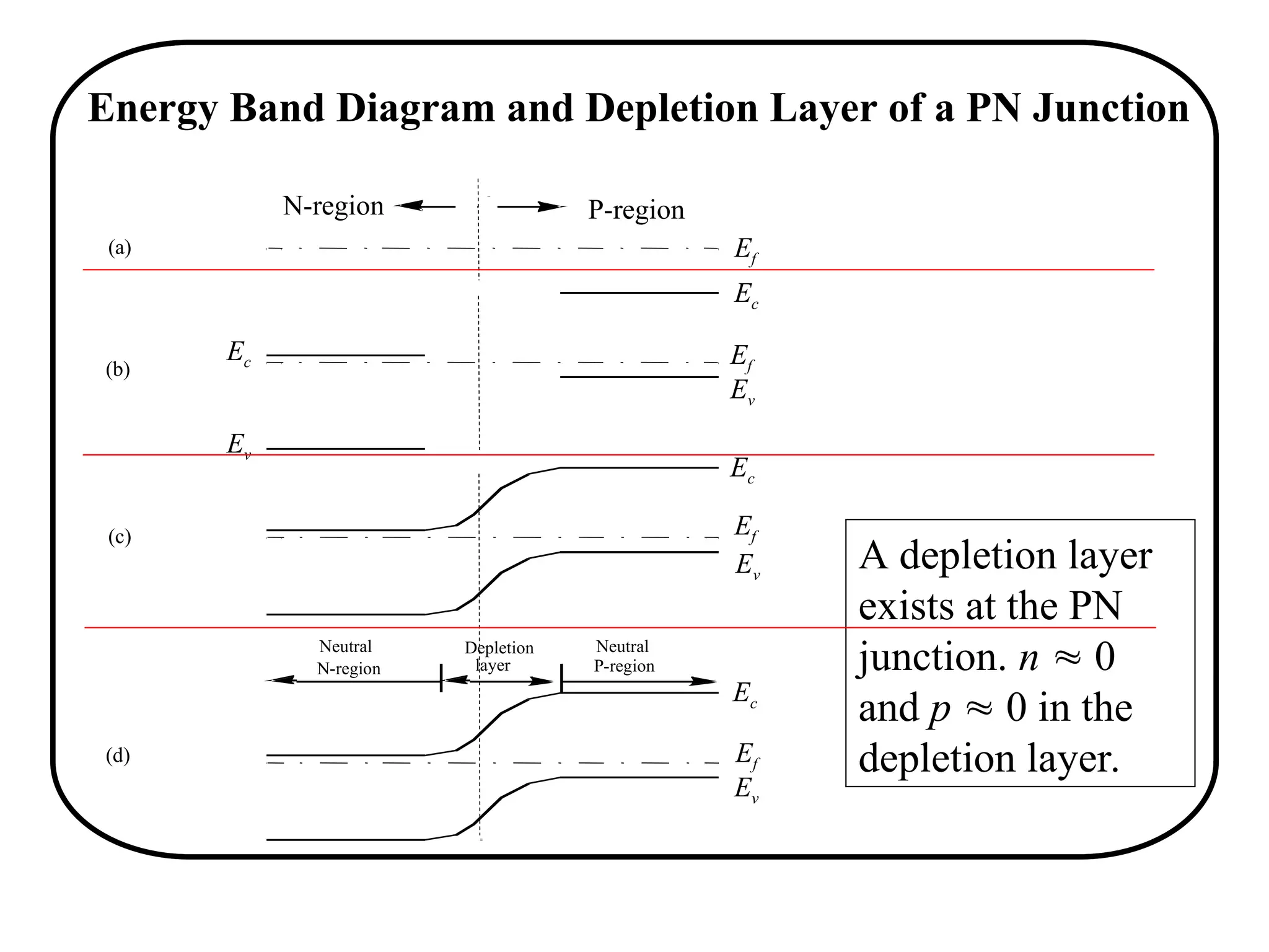
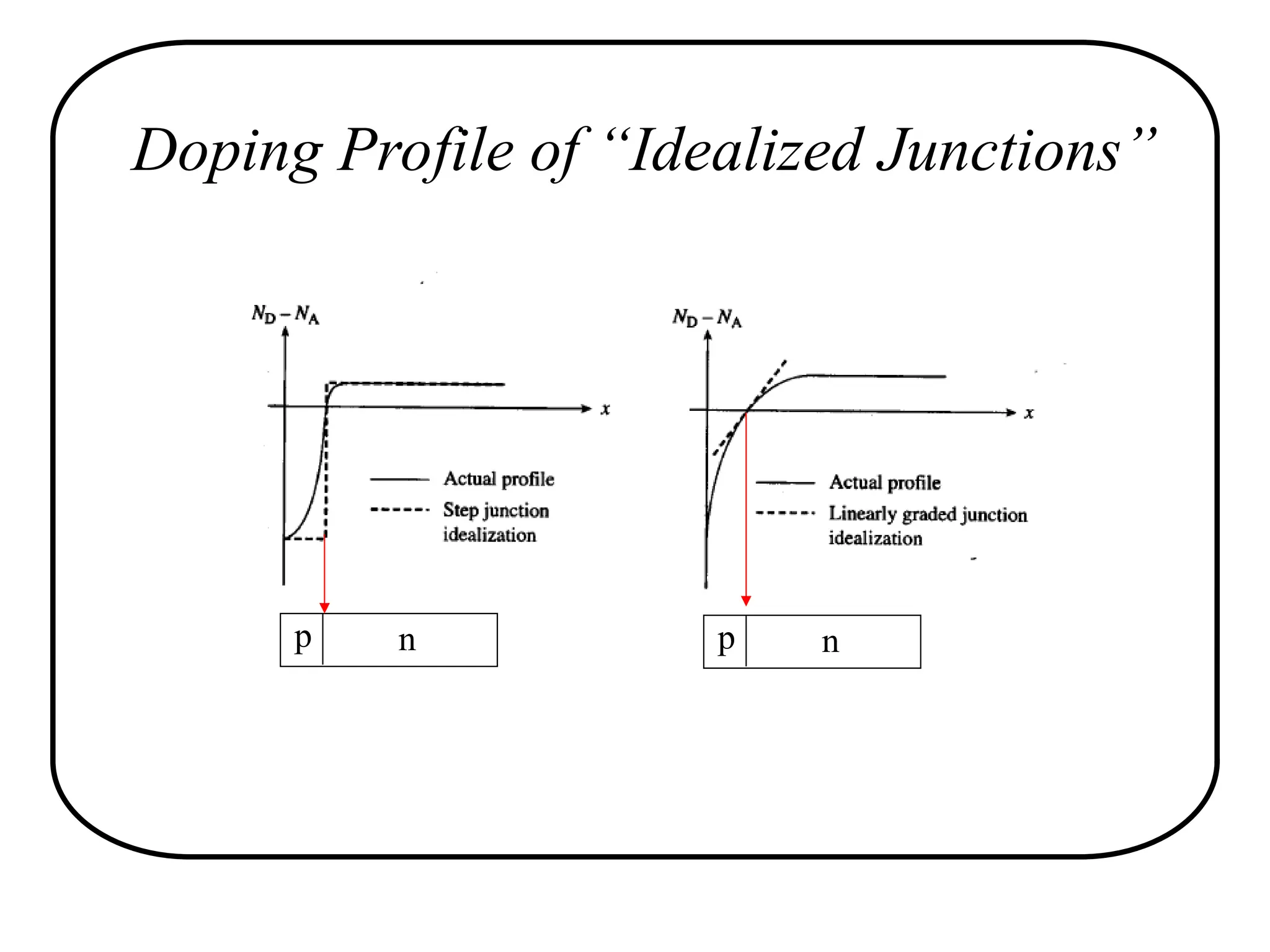
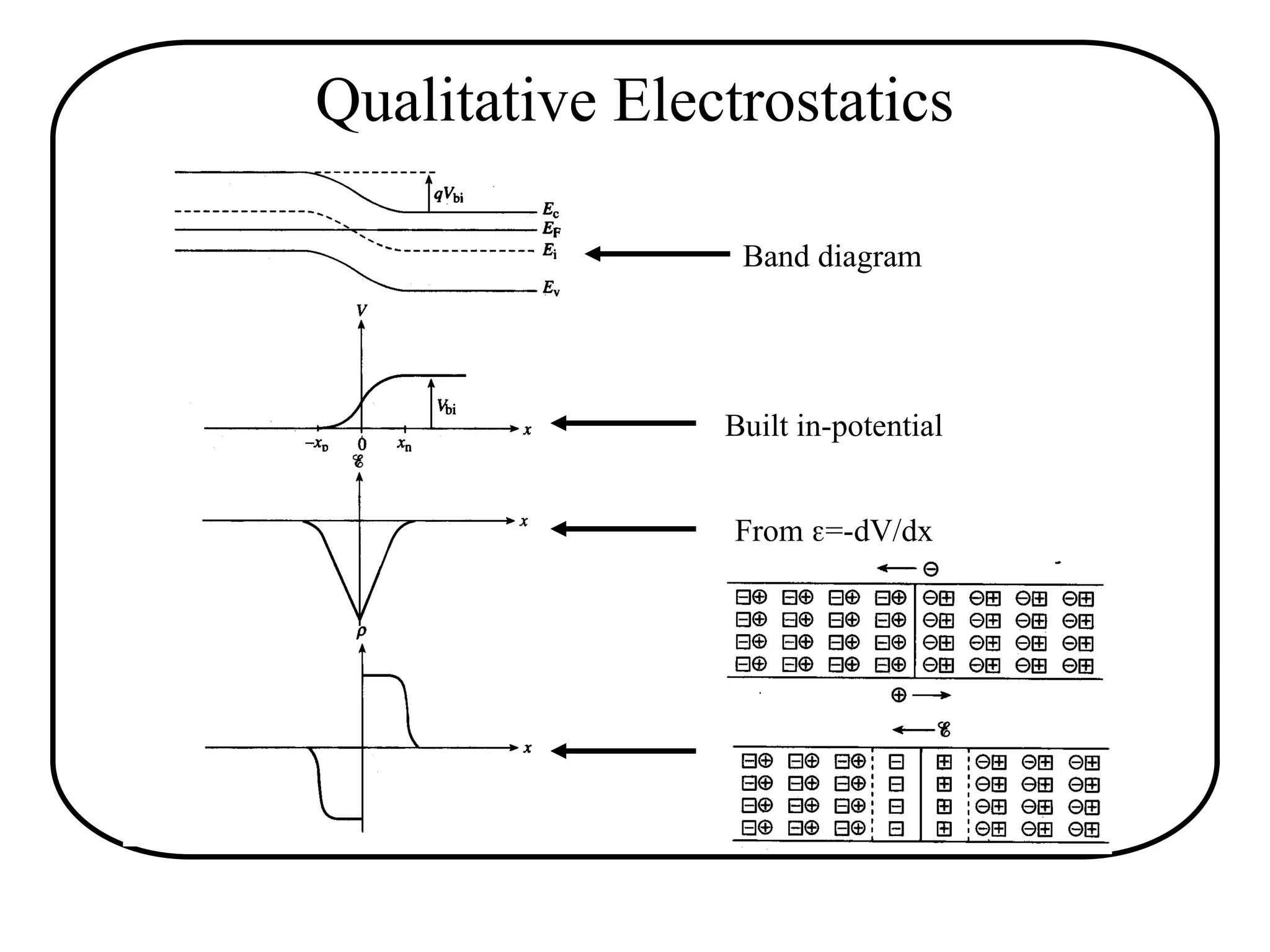
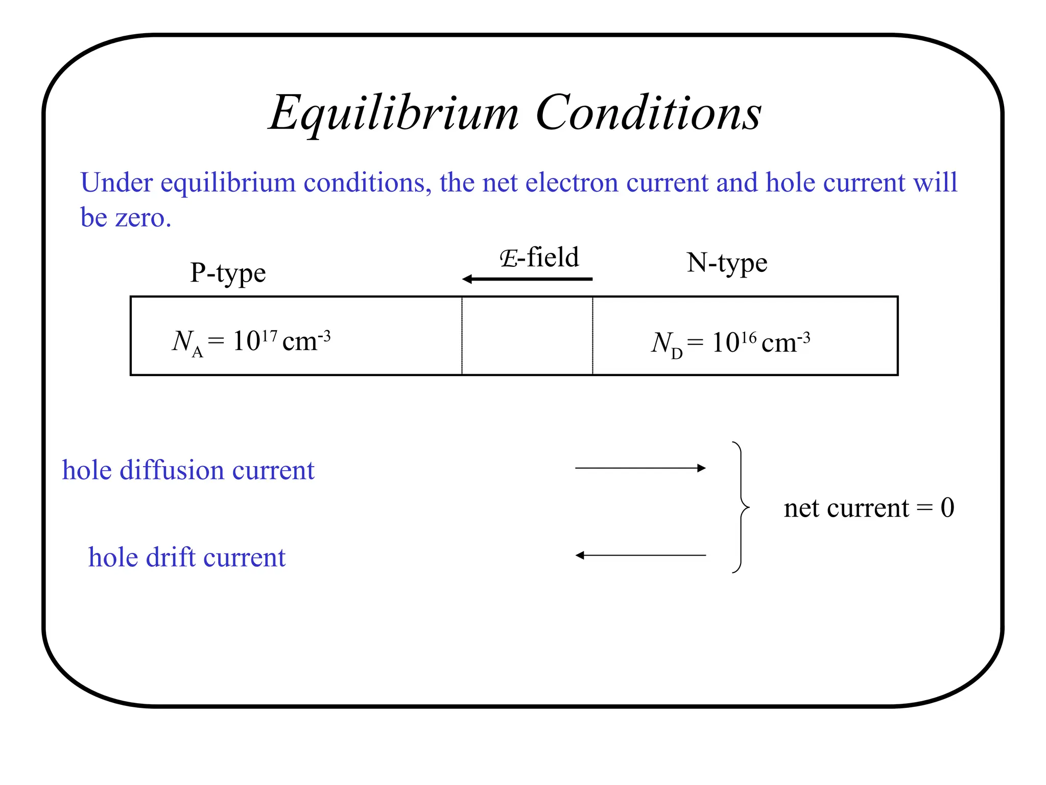
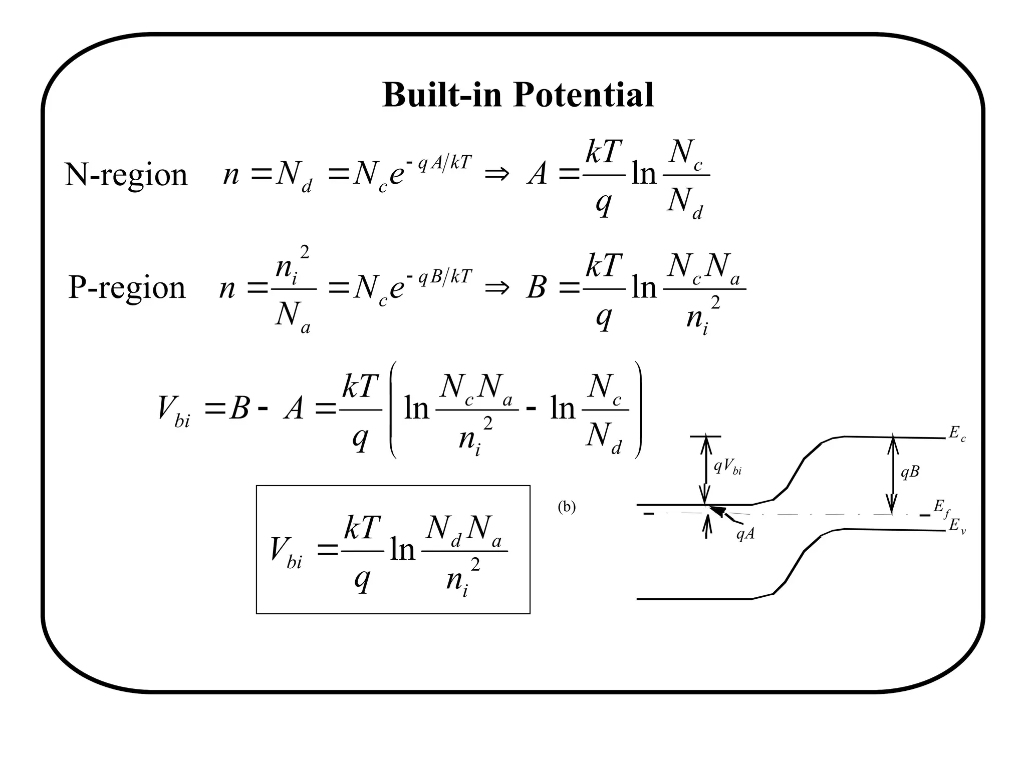
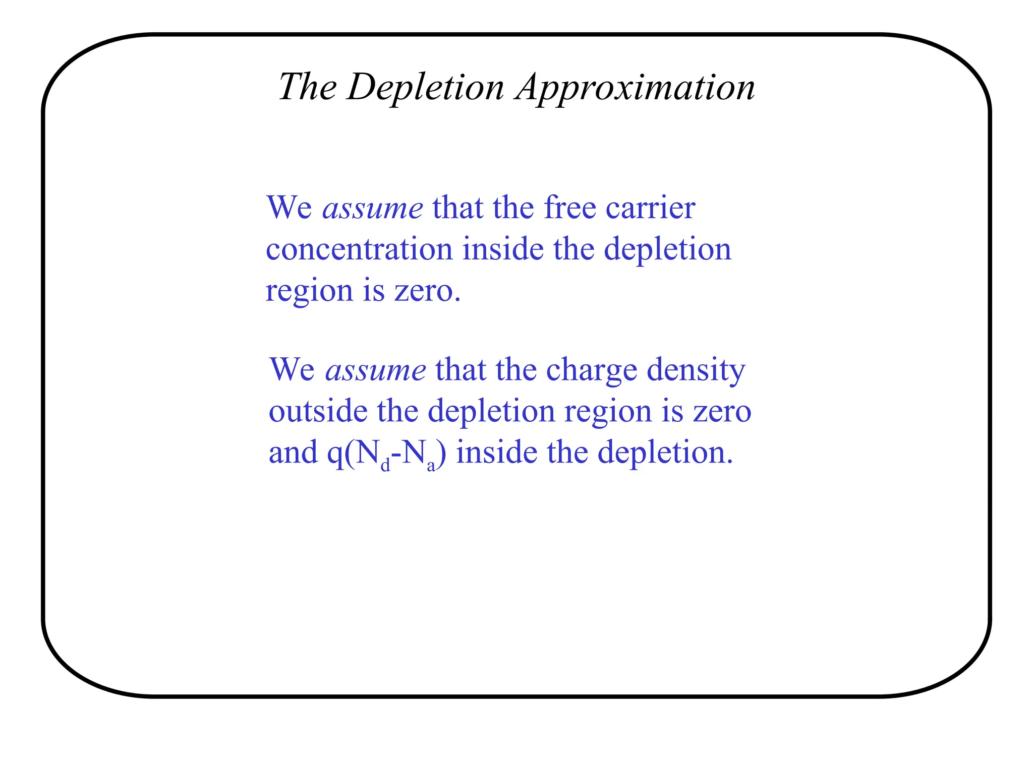
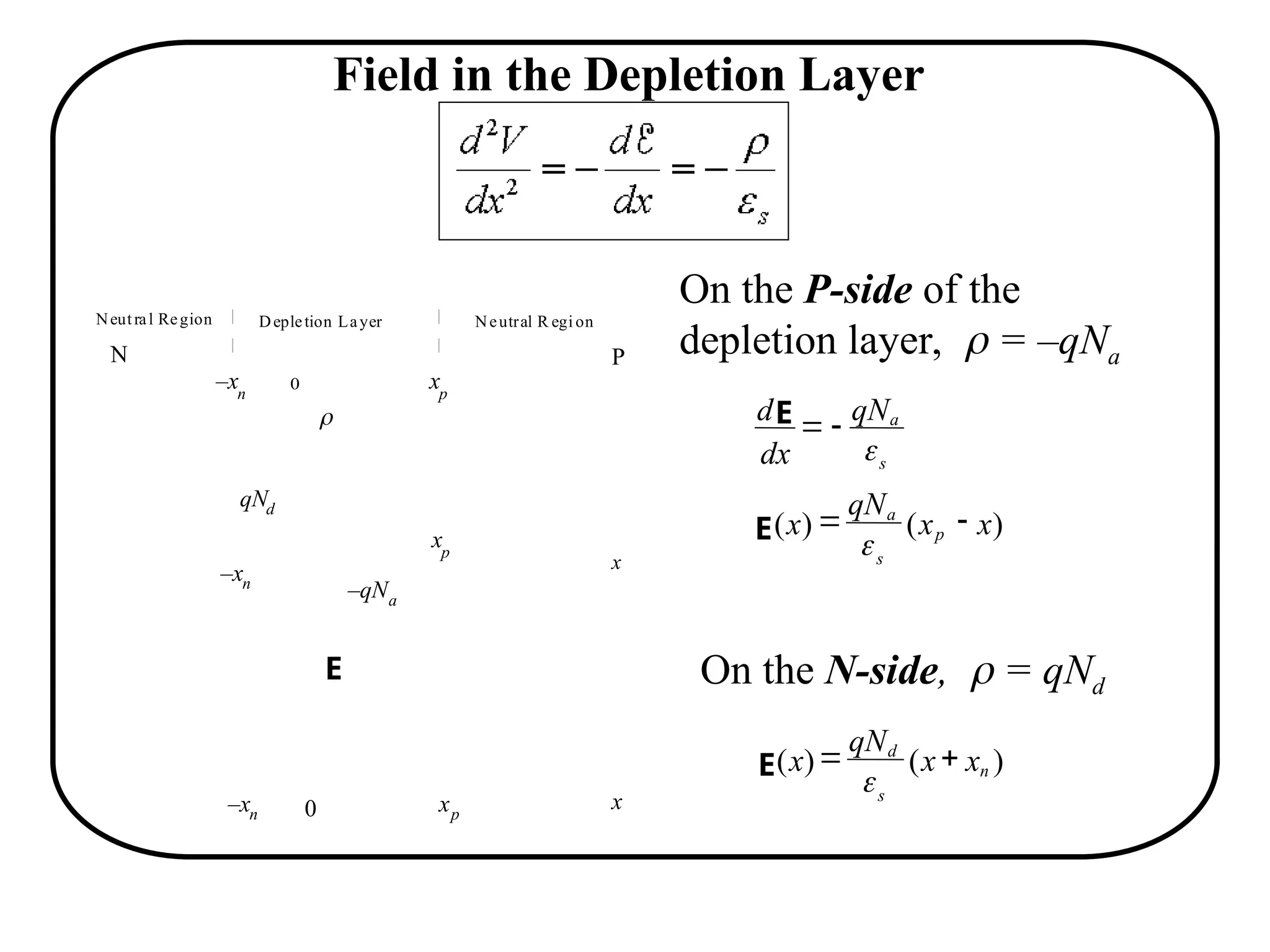
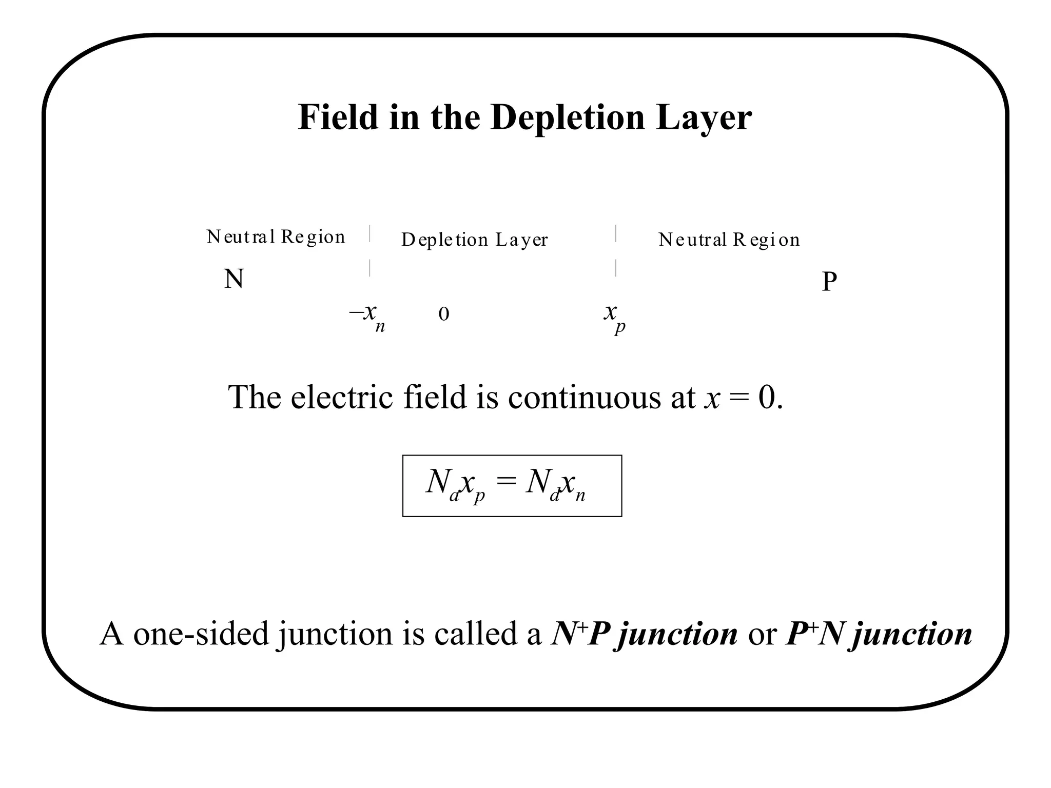
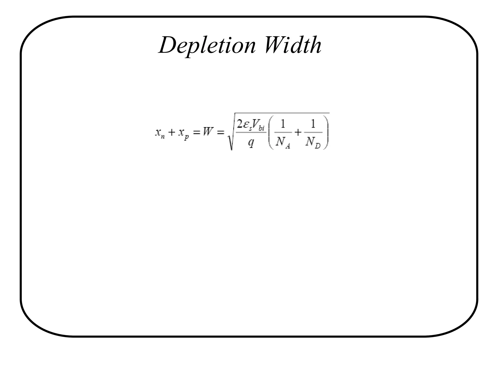
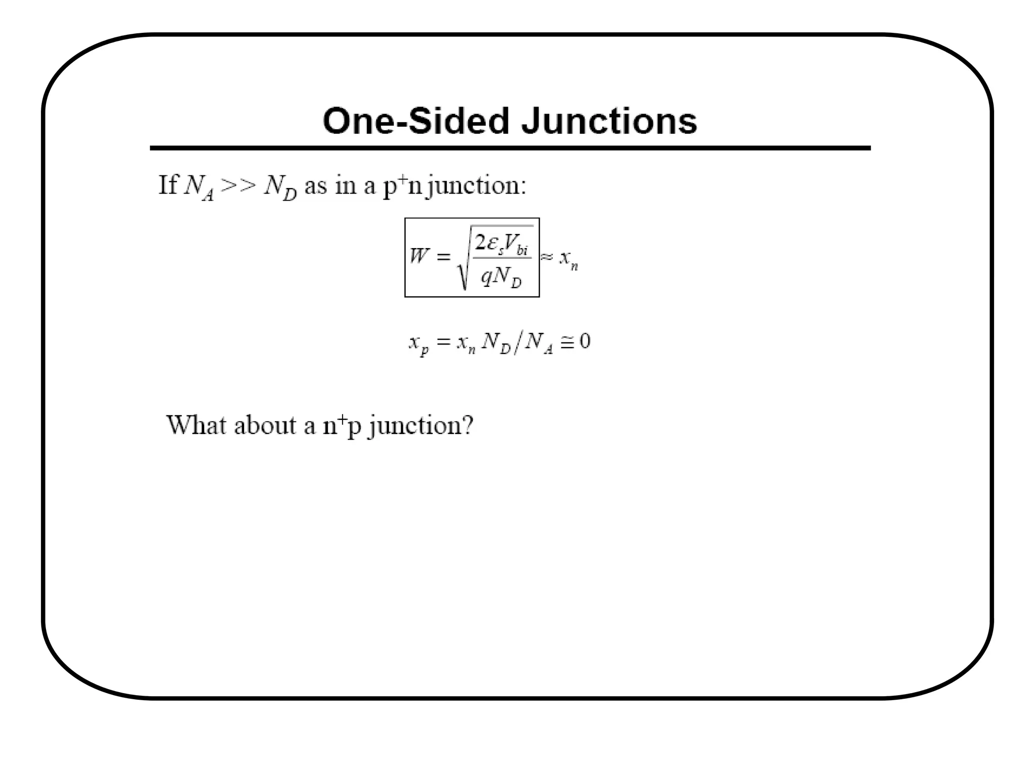
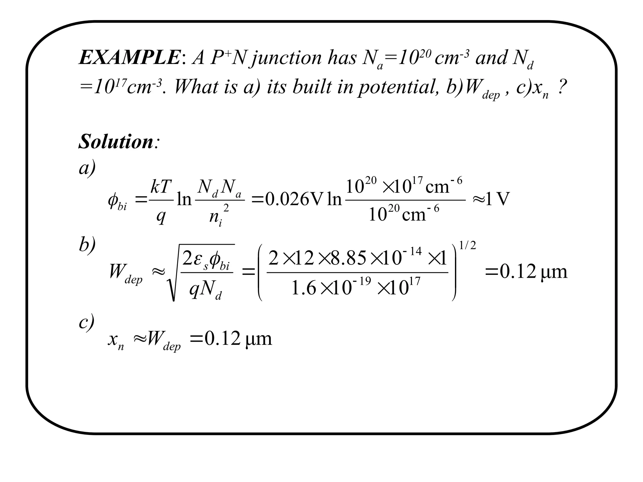
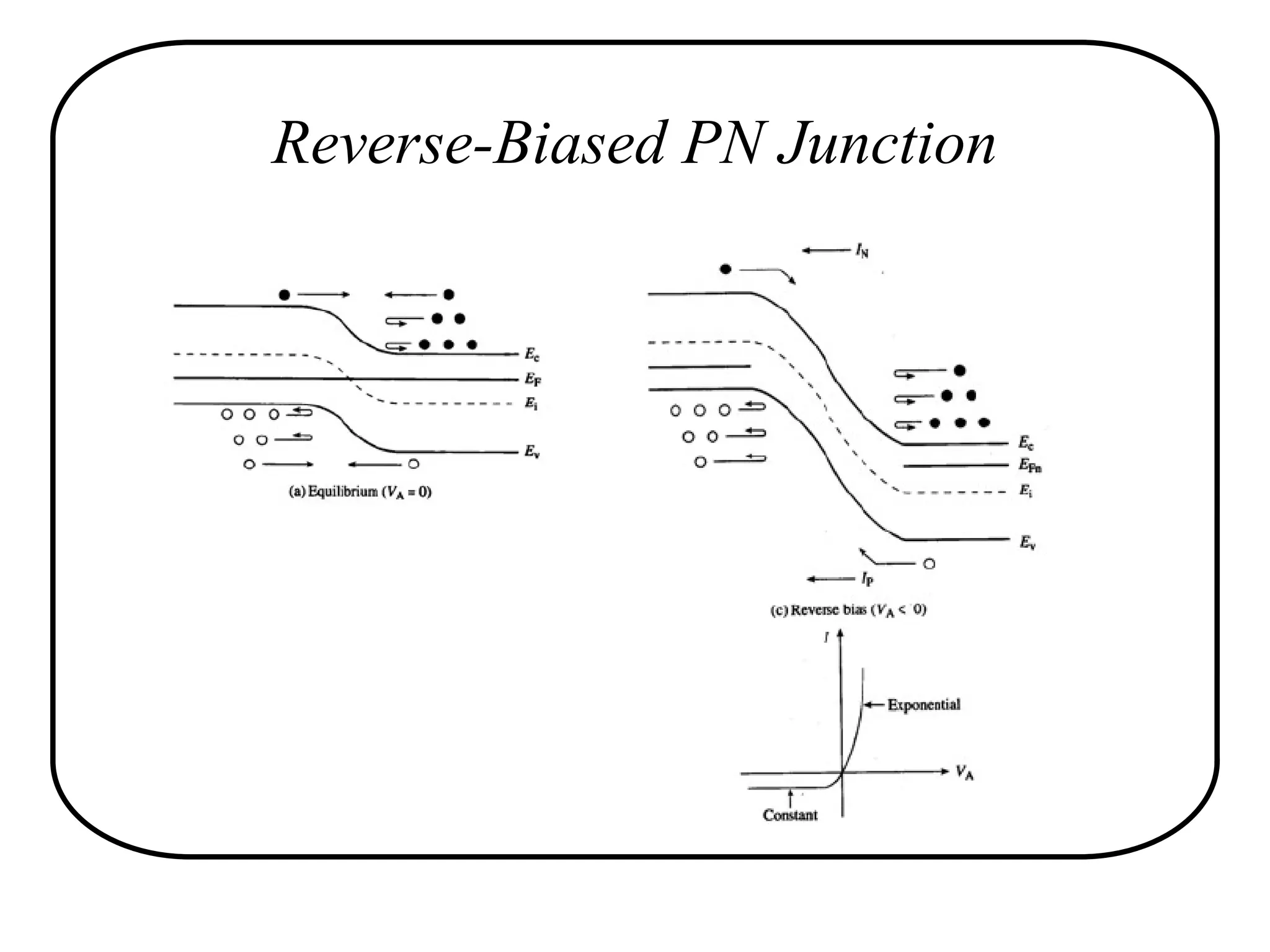
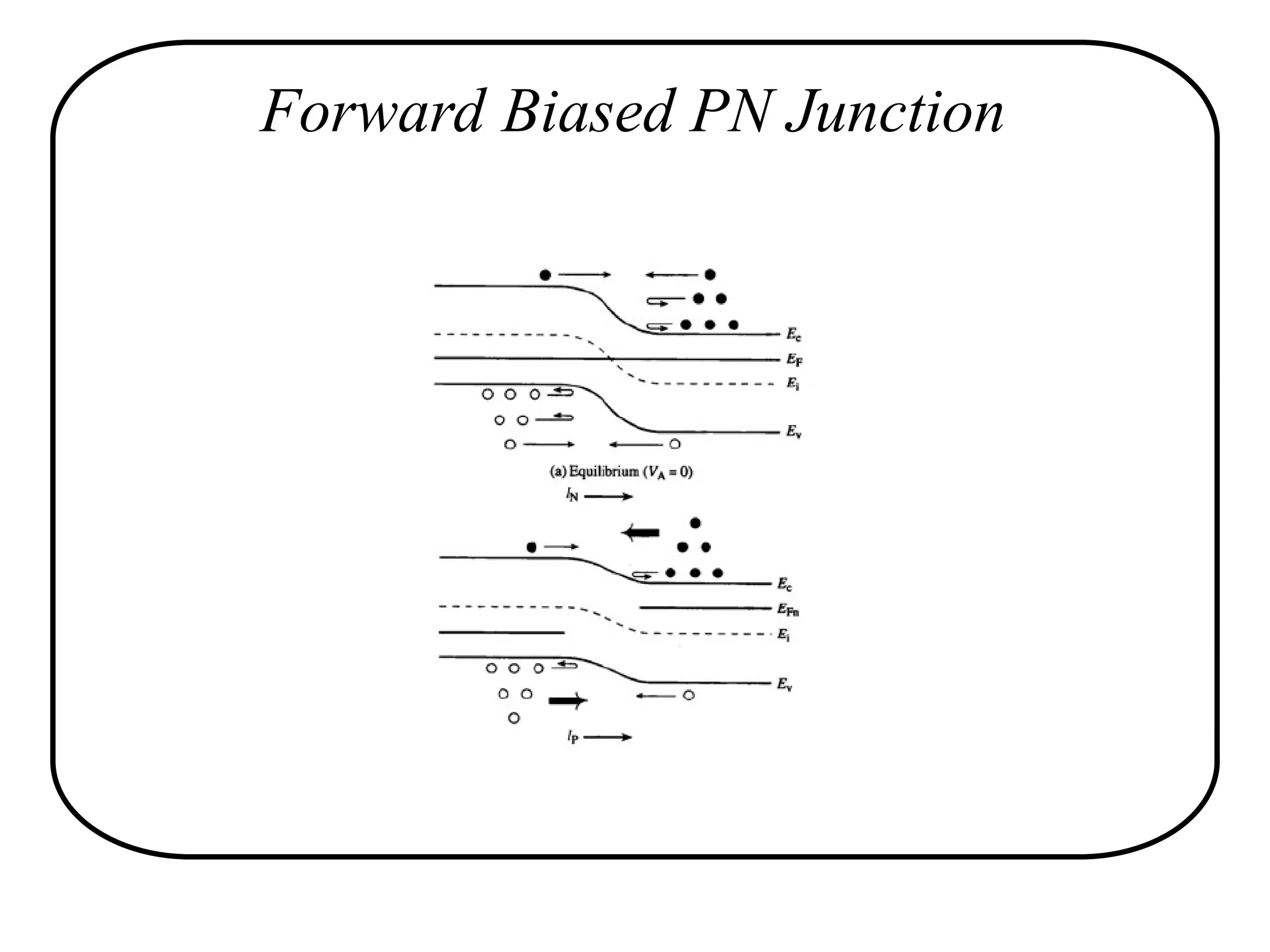
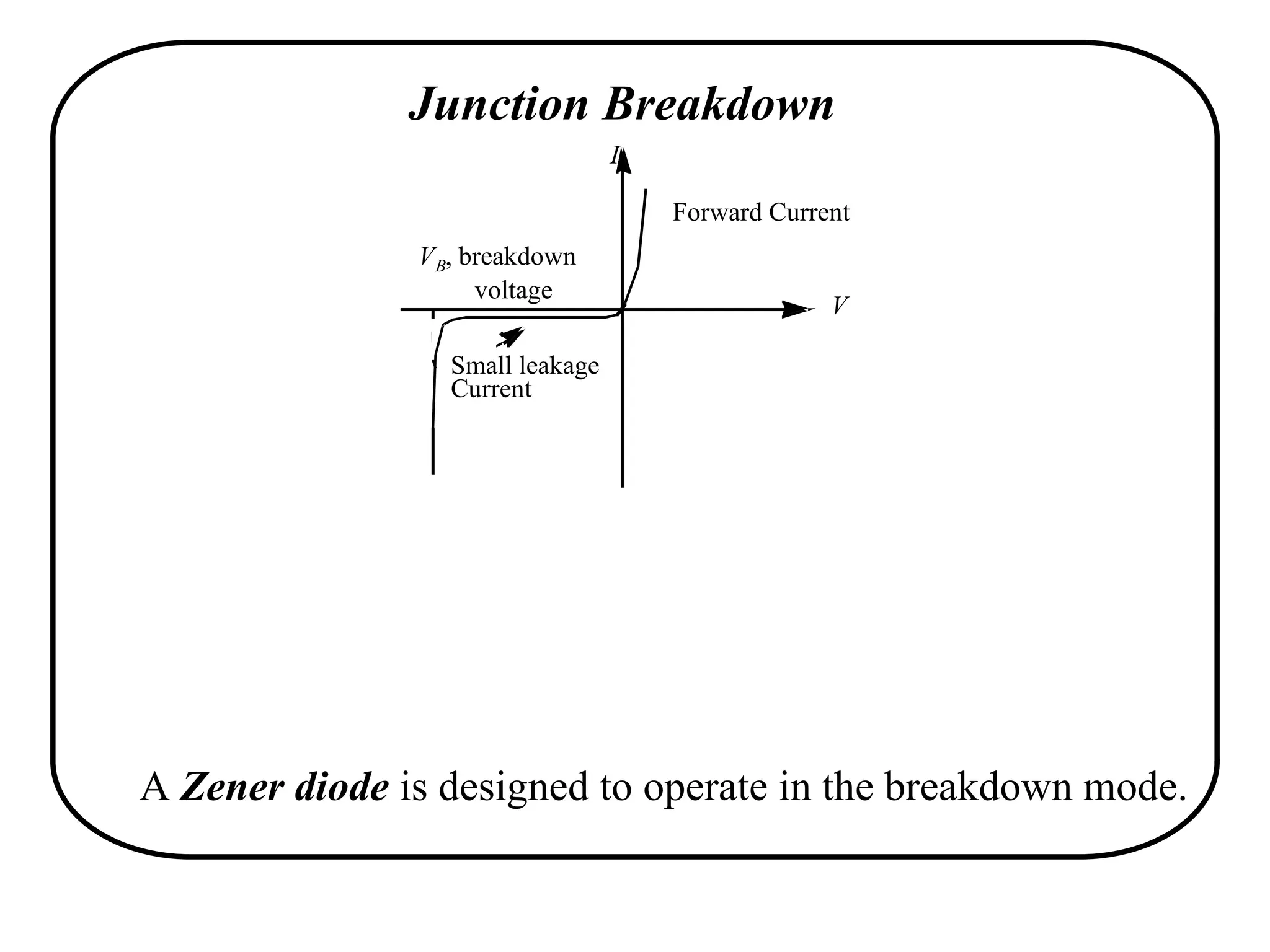
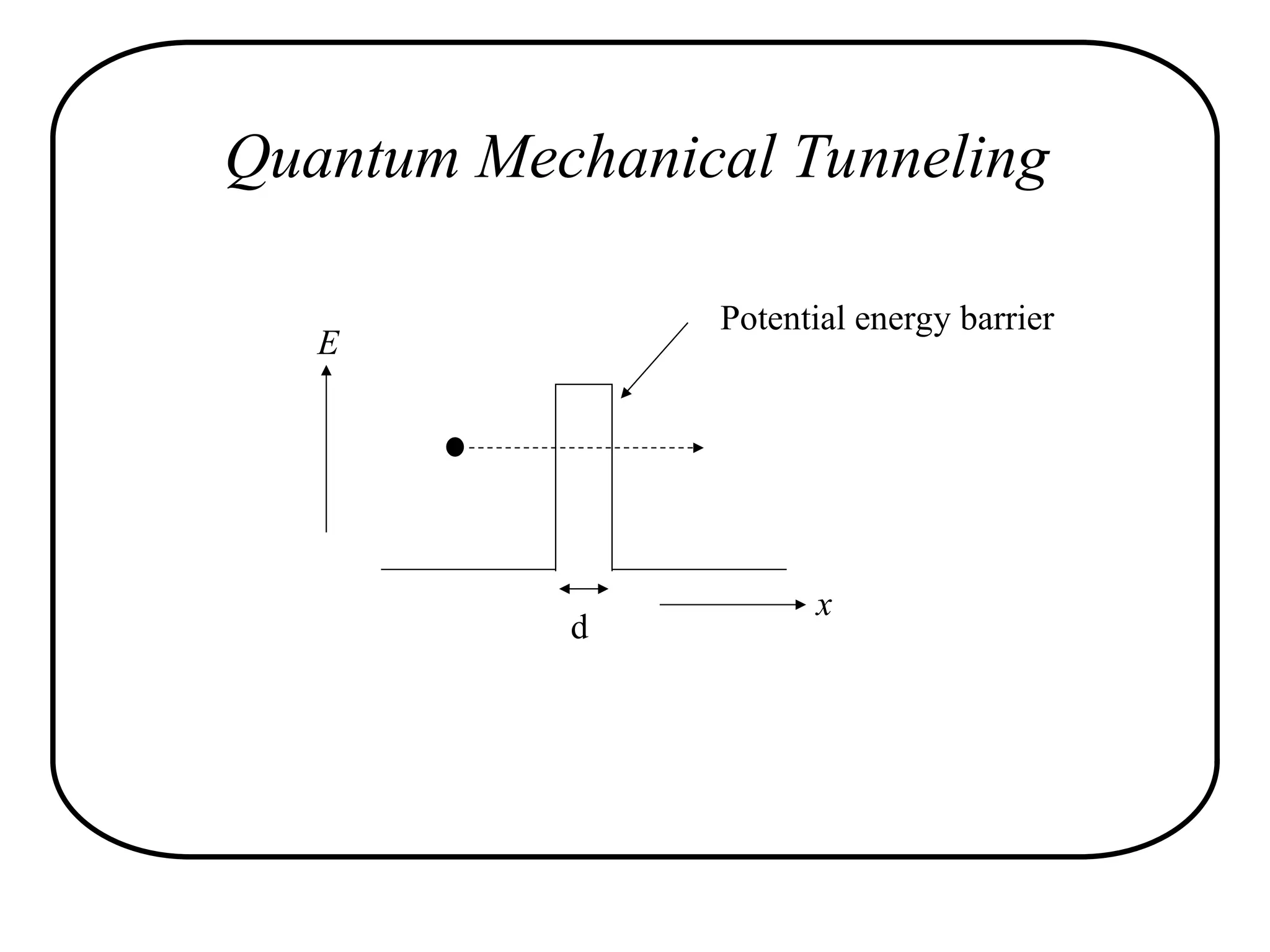
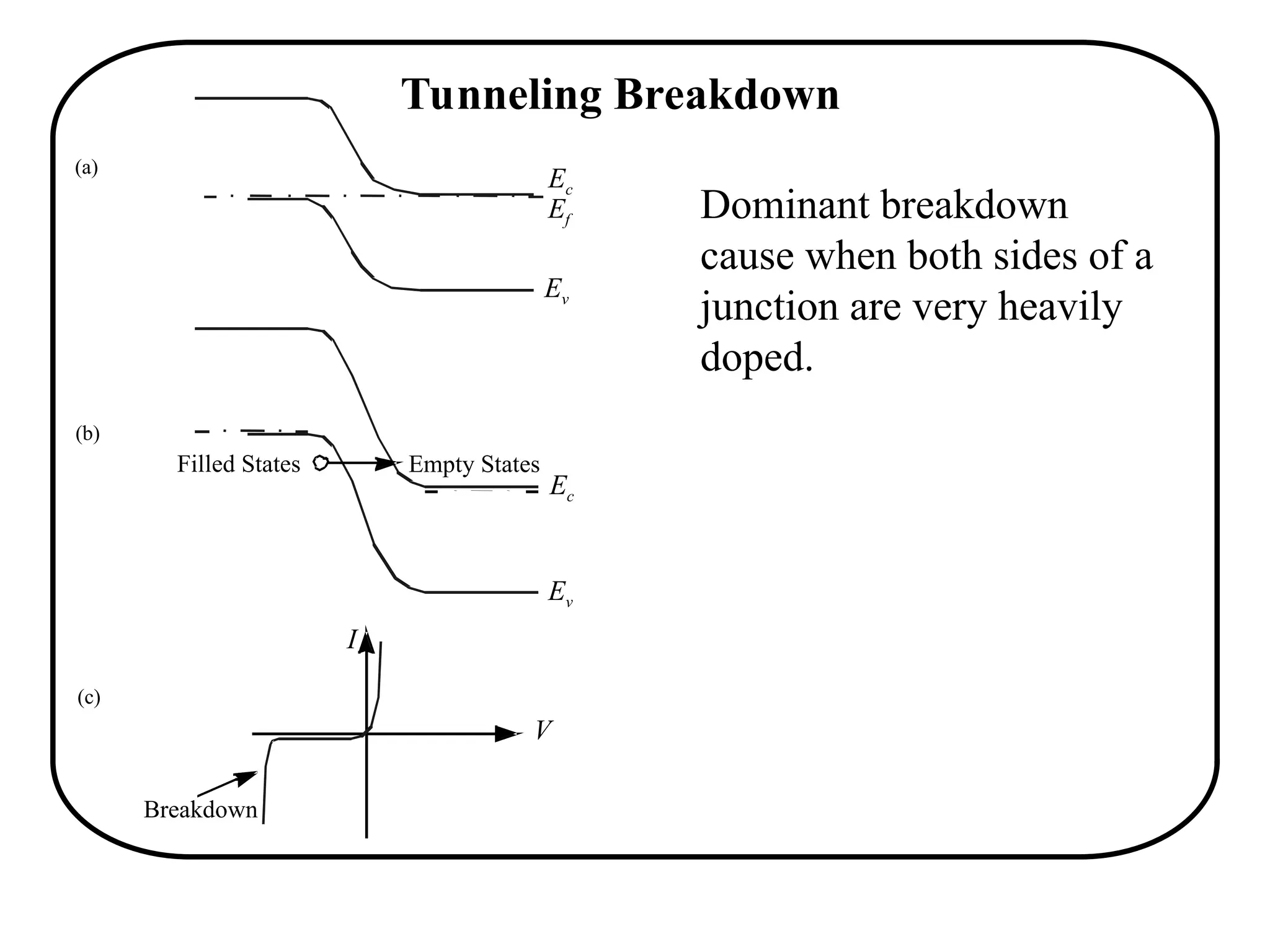
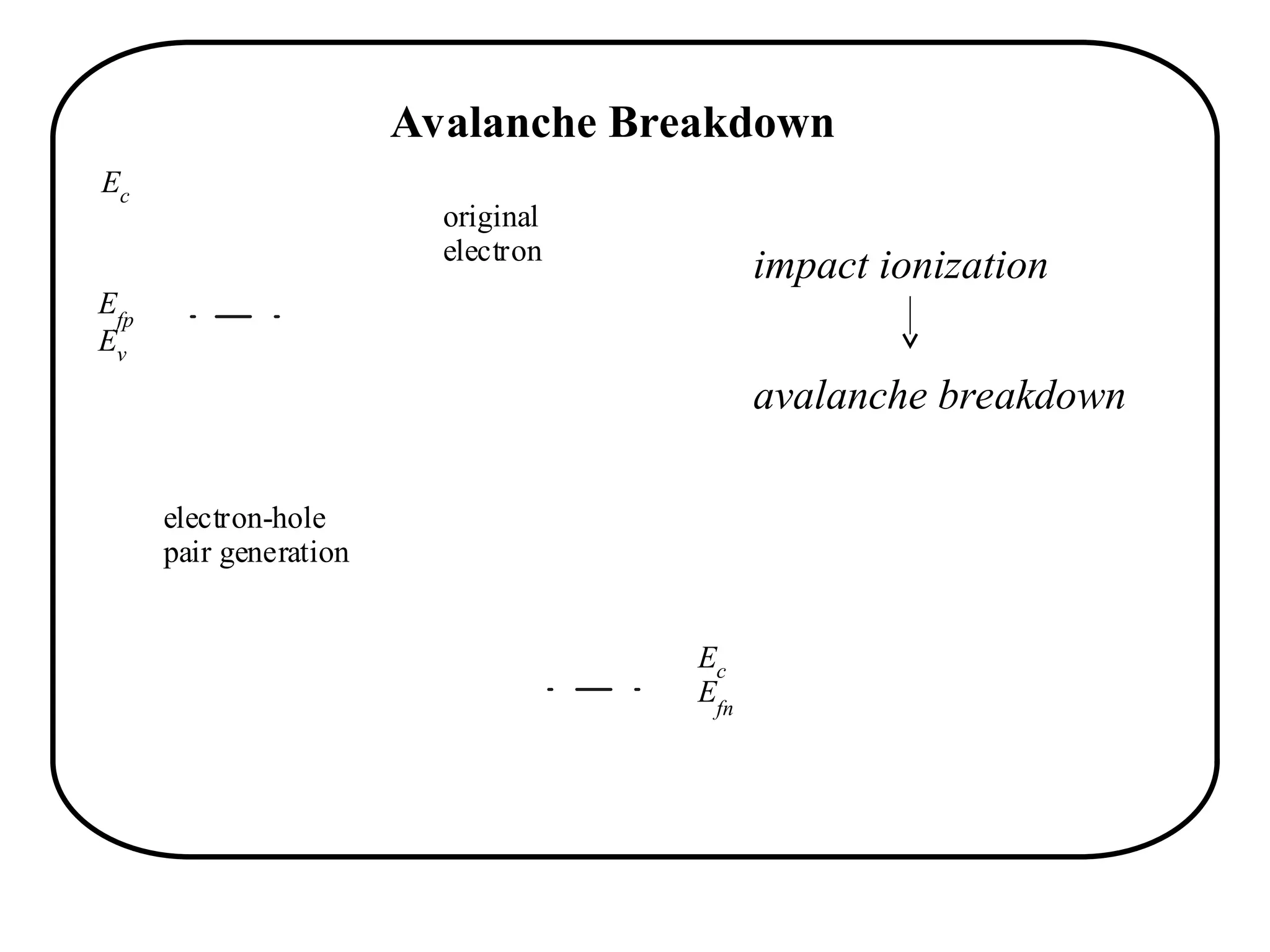
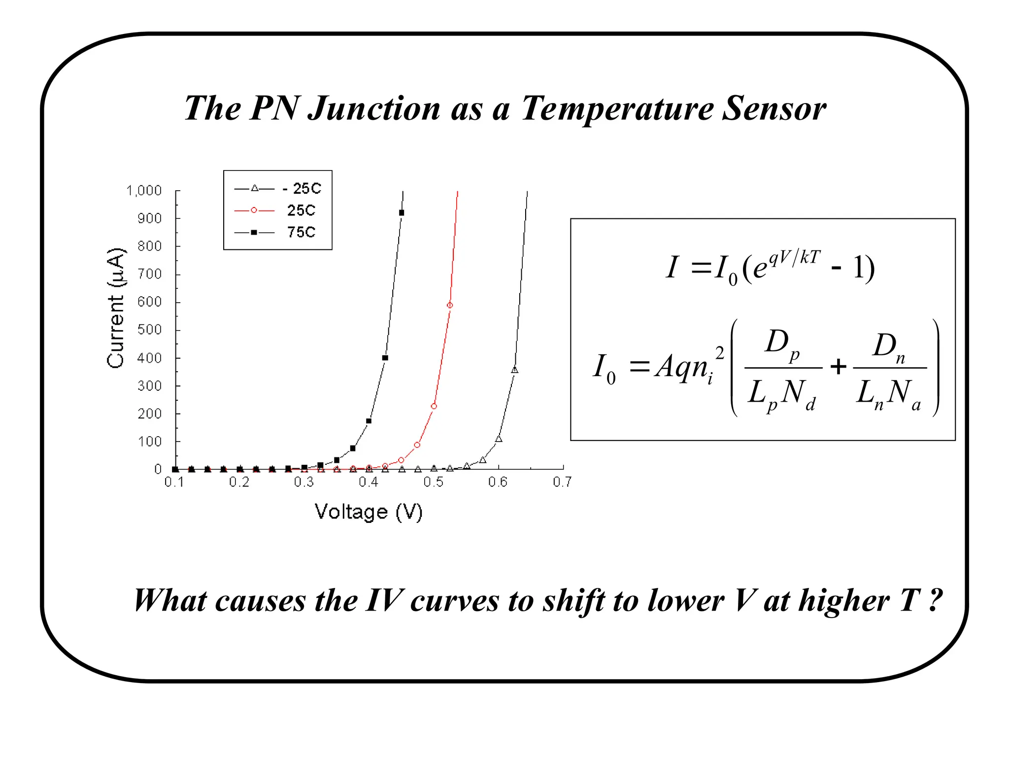
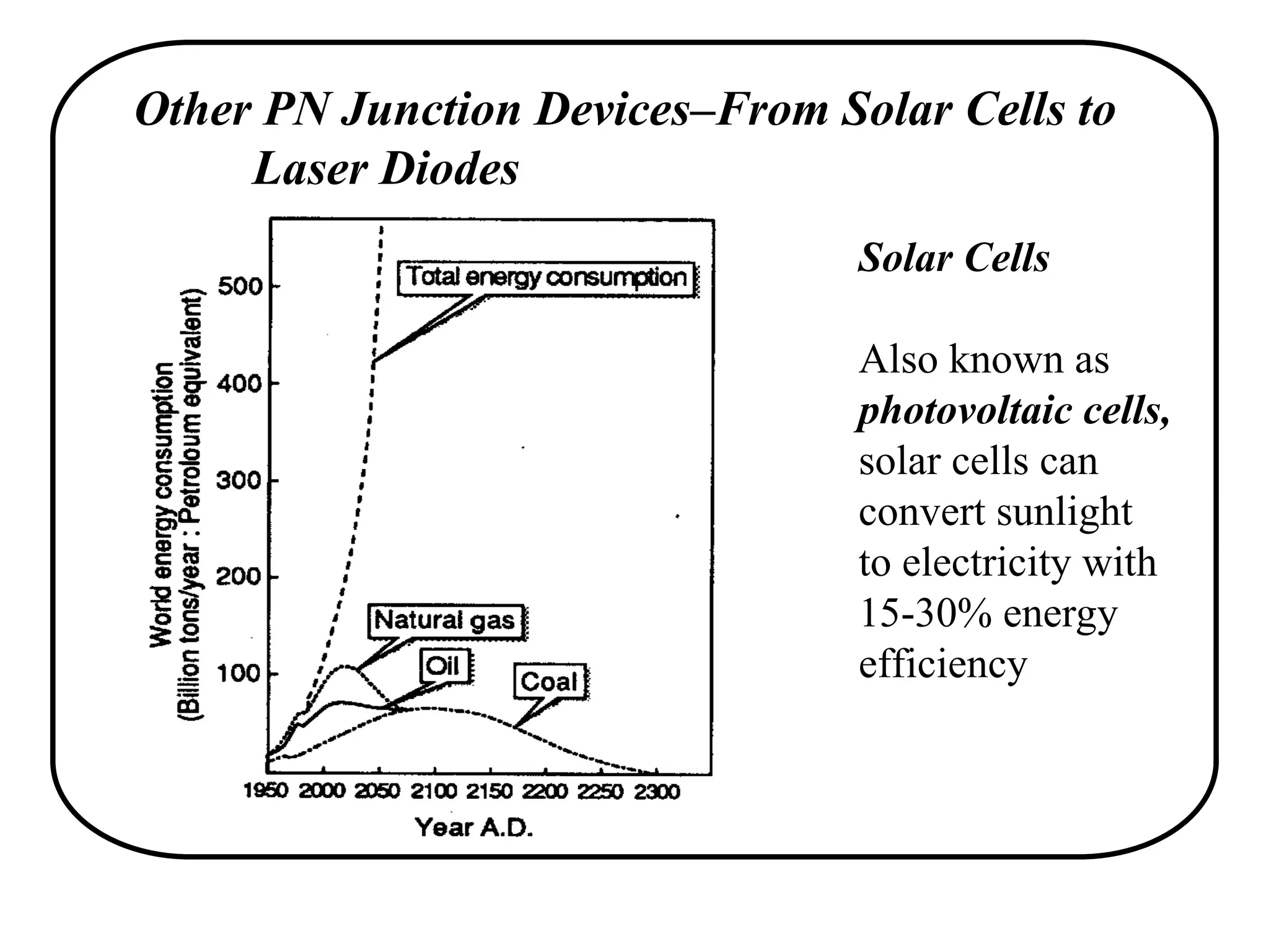
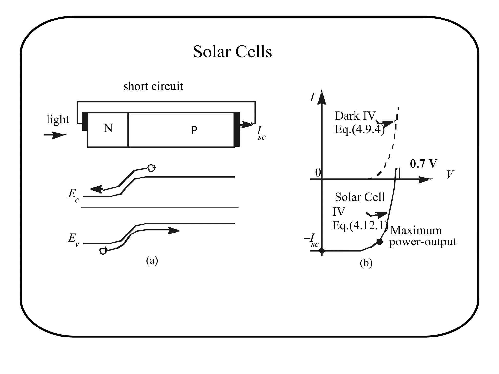
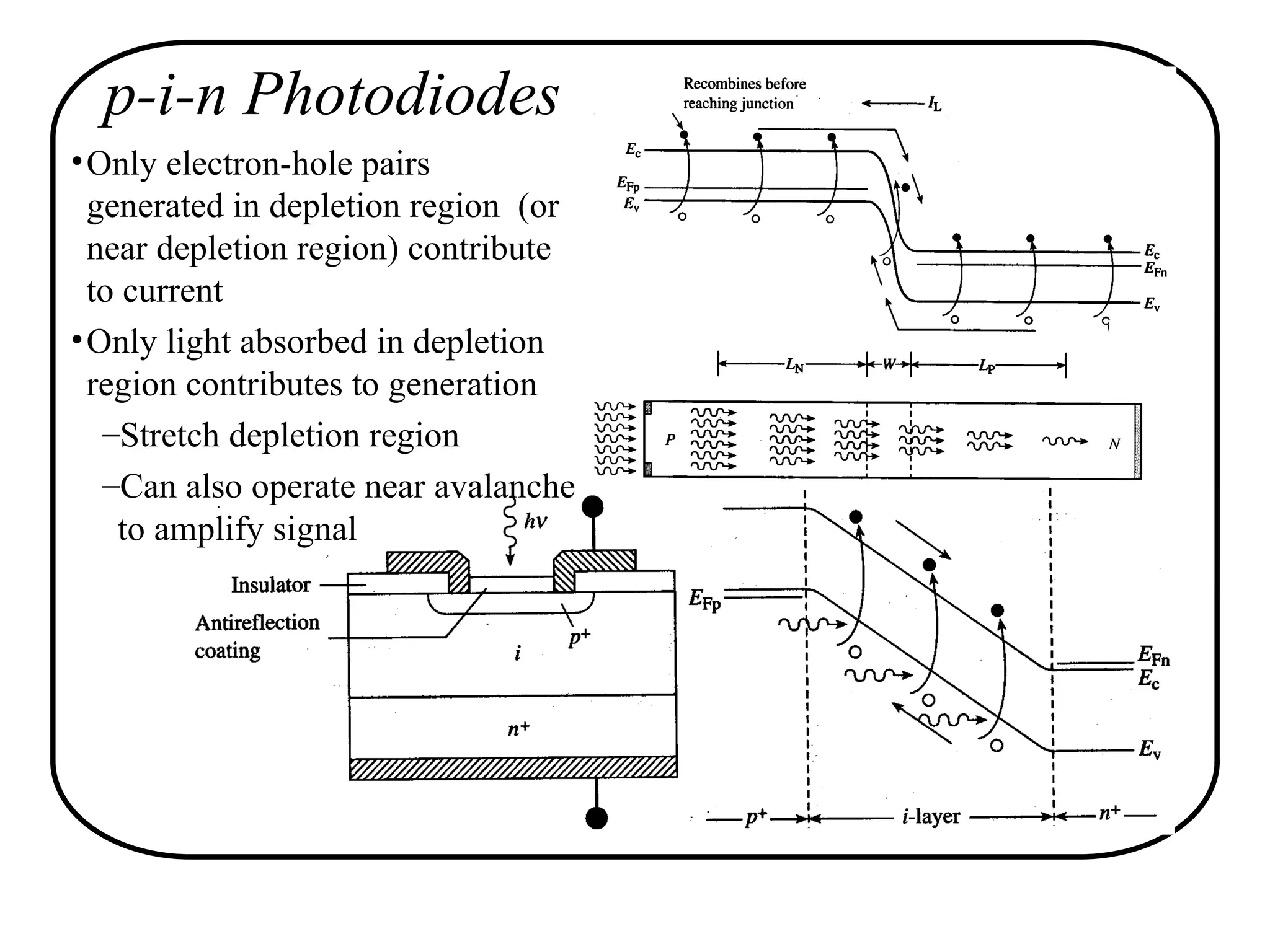
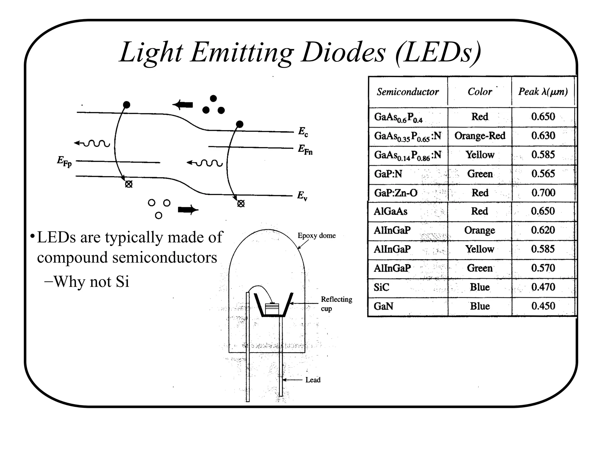
PHS 468: SEMICONDUCTOR
DEVICES
DR. O. D. AKINYEMI
DEPARTMENT OF PHYSICS,
UNIVERSITY OF AGRICULTURE,
ABEOKUTA, NIGERIA.
This lecture note was prepared using materials from lecture notes
prepared by Professor Ali Javey (Integrated Circuit Devices) and that of
Dr. K. Fobelets (An introduction to semiconductor devices)
Why study semiconductor devices?
Present day devices are no longer just diodes or transistors,
but are either large scale integrated circuits or special
purpose components whose design and performance are
intimately connected with their physics and processing.
For the future engineer it is no longer enough to study the
terminal electrical characteristics of the semiconductor
device while treating the device itself as a “black box”.
Most of the sophistication of modern electronics is hidden
in that box, and more and more engineering and scientific
effort will be required in device development, design,
simulation, production and testing in the future.
Why study semiconductor devices?
The devices in fact become subsystems, ready for use for
the system engineer. Even he, the user of the devices, will
not be able to get the most out of them or contribute
towards design of more advanced devices and systems
without a good knowledge of the principles underlying
their operation and the technology used in
manufacturing them. This course therefore aims to give
you the basic knowledge to understand simple
semiconductor devices and to give you a background that
will enable you to understand more complicated structures.
The course aims
• To give insight into the structure of
semiconductors
• To give insight into the physics of semiconductor
diodes and transistors.
• To give models of device behaviour that can be
used as a basis for understanding the functioning
of other/new semiconductor devices.
• To give insight into the fabrication methods of
diodes and transistors.
Objectives
At the end of the course students should be able to:
• Discuss the characteristics of semiconductors, in particular
Si, that make the material suitable for electronic devices
• Explain qualitatively the mechanisms of electronic
conduction in semiconductors, and calculate relevant
quantities from given data.
• Calculate and explain the DC current-voltage behaviour of
diodes and transistors, given their geometry and material
properties.
• Explain the fabrication of simple diodes and transistors.
Course synopsis
1. Introduction into semiconductor materials
A semiconductor is a material with a conductivity level between metals and
insulators. Unlike metals, the charges in the semiconductor are more tightly
bound to the atoms and although some of these charges travel around
in the semiconductor, they are only quasi-free as they feel the
continuous influence of the surrounding lattice (atoms). Semiconductors’
strength is based on the existence of 2 types of moving charges: negatively
charged electrons and positively charged holes. The energetic state of the
charges is described using an “energy band model” which is based on sound
quantum-mechanical calculations but which will be introduced in a more
informal way in this course. The energy band diagram with its associated
bandgap and position of the Fermi level will form the basis of understanding
the operation of semiconductor devices.
Two different types of currents, drift and diffusion, can occur in a
semiconductor. Although these currents normally occur at the same time in
“real” devices, in this course we take the liberty to make approximations such
that only one of them will occur at any one time. The reasoning behind the
approximations is based on the concept of majority and minority carriers.
2. The MOS capacitor and MOSFET
Semiconductors become devices the moment they are combined with
other types of semiconductors or metals. A semiconductor with two
metal contacts becomes a resistor or a Schottky diode depending on
the material characteristics of both the semiconductor and the metal.
We will look into this kind of metal-semiconductor junctions.
Although in traditional textbooks it is common to start with discussing
the functioning of a pn-diode, in this course we will first focus on
what is called majority carrier devices - devices where only one type
of carriers play an important role in its operation. A metal-oxide-
semiconductor (MOS) contact can be used as a capacitor in integrated
circuits but is also used in MOS Field Effect Transistors (MOSFETs)
to control the conduction in the channel without injecting carriers. We
will study the functioning of this device using energy band diagrams
and investigate the parameters that influence the operation of this
device.
3. The p-n junction and BJT
Diodes can be made from pn junctions - thus the same material but
different doping types at each side. This is a device where both
majority and minority carriers play an important role. The current is
governed by diffusion of minority carriers rather than by drift of
majority carriers as was the case in the MOSFET. We will explore the
reason for the rectifying behaviour of these pn-diodes.
A more complicated npn or pnp junction is the basis for the bipolar
junction transistor (BJT). Based on our knowledge of pn junctions, the
functioning of a BJT will be described. We will find out how current
gain exist in this device and we will find out why BJTs are used in
high-speed analogue applications whilst MOSFETs govern the digital
world.
SEMICONDUCTORS
* Intrinsic (i.e. pure, undoped) semiconductors
have a small amount of free carriers at room
temperature and therefore have a very low
conductivity (e.g. diamond). The number of holes
and electrons are equal in an intrinsic
semiconductor as the free carriers are generated by
thermal energy and thus whilst and electron is
created a holes occurs simultaneously (electron-
hole pairs).
ni = pi
ni is the intrinsic number of electrons
pi is the intrinsic number of holes
* Extrinsic (i.e. doped) semiconductors have
better conductivity.
dopants + intrinsic = extrinsic
semiconductor semiconductor
• Impurities, donors or acceptors, are introduced in
the pure intrinsic semiconductor. Thermal energy
frees electrons from donor atoms, and holes from
acceptor atoms.
• Donor doping (donors donate an extra electron)
creates an n-type material. The donor density
notation is ND Acceptor doping creates a p-type
material. The acceptor density notation is NA
• The density of dopants is normally higher than the
intrinsic density of free carriers in the
semiconductor. (e.g. for Si ni=1.45x 10¹⁰
cm-3
whilst doping density introduced in the lattice is
>1015
cm-3
)
In semiconductors two types of current can
exist: drift and diffusion currents. It is the
aim of this section to generate an
understanding into the physical principles
behind the existence of the currents.
Drift currents
If an electric (or magnetic) field is applied
then the motion of the carriers is still under
the influence of scattering processes, and
each individual carrier might not take
necessarily the same path, but the average
direction of movement (velocity) of all the
carriers is determined by the applied
electric field. This motion of carriers under
an applied electric field is called drift.
Diffusion Currents
As seen before generation of carriers via temperature is always in pairs
of electrons and holes and thus the number of
electrons and holes caused by generation is equal (the intrinsic carrier
concentration at a certain temperature). Assume
that a process exists that can create locally an excess of one type of
carriers compared to the other. This would generate
a local gradient of carriers. The carriers are going to react as what you
would expect from gas molecules. If at a corner
of the room a chemical (e.g. gas molecules different than nitrogen and
oxygen that normally occur in air) the after a
while the observer can smell the gas at the other side of the room
because the molecules have diffuse throughout the
room to cancel the gradient in its density. The same happens with
excess carriers in a semiconductor, they will diffuse in
order to eliminate the excess. This diffusion is indeed not completely
random any more as it moves the carriers on
average in the direction determined by the gradient. This process will
cause diffusion currents.
PN Junctions
A PN junction is present in every semiconductor device.
N-type
P-type
Donors
V
I
Reverse bias Forward bias
N P
V
I
diode
symbol
– +
N-region P-region
(a)
(b)
(c)
(d)
Depletion
layer
Neutral
P-region
Neutral
N-region
Ef
Energy Band Diagram and Depletion Layer of a PN Junction
A depletion layer
exists at the PN
junction. n  0
and p  0 in the
depletion layer.
Ec
Ef
Ev
Ec
Ev
Ef
Ec
Ev
Ef
Ev
Ec
Doping Profile of “Idealized Junctions”
p n p n
Qualitative Electrostatics
Band diagram
Built in-potential
From =-dV/dx
When the junction is formed, electrons from the n-side and holes
from the p-side will diffuse leaving behind charged dopant atoms.
Remember that the dopant atoms cannot move! Electrons will
leave behind positively charged donor atoms and holes will leave
behind negatively charged acceptor atoms.
The net result is the build up of an electric field from the
positively charged atoms to the negatively charged atoms, i.e.,
from the n-side to p-side. When steady state condition is reached
after the formation of junction (how long this takes?) the net
electric field (or the built in potential) will prevent further diffusion
of electrons and holes. In other words, there will be drift and
diffusion currents such that net electron and hole currents will be
zero.
Formation of pn junctions
Equilibrium Conditions
Under equilibrium conditions, the net electron current and hole current will
be zero.
NA = 1017
cm3
ND = 1016
cm3
hole diffusion current
hole drift current
net current = 0
E-field
P-type N-type
2
ln
i
a
d
bi
n
N
N
q
kT
V 
Built-in Potential
d
c
kT
A
q
c
d
N
N
q
kT
A
e
N
N
n ln



 
2
2
ln
i
a
c
kT
B
q
c
a
i
n
N
N
q
kT
B
e
N
N
n
n 


 












d
c
i
a
c
bi
N
N
n
N
N
q
kT
A
B
V ln
ln 2
N-region
P-region
(b) Ef
Ec
Ev
qVbi qB
qA
The Depletion Approximation
We assume that the free carrier
concentration inside the depletion
region is zero.
We assume that the charge density
outside the depletion region is zero
and q(Nd-Na) inside the depletion.
On the P-side of the
depletion layer,  = –qNa
On the N-side,  = qNd
a)
N P
Nd
Na
Depletion Layer Neutral R egi on
–xn
0 xp
b)
x
xp
–xn
c)
qNd
–qNa
x

E
–xn xp

)
P
N
0

bi
)
Neutral Region
V
s
a
qN
dx
d



E
E
)
(
)
( x
x
qN
x p
s
a



E
)
(
)
( n
s
d
x
x
qN
x 


E
Field in the Depletion Layer
The electric field is continuous at x = 0.
Naxp = Ndxn
A one-sided junction is called a N+
P junction or P+
N junction
(a)
N P
Nd
Na
Depletion Layer Neutral R egi on
–xn
0 xp
(b)
x
xp
–xn
(c)
qNd
–qNa

E

(d)
P
N
Neutral Region
Depletion Width
EXAMPLE: A P+
N junction has Na=1020
cm-3
and Nd
=1017
cm-3
. What is a) its built in potential, b)Wdep , c)xn ?
Solution:
a)
b)
c)
V
1
cm
10
cm
10
10
ln
V
026
.
0
ln 6
20
6
17
20
2



 

i
a
d
bi
n
N
N
q
kT

μm
12
.
0
10
10
6
.
1
1
10
85
.
8
12
2
2
2
/
1
17
19
14
















 

d
bi
s
dep
qN
W


μm
12
.
0

 dep
n W
x
Reverse-Biased PN Junction
Forward Biased PN Junction
Junction Breakdown
A Zener diode is designed to operate in the breakdown mode.
V
I
VB, breakdown
Forward Current
Small leakage
Current
voltage
Quantum Mechanical Tunneling
Potential energy barrier
d
E
x
Tunneling Breakdown
Dominant breakdown
cause when both sides of a
junction are very heavily
doped.
(a)
(b)
Empty States
Filled States
V
I
(c)
Breakdown
-
Ev
Ec
Ev
Ec
Ef
Avalanche Breakdown
impact ionization
avalanche breakdown
Ec
Efn
Ec
Ev
Efp
original
electron
electron-hole
pair generation
The PN Junction as a Temperature Sensor
What causes the IV curves to shift to lower V at higher T ?
)
1
(
0 
 kT
V
q
e
I
I










a
n
n
d
p
p
i
N
L
D
N
L
D
Aqn
I
2
0
Other PN Junction Devices–From Solar Cells to
Laser Diodes
Solar Cells
Also known as
photovoltaic cells,
solar cells can
convert sunlight
to electricity with
15-30% energy
efficiency
Solar Cells
N P
-
+
short circuit
light
I
sc
(a)
V
0.7 V
–I
sc
Maximum
power-output
Solar Cell
IV
I
Dark IV
0
(b)
Ec
Ev
Eq.(4.9.4)
Eq.(4.12.1)
p-i-n Photodiodes
•Only electron-hole pairs
generated in depletion region (or
near depletion region) contribute
to current
•Only light absorbed in depletion
region contributes to generation
–Stretch depletion region
–Can also operate near avalanche
to amplify signal
Light Emitting Diodes (LEDs)
•LEDs are typically made of
compound semiconductors
–Why not Si

electronic DEVICES and its basic theory.ppt

  • 1.
    PHS 468: SEMICONDUCTOR DEVICES DR.O. D. AKINYEMI DEPARTMENT OF PHYSICS, UNIVERSITY OF AGRICULTURE, ABEOKUTA, NIGERIA.
  • 2.
    This lecture notewas prepared using materials from lecture notes prepared by Professor Ali Javey (Integrated Circuit Devices) and that of Dr. K. Fobelets (An introduction to semiconductor devices)
  • 3.
    Why study semiconductordevices? Present day devices are no longer just diodes or transistors, but are either large scale integrated circuits or special purpose components whose design and performance are intimately connected with their physics and processing. For the future engineer it is no longer enough to study the terminal electrical characteristics of the semiconductor device while treating the device itself as a “black box”. Most of the sophistication of modern electronics is hidden in that box, and more and more engineering and scientific effort will be required in device development, design, simulation, production and testing in the future.
  • 4.
    Why study semiconductordevices? The devices in fact become subsystems, ready for use for the system engineer. Even he, the user of the devices, will not be able to get the most out of them or contribute towards design of more advanced devices and systems without a good knowledge of the principles underlying their operation and the technology used in manufacturing them. This course therefore aims to give you the basic knowledge to understand simple semiconductor devices and to give you a background that will enable you to understand more complicated structures.
  • 5.
    The course aims •To give insight into the structure of semiconductors • To give insight into the physics of semiconductor diodes and transistors. • To give models of device behaviour that can be used as a basis for understanding the functioning of other/new semiconductor devices. • To give insight into the fabrication methods of diodes and transistors.
  • 6.
    Objectives At the endof the course students should be able to: • Discuss the characteristics of semiconductors, in particular Si, that make the material suitable for electronic devices • Explain qualitatively the mechanisms of electronic conduction in semiconductors, and calculate relevant quantities from given data. • Calculate and explain the DC current-voltage behaviour of diodes and transistors, given their geometry and material properties. • Explain the fabrication of simple diodes and transistors.
  • 7.
    Course synopsis 1. Introductioninto semiconductor materials A semiconductor is a material with a conductivity level between metals and insulators. Unlike metals, the charges in the semiconductor are more tightly bound to the atoms and although some of these charges travel around in the semiconductor, they are only quasi-free as they feel the continuous influence of the surrounding lattice (atoms). Semiconductors’ strength is based on the existence of 2 types of moving charges: negatively charged electrons and positively charged holes. The energetic state of the charges is described using an “energy band model” which is based on sound quantum-mechanical calculations but which will be introduced in a more informal way in this course. The energy band diagram with its associated bandgap and position of the Fermi level will form the basis of understanding the operation of semiconductor devices. Two different types of currents, drift and diffusion, can occur in a semiconductor. Although these currents normally occur at the same time in “real” devices, in this course we take the liberty to make approximations such that only one of them will occur at any one time. The reasoning behind the approximations is based on the concept of majority and minority carriers.
  • 8.
    2. The MOScapacitor and MOSFET Semiconductors become devices the moment they are combined with other types of semiconductors or metals. A semiconductor with two metal contacts becomes a resistor or a Schottky diode depending on the material characteristics of both the semiconductor and the metal. We will look into this kind of metal-semiconductor junctions. Although in traditional textbooks it is common to start with discussing the functioning of a pn-diode, in this course we will first focus on what is called majority carrier devices - devices where only one type of carriers play an important role in its operation. A metal-oxide- semiconductor (MOS) contact can be used as a capacitor in integrated circuits but is also used in MOS Field Effect Transistors (MOSFETs) to control the conduction in the channel without injecting carriers. We will study the functioning of this device using energy band diagrams and investigate the parameters that influence the operation of this device.
  • 9.
    3. The p-njunction and BJT Diodes can be made from pn junctions - thus the same material but different doping types at each side. This is a device where both majority and minority carriers play an important role. The current is governed by diffusion of minority carriers rather than by drift of majority carriers as was the case in the MOSFET. We will explore the reason for the rectifying behaviour of these pn-diodes. A more complicated npn or pnp junction is the basis for the bipolar junction transistor (BJT). Based on our knowledge of pn junctions, the functioning of a BJT will be described. We will find out how current gain exist in this device and we will find out why BJTs are used in high-speed analogue applications whilst MOSFETs govern the digital world.
  • 10.
    SEMICONDUCTORS * Intrinsic (i.e.pure, undoped) semiconductors have a small amount of free carriers at room temperature and therefore have a very low conductivity (e.g. diamond). The number of holes and electrons are equal in an intrinsic semiconductor as the free carriers are generated by thermal energy and thus whilst and electron is created a holes occurs simultaneously (electron- hole pairs).
  • 11.
    ni = pi niis the intrinsic number of electrons pi is the intrinsic number of holes * Extrinsic (i.e. doped) semiconductors have better conductivity. dopants + intrinsic = extrinsic semiconductor semiconductor
  • 12.
    • Impurities, donorsor acceptors, are introduced in the pure intrinsic semiconductor. Thermal energy frees electrons from donor atoms, and holes from acceptor atoms. • Donor doping (donors donate an extra electron) creates an n-type material. The donor density notation is ND Acceptor doping creates a p-type material. The acceptor density notation is NA • The density of dopants is normally higher than the intrinsic density of free carriers in the semiconductor. (e.g. for Si ni=1.45x 1010 cm-3 whilst doping density introduced in the lattice is >1015 cm-3 )
  • 13.
    In semiconductors twotypes of current can exist: drift and diffusion currents. It is the aim of this section to generate an understanding into the physical principles behind the existence of the currents.
  • 14.
    Drift currents If anelectric (or magnetic) field is applied then the motion of the carriers is still under the influence of scattering processes, and each individual carrier might not take necessarily the same path, but the average direction of movement (velocity) of all the carriers is determined by the applied electric field. This motion of carriers under an applied electric field is called drift.
  • 15.
    Diffusion Currents As seenbefore generation of carriers via temperature is always in pairs of electrons and holes and thus the number of electrons and holes caused by generation is equal (the intrinsic carrier concentration at a certain temperature). Assume that a process exists that can create locally an excess of one type of carriers compared to the other. This would generate a local gradient of carriers. The carriers are going to react as what you would expect from gas molecules. If at a corner of the room a chemical (e.g. gas molecules different than nitrogen and oxygen that normally occur in air) the after a while the observer can smell the gas at the other side of the room because the molecules have diffuse throughout the room to cancel the gradient in its density. The same happens with excess carriers in a semiconductor, they will diffuse in order to eliminate the excess. This diffusion is indeed not completely random any more as it moves the carriers on average in the direction determined by the gradient. This process will cause diffusion currents.
  • 16.
    PN Junctions A PNjunction is present in every semiconductor device. N-type P-type Donors V I Reverse bias Forward bias N P V I diode symbol – +
  • 17.
    N-region P-region (a) (b) (c) (d) Depletion layer Neutral P-region Neutral N-region Ef Energy BandDiagram and Depletion Layer of a PN Junction A depletion layer exists at the PN junction. n  0 and p  0 in the depletion layer. Ec Ef Ev Ec Ev Ef Ec Ev Ef Ev Ec
  • 18.
    Doping Profile of“Idealized Junctions” p n p n
  • 19.
  • 20.
    When the junctionis formed, electrons from the n-side and holes from the p-side will diffuse leaving behind charged dopant atoms. Remember that the dopant atoms cannot move! Electrons will leave behind positively charged donor atoms and holes will leave behind negatively charged acceptor atoms. The net result is the build up of an electric field from the positively charged atoms to the negatively charged atoms, i.e., from the n-side to p-side. When steady state condition is reached after the formation of junction (how long this takes?) the net electric field (or the built in potential) will prevent further diffusion of electrons and holes. In other words, there will be drift and diffusion currents such that net electron and hole currents will be zero. Formation of pn junctions
  • 21.
    Equilibrium Conditions Under equilibriumconditions, the net electron current and hole current will be zero. NA = 1017 cm3 ND = 1016 cm3 hole diffusion current hole drift current net current = 0 E-field P-type N-type
  • 22.
    2 ln i a d bi n N N q kT V  Built-in Potential d c kT A q c d N N q kT A e N N nln      2 2 ln i a c kT B q c a i n N N q kT B e N N n n                  d c i a c bi N N n N N q kT A B V ln ln 2 N-region P-region (b) Ef Ec Ev qVbi qB qA
  • 23.
    The Depletion Approximation Weassume that the free carrier concentration inside the depletion region is zero. We assume that the charge density outside the depletion region is zero and q(Nd-Na) inside the depletion.
  • 24.
    On the P-sideof the depletion layer,  = –qNa On the N-side,  = qNd a) N P Nd Na Depletion Layer Neutral R egi on –xn 0 xp b) x xp –xn c) qNd –qNa x  E –xn xp  ) P N 0  bi ) Neutral Region V s a qN dx d    E E ) ( ) ( x x qN x p s a    E ) ( ) ( n s d x x qN x    E Field in the Depletion Layer
  • 25.
    Field in theDepletion Layer The electric field is continuous at x = 0. Naxp = Ndxn A one-sided junction is called a N+ P junction or P+ N junction (a) N P Nd Na Depletion Layer Neutral R egi on –xn 0 xp (b) x xp –xn (c) qNd –qNa  E  (d) P N Neutral Region
  • 26.
  • 28.
    EXAMPLE: A P+ Njunction has Na=1020 cm-3 and Nd =1017 cm-3 . What is a) its built in potential, b)Wdep , c)xn ? Solution: a) b) c) V 1 cm 10 cm 10 10 ln V 026 . 0 ln 6 20 6 17 20 2       i a d bi n N N q kT  μm 12 . 0 10 10 6 . 1 1 10 85 . 8 12 2 2 2 / 1 17 19 14                    d bi s dep qN W   μm 12 . 0   dep n W x
  • 29.
  • 30.
  • 31.
    Junction Breakdown A Zenerdiode is designed to operate in the breakdown mode. V I VB, breakdown Forward Current Small leakage Current voltage
  • 32.
  • 33.
    Tunneling Breakdown Dominant breakdown causewhen both sides of a junction are very heavily doped. (a) (b) Empty States Filled States V I (c) Breakdown - Ev Ec Ev Ec Ef
  • 34.
    Avalanche Breakdown impact ionization avalanchebreakdown Ec Efn Ec Ev Efp original electron electron-hole pair generation
  • 35.
    The PN Junctionas a Temperature Sensor What causes the IV curves to shift to lower V at higher T ? ) 1 ( 0   kT V q e I I           a n n d p p i N L D N L D Aqn I 2 0
  • 36.
    Other PN JunctionDevices–From Solar Cells to Laser Diodes Solar Cells Also known as photovoltaic cells, solar cells can convert sunlight to electricity with 15-30% energy efficiency
  • 37.
    Solar Cells N P - + shortcircuit light I sc (a) V 0.7 V –I sc Maximum power-output Solar Cell IV I Dark IV 0 (b) Ec Ev Eq.(4.9.4) Eq.(4.12.1)
  • 38.
    p-i-n Photodiodes •Only electron-holepairs generated in depletion region (or near depletion region) contribute to current •Only light absorbed in depletion region contributes to generation –Stretch depletion region –Can also operate near avalanche to amplify signal
  • 39.
    Light Emitting Diodes(LEDs) •LEDs are typically made of compound semiconductors –Why not Si