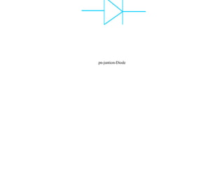
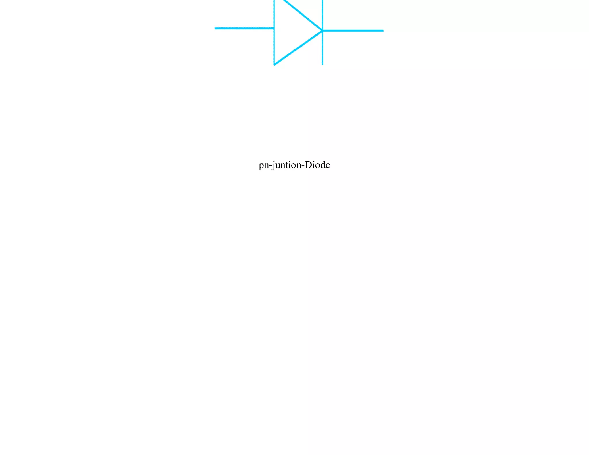
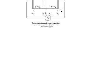
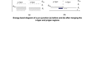
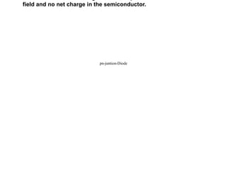
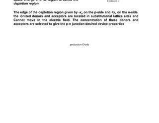
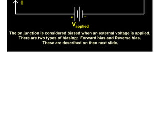
1) A pn junction diode consists of a p-type semiconductor joined to an n-type semiconductor. When the two materials come together, electrons from the n-type region combine with holes from the p-type region, leaving an uncharged depletion region.
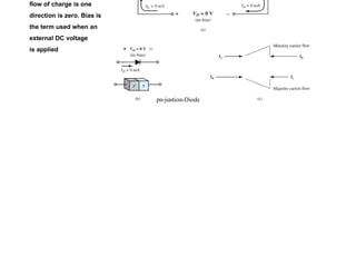
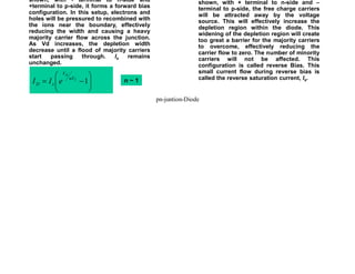
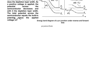
2) When a forward bias is applied, the depletion region narrows, lowering the barrier for majority carriers to flow across the junction. Under reverse bias, the depletion region widens, blocking most carrier flow.
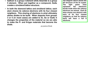
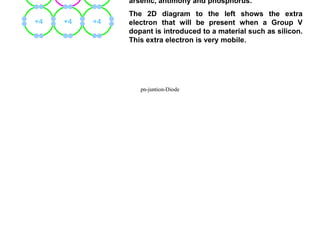
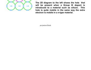
3) Diodes are commonly made from silicon or germanium as the base semiconductor material. Doping one region with elements from group III makes it p-type, while doping the other with elements from group V makes it n-type


![Polymer [ बहुलक ] Chemistry Notes PDF - Irfanullah Mehar - JJ Sir Chemistry.pdf](https://cdn.slidesharecdn.com/ss_thumbnails/polymerchemistrynotespdf-irfanullahmehar-jjsirchemistry-260210172118-3f9b37f7-thumbnail.jpg?width=640&height=640&fit=bounds)


