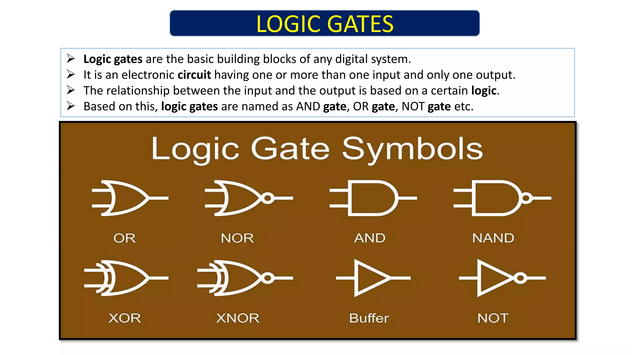
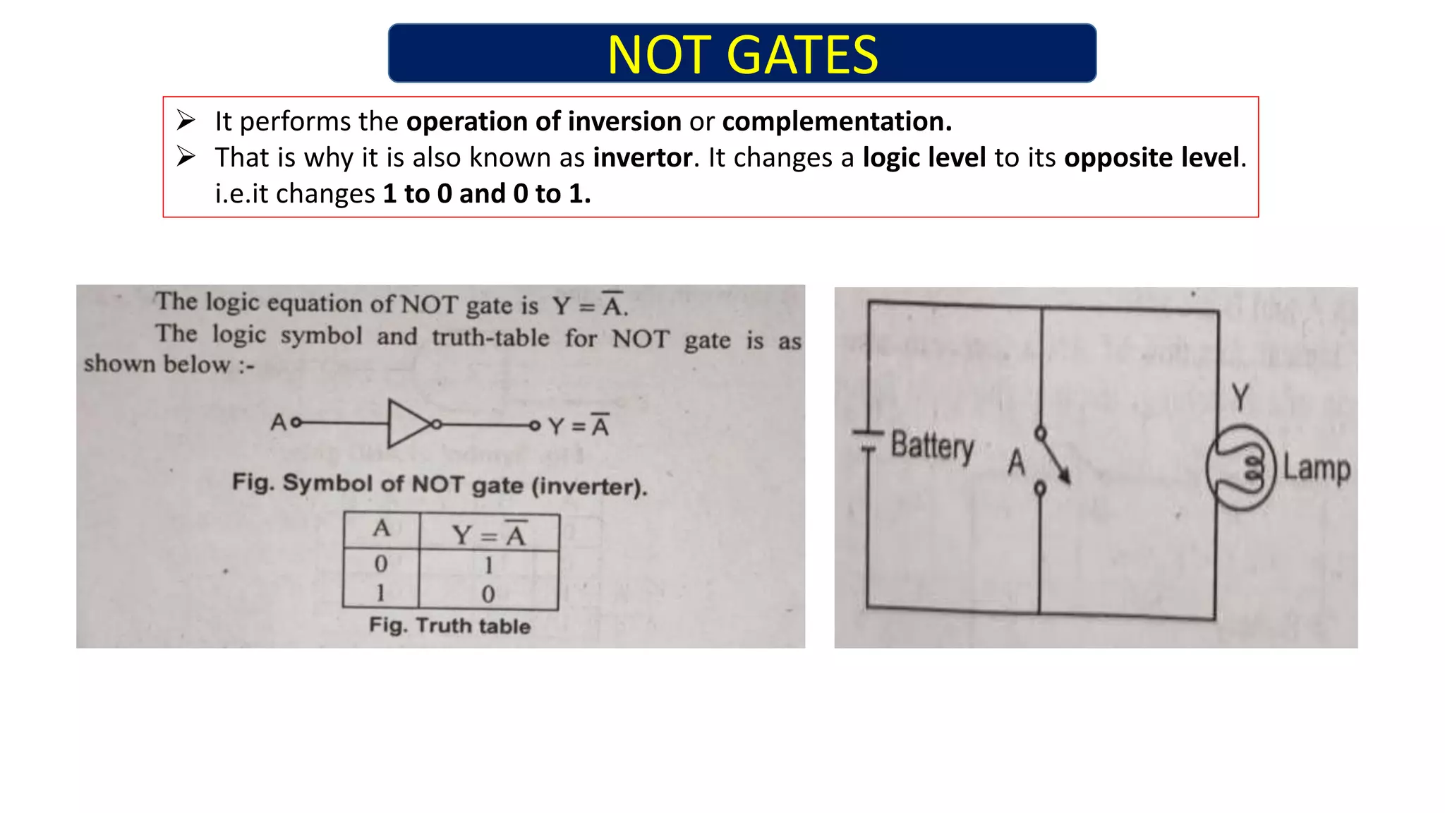
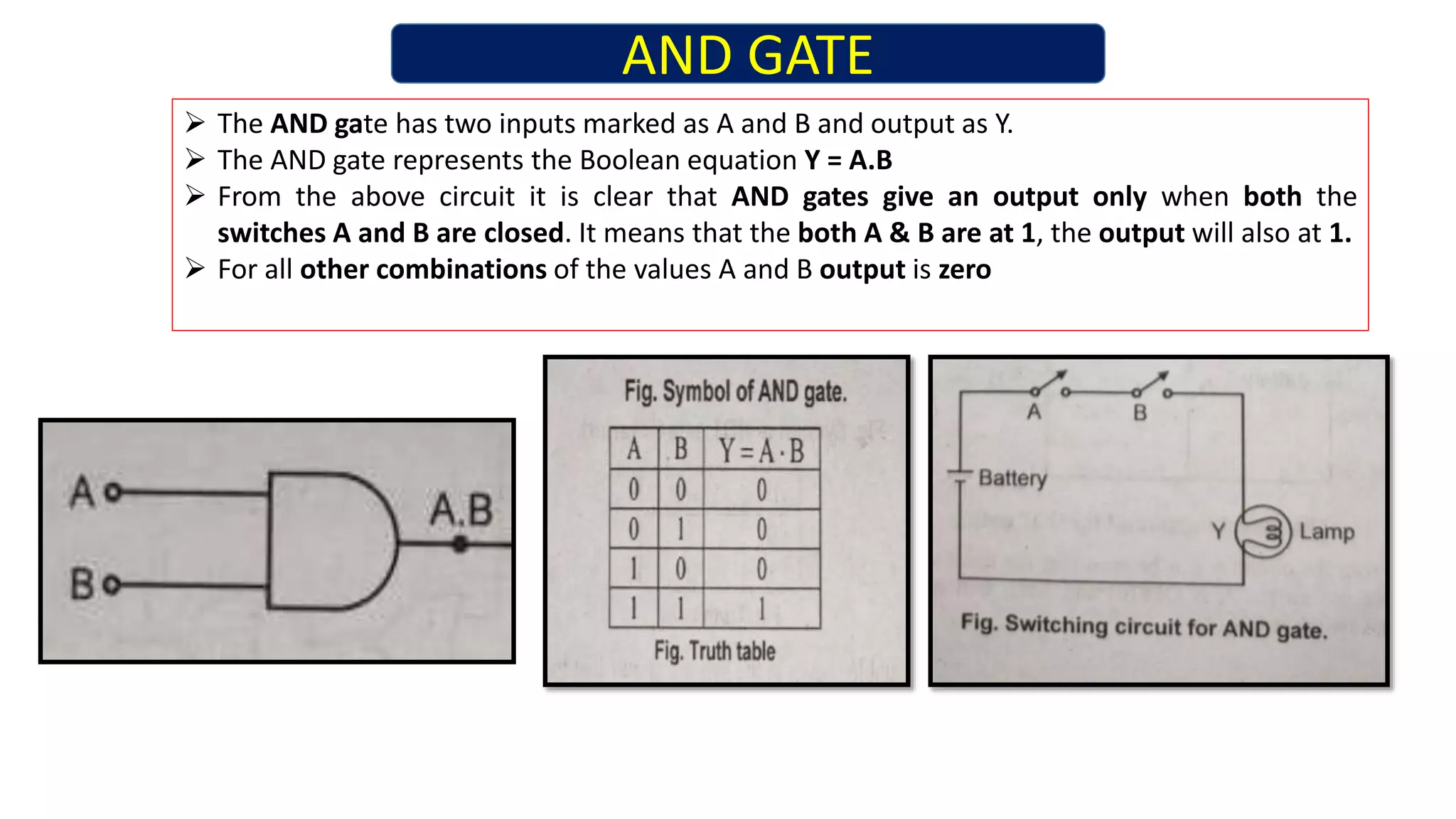
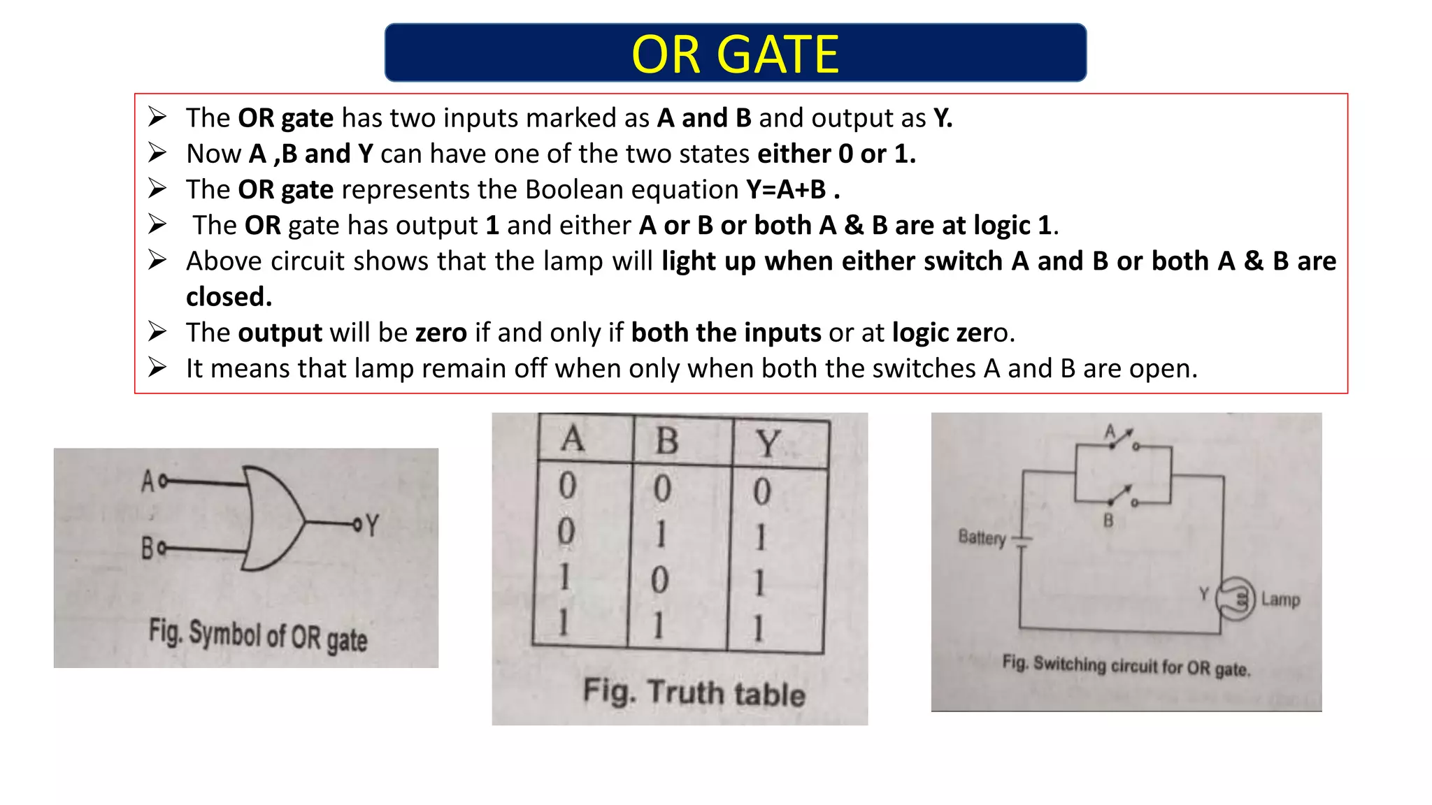
This document provides information about reversible logic gates and their application in field programmable gate arrays (FPGAs). It describes the design of reversible 4-to-1 multiplexers, D latches, and master-slave flip flops using novel reversible gates. The proposed reversible designs have fewer components and lower cost compared to existing irreversible circuit designs. In conclusion, the document presents the first proposed design of a reversible logic block for FPGAs, improving the efficiency of sequential circuits used to realize FPGA functions.
The document provides an overview of the Motorola DSP563xx family of processors. It describes the core architecture which includes a data ALU, MAC unit, address generation unit, program control unit, and on-chip memory. It also discusses the internal buses and on-chip peripherals. The DSP563xx family is used in applications such as wireless infrastructure and modem banks. Members of the family have different memory and peripheral configurations while sharing a standardized DSP56300 core.
This document provides an introduction to VHDL and behavioral modeling. It discusses how VHDL was developed to address the need for modeling increasingly complex digital circuits. VHDL allows designs to be specified at different levels of abstraction through behavioral, dataflow, and structural descriptions. The document reviews key VHDL concepts like libraries, entities, architectures, and sequential/concurrent statements. Examples are given to demonstrate how basic digital components can be modeled in VHDL including gates, multiplexers, and flip-flops.
This document discusses FPGA based system design. It begins with an introduction to digital system design approaches, including using discrete logic gates on a board versus using a single programmable chip. It then covers the evolution of programmable logic devices from simple PLDs like PLA and PAL, to more complex CPLDs, and finally modern FPGAs. FPGAs contain logic blocks, programmable routing switches, and I/O pads. Commercial FPGA products from companies like Xilinx and Altera are also mentioned.
The 8086 microprocessor has an architecture that separates it into a Bus Interface Unit (BIU) and Execution Unit (EU). The BIU fetches instructions and data from memory and handles address calculation on the buses. The EU decodes and executes instructions using its 16-bit ALU. The 8086 has 16 general purpose registers including 4 data registers (AX, BX, CX, DX) and segment/pointer registers. It also contains a flag register for storing status flags. The 8086 can queue up to 6 bytes of upcoming instructions to improve performance.
This document discusses digital integrated circuit design and the physical design process. It describes the key stages of digital design as electronic system level, RTL design, and physical design. Physical design involves steps like floorplanning, clustering/partitioning, placement, clock tree synthesis, and routing to lay out the design according to a technology library. Physical design categories include full custom, semi-custom, and pre-cast designs, which differ in the flexibility allowed in cell usage and placement/routing.
This document discusses the architecture of CPLDs and FPGAs. CPLDs consist of PAL-like blocks, I/O blocks, and a programmable interconnect structure. FPGAs consist of an array of configurable logic blocks, I/O blocks, and programmable row and column interconnect channels. The document compares CPLDs and FPGAs, noting that FPGAs have a more complex architecture and unpredictable delays while CPLDs are less complex, cheaper, and have more predictable delays. The conclusion restates that the document discussed the architecture of CPLDs and FPGAs and listed their comparisons.
FPGA are a special form of Programmable logic devices(PLDs) with higher densities as compared to custom ICs and capable of implementing functionality in a short period of time using computer aided design (CAD) software....by mathewsubin3388@gmail.com
The document discusses ARM7 multiplication instructions. It describes six instructions: MUL, MLA, UMULL, UMLAL, SMULL, and SMLAL. MUL multiplies two 32-bit registers and stores the lower 32 bits of the result. The other instructions multiply 32-bit registers to produce 64-bit results. UMULL, UMLAL, SMULL, and SMLAL retain all 64 bits of the product, while MLA also allows accumulating a multiplication with the contents of another register. Examples are given of using each instruction type.
This document provides an introduction to PIC microcontrollers. It discusses the architecture of PIC microcontrollers, including the 16C6x and 16C7x architectures. It describes the registers, memory, and instruction set of PIC microcontrollers. Some key points covered include the Harvard architecture, pipelining, addressing modes, arithmetic, logical, and conditional instructions. Peripherals like timers and interrupts are also mentioned.
The document provides an introduction to PIC microcontrollers, including:
- The PIC16C6X/7X family uses a Harvard architecture with separate program and data memory buses, allowing fast instruction execution.
- The CPU contains registers like the Working Register, Status Register, FSR, and 8-level stack.
- Memory is organized into program memory, data memory (register files) and stack.
- Upon reset, the PIC initializes registers and jumps to address 0 to begin program execution. Resets ensure the PIC starts in a known state.
Complex Programmable Logic Device (CPLD) Architecture and Its Applicationselprocus
A CPLD (complex programmable logic device) chip includes several circuit blocks on a single chip with inside wiring resources to attach the circuit blocks. Each circuit block is comparable to a PLA or a PAL.
This document provides an introduction to VLSI technology and MOS transistors. It discusses the history and generations of integrated circuits from SSI to VLSI. The dominant fabrication process for high performance VLSI circuits is now silicon CMOS technology. The document then describes the basic MOS transistor structure and different types of MOS transistors including nMOS, pMOS, and CMOS. It explains the working of enhancement mode and depletion mode transistors. Finally, it discusses CMOS fabrication processes like p-well and n-well and the basic structure of a p-well CMOS process.
This document provides an overview of system on chip (SoC) design. It discusses that a SoC integrates all components of an electronic system onto a single chip, and that SoC design involves identifying user needs and integrating various intellectual property blocks. The document then covers SoC fundamentals like the use of soft and hard IP cores, the design flow from specification to fabrication, and strategies for addressing SoC complexity through partitioning, abstraction levels, and reuse of pre-designed components.
ADC - Analog to Digital Conversion on AVR microcontroller Atmega16Robo India
Robo India in this PPT is explaining on the most crucial and important aspect of Embedded system, robotics, automation and physical computing.
Analog to digital conversion is required in almost every project of above mentioned domain. One advantage to use a AVR micro controller is that it has inbuilt ADC thus we donot need to use external system for ADC.
Here Robo India is teaching how to use ADC in AVR series microcontrollers.
We welcome your views and queries, we are found at-
website: http://roboindia.com
mail- info@roboindia.com
10.Design Of Two Pass Assembler in system software.pdfSwapnaliPawar27
A two-pass assembler operates in two phases. In pass 1, it scans the assembly code and builds symbol, literal, and pool tables to track labels, constants, and their locations. Pass 2 uses this information to convert assembly instructions into machine code by replacing labels with addresses and translating instructions into binary formats. The symbol table stores label names and addresses, while literal and pool tables manage constant values and where they are referenced to properly generate addresses in the final machine code output.
Interfacing methods of microcontrollerDiwaker Pant
The document discusses microcontroller interfacing. It defines interfacing as the transfer of data between microcontrollers and peripherals using buses. Interfacing is needed to connect a microcontroller's computation capabilities to external signals or devices to enable man-machine interaction. Various interfacing methods are described, including wiring techniques like wires, buses, and pins. Examples of interfacing a microcontroller to memory and I/O devices are provided. Common microcontroller interfaces like digital input/output, analog, serial interfaces are also summarized along with their applications and advantages/disadvantages.
The Advanced Microcontroller Bus Architecture (AMBA) specification defines interfaces for connecting processor and peripherals. It aims to standardize connections to enable modular system design. The Advanced Peripheral Bus (APB) is defined by AMBA for simple peripherals like timers and I/O. It uses few signals for non-pipelined transfers in two cycles to reduce power and complexity.
FPGAs can be programmed after manufacturing to implement custom logic functions. They contain programmable logic blocks and interconnects that can be configured to create custom circuits. FPGAs provide flexibility compared to ASICs but have higher per-unit costs. The FPGA architecture consists of configurable logic blocks, programmable interconnects, and I/O blocks. Configurable logic blocks contain LUTs that implement logic functions. Programmable interconnects connect the logic blocks, and I/O blocks interface with external components. FPGAs are commonly used for prototyping, emulation, parallel computing, and other applications that require customizable hardware.
The document discusses the structure and components of field programmable gate arrays (FPGAs). FPGAs consist of programmable logic blocks, interconnects, and input/output blocks. The logic blocks contain lookup tables and flip flops that can be programmed to implement desired logic functions. The interconnects include vertical and horizontal routing channels and switch boxes that allow the logic blocks to be connected as needed. The input/output blocks provide interfaces between the FPGA and external devices.
Application of code composer studio in digital signal processingIAEME Publication
This document discusses the Code Composer Studio (CCS) integrated development environment for digital signal processing applications on Texas Instruments processors. CCS provides tools for editing, building, debugging, and testing programs. It allows writing code in C/C++ and includes compilers, assemblers, linkers and debuggers. The document outlines the software development flow in CCS, including compiling, assembling, linking and debugging programs. It also provides steps for creating a new project in CCS and adding source files.
This presentation discusses the Lambda based design rules for drawing the layouts. The spacing between ltwo layers, extent if of overlap, minimum dimensions of each layer etc are decided by the lambda based design rules. the separation between metal and poly, poly and diffusion , width of metal etc
Programmable logic devices (PLDs) like PLA, PAL, CPLD and FPGA allow implementing logic circuits using programmable switches. PLA and PAL have programmable AND planes and OR planes to implement sum-of-products logic. PALs are simpler than PLAs with fixed OR planes. CPLDs contain multiple PAL-like blocks with programmable interconnects. FPGAs provide programmable logic blocks and interconnects to implement larger circuits without AND/OR planes. All PLDs require programming using CAD tools to set the switches for the desired logic function.
This document describes the design of a 0-9 binary coded decimal (BCD) counter circuit. It uses a 74LS90 BCD counter integrated circuit to generate the BCD codes from 0 to 9, and a 74LS47 7-segment display driver to decode and display the codes on a 7-segment display. The circuit was designed, breadboarded, and simulated in Digital Works to verify its functioning, counting from 0-9 each time a push button switch is pressed before resetting. Cascading multiple BCD counters can extend the counting range to larger numbers.
This document discusses the history and characteristics of CISC and RISC architectures. It describes how CISC architectures were developed in the 1950s-1970s to address hardware limitations at the time by allowing instructions to perform multiple operations. RISC architectures emerged in the late 1970s-1980s as hardware improved, focusing on simpler instructions that could be executed faster through pipelining. Common RISC and CISC processors used commercially are also outlined.
The document discusses various input/output interfacing components used with microprocessors, including parallel and serial communication interfaces, analog to digital and digital to analog converters, timers, and interrupt controllers. It describes the 8255 parallel interface chip, 8251 serial interface chip, and programming of ports and modes. Memory interfacing is also covered briefly. Application examples discussed include traffic light control, LED displays, and keyboard/display interfaces.
The document discusses basic and derived logic gates. It begins by introducing Boolean algebra and defining logic 0 and 1. It then explains the three basic logic gates - OR, AND, and NOT - through truth tables and circuit diagrams. The OR gate's output is 1 if any input is 1. The AND gate's output is 1 only if all inputs are 1. The NOT gate inverts the input. Complex logic circuits can be described algebraically using these basic gates and Boolean operations.
Digital logic gates and Boolean algebraSARITHA REDDY
The document discusses digital logic gates and Boolean algebra. It defines logic gates as electronic circuits that make logic decisions. Common logic gates include OR, AND, and NOT gates. Boolean algebra uses truth values of 0 and 1 instead of numbers, and has fundamental laws and operations for AND, OR, and NOT. Boolean algebra can be used to simplify logical expressions and save gates in digital circuit design.
boolean algrebra and logic gates in shortRojin Khadka
The document discusses logic gates and Boolean algebra. It describes the basic logic gates - OR, AND, NOT, NAND, NOR and XOR gates. It explains their symbols, truth tables and functions. Logic gates are electronic circuits that make logic decisions. Boolean algebra uses values of 0 and 1 instead of numbers. It has laws like commutative, associative and distributive laws that define operations on logic values. Logic gates and Boolean algebra are important for designing digital circuits and simplifying logical functions.
Physics investigatgory project on logic gates class 12appietech
This document describes various logic gates and their workings. It begins with introducing logic gates and their basic components like inputs, outputs, truth tables, and Boolean algebra. It then explains the OR gate, AND gate, NOT gate, NOR gate, NAND gate, EX-OR gate, and EX-NOR gate through their circuit diagrams and truth tables. Each gate is constructed using basic electronic components like diodes, transistors, and resistors. The document concludes that logic gates are fundamental building blocks of modern electronics and digital circuits.
The document describes various logic gates - OR, AND, NOT, NOR, and NAND. It provides the circuit design and truth tables for each gate. The OR gate can be realized using two diodes and will output 1 if either input is 1. The AND gate uses two diodes and a resistor, and will only output 1 if both inputs are 1. A NOT gate inverts the input and can be made with a transistor. A NOR gate consists of an OR gate followed by a NOT gate, while a NAND gate is an AND gate followed by a NOT.
physics investigatory project class 12 on logic gates ,boolean algebrasukhtej
The document discusses logic gates and their applications. It begins by defining logic gates and their basic components. It then provides details on designing and simulating various logic gate circuits including OR, AND, NOT, NOR, NAND, XOR, XNOR gates. Finally, it discusses some common applications of logic gates such as using OR gates to detect events, AND gates as enable/inhibit gates, XOR/XNOR gates for parity generation/checking, and NOT gates as inverters in oscillators.
The document discusses various logic gates like OR, AND, and NOT gates. It defines what each gate is, provides their truth tables and Boolean expressions, and includes examples of simple circuits to realize each gate using common electronic components like switches and bulbs. The document also acknowledges the sources used and provides an introduction, theory, and working of the OR, AND, and NOT gates along with the aim, components, theory, and working of sample circuits to demonstrate each gate.
The document discusses different digital logic components including logic gates, flip flops, registers, and counters. It describes the basic types of logic gates such as AND, OR, NOT, NAND, and NOR gates. It also discusses different types of flip flops including T, S-R, J-K, and D flip flops which are used to store binary data. Registers are formed using groups of flip flops to store multi-bit data. Counters are also discussed as another component of digital logic systems.
This document describes Virat Prasad's class project to design and simulate logic gate circuits. It includes an introduction to logic gates, descriptions of common logic gates like OR, AND, NOT, NOR and NAND gates. Truth tables and circuit diagrams are provided to explain the working of each gate. The document also acknowledges those who helped with the project and provided a bibliography.
This document discusses digital logic gates. It begins by defining a gate as a digital circuit with one or more inputs and one output. The three basic gates are described as the NOT, OR, and AND gates. Additional universal gates, the NAND and NOR gates, are introduced. Truth tables are provided to explain the output of each gate for all possible input combinations. The document also discusses how to derive different gate functions using NAND and NOR gates alone through De Morgan's theorems.
The document discusses different types of logic gates such as AND, OR, NAND, NOR gates. It defines each gate, explains their operation through truth tables and diagrams. The document serves as a report on logic gates submitted as part of a school physics project.
This document provides an overview of Boolean algebra and its applications in digital logic circuits. It defines Boolean algebra and its basic operations like AND, OR, and NOT. Boolean algebra represents true as 1 and false as 0 and is used to perform logical operations in digital computers and electronic circuits. The document describes the three basic logic gates - AND, OR, and NOT - and provides their truth tables. It also outlines some fundamental theorems of Boolean algebra like duality, properties of 0 and 1, commutative, associative, distributive, and De Morgan's laws. Finally, it provides some examples of applying these concepts to verify theorems and represent logic expressions as circuits.
This time I am presenting you Physics Investigatory Project for class 12 on the topic "TO DESIGN APPROPRIATE LOGIC GATE COMBINATION FOR GIVEN TRUTH TABLE"
The document is a physics project report submitted by Saurav Kumar of Class 12th Section A1. The report describes the design and simulation of various logic gates like OR, AND, NOT, NOR, NAND, XOR and XNOR gates. Circuit diagrams and truth tables are provided to explain the working principle of each logic gate. The project aims to design an appropriate logic gate for a given truth table.
This document describes a physics investigatory project on logic gates created by Simran Singh for their teacher Shazia Ma'am. It includes an introduction to logic gates, descriptions of common logic gates like OR, AND, NOT, NOR and NAND gates. It also provides the circuit diagrams and truth tables for each gate. Experiments were conducted to design and simulate each gate using a breadboard, switches, wires and a battery or bulb. In conclusion, the project provides hands-on experience with basic logic gates and their functioning.
Logic gates are basic electronic circuits that perform logical operations and produce binary outputs. The common logic gates are OR, AND, NOT, NAND, NOR, XOR, and XNOR. An OR gate output is 1 if one or more inputs are 1. An AND gate output is 1 only if all inputs are 1. A NOT gate inverts the input so its output is the opposite state. Combinations of gates can create more complex gates like NAND and NOR. Logic gates have applications in electronic devices like alarms and locks.
M. FLORENCE DAYANA/unit - II logic gates and circuits.pdfDr.Florence Dayana
Logic Gates, Truth Table, AND Gate
Types of Digital Logic AND Gate, The 2-input and 3-input AND Gate, OR Gate, Types of Digital Logic AND Gate, The 2-input OR gate, The 3-input OR gate, NOT Gate, NAND Gate, The 2-input NAND Gate, The 3-input NAND Gate, NOR Gate, 2-input NOR gate
Just like other gates, XOR gate or Exclusive-OR gate
This document describes a physics investigatory project on logic gates submitted by S. Kiruthiga of Kendriya Vidyalaya, Dharmapuri. It includes an introduction to logic gates, their basic principles and types including OR, AND, NOT, NOR and NAND gates. Circuit diagrams and truth tables are provided for each gate. The project was guided by [name removed] and certifies this as Kiruthiga's bona fide work.
Similar to LOGIC GATES VIDEO LECTURE IN HINDI|OR GATE,AND GATE &NOT GATE|LOGIC DIAGRAM &TRUTH TABLE OF GATES (20)
THERMAL BREAKDOWN|BREAKDOWN IN SOLIDS|HIGH VOLTAGE ENGINEERINGPrasant Kumar
The document discusses thermal breakdown in insulating materials when subjected to electric fields. It explains that the material heats up due to conduction current and dielectric losses from polarization. As temperature increases, conductivity rises as well, reaching a point of instability where the heat generated exceeds what can be dissipated, causing breakdown. Various heating curves are shown representing different electric stress levels as a function of specimen temperature. A thermal instability condition curve illustrates how breakdown occurs at fields E1 and E2 when heat generated surpasses heat lost at temperatures TA and TB.
BREAKDOWN OF SOLID DIELECTRICS|BREAKDOWN IN SOLIDS|HIGH VOLTAGE ENGINEERINGo...Prasant Kumar
The document discusses breakdown mechanisms in solid dielectric materials. Solid materials have higher breakdown strength than gases and liquids. When breakdown occurs in solids, the material is permanently damaged and cannot recover its original breakdown strength. The principal breakdown mechanisms for solids are intrinsic or ionic breakdown, electromechanical breakdown, thermal breakdown, electrochemical breakdown, and treeing and tracking. The breakdown mechanism depends on factors like temperature, impurities, and the time of voltage application.
STRESSED OIL VOLUME THEORY OF LIQUID DIELECTRICS|BREAKDOWN IN LIQUIDS|HIGH VO...Prasant Kumar
FOR YOUTUBE LINK OF ALL TOPICS
https://youtu.be/3zkBPYMPADw
ELECTRONIC BREAKDOWN OF LIQUID DIELECTRICS|HIGH VOLTAGE ENGINEERING|BREAKDOWN IN LIQUID DIELECTRICS
CONDUCTION & BREAKDOWN IN LIQUID DIELECTRICS|HIGH VOLTAGE ENGINEERING|ELECTRI...Prasant Kumar
This document discusses conduction and breakdown in liquid dielectrics. It explains that the breakdown voltage depends on factors like the electric field, gap separation, cathode work function, liquid viscosity, temperature, and molecular structure. The presence of dissolved gases, especially electronegative gases like oxygen, can increase the breakdown strength of liquids. Commercial liquids contain impurities like gas bubbles and suspended particles that reduce their breakdown strength. Finally, many external factors influence liquid dielectric breakdown, such as electrode configuration, material, size and finish, voltage type/period/magnitude, temperature, pressure, liquid purification, and aging condition.
PN JUNCTION DIODE IN हिंदी|FORWARD AND REVERSE BIASED OF DIODE|BASIC ELECTRON...Prasant Kumar
This document discusses the basics of a PN junction diode. It explains that a PN junction diode consists of a positive P-type region and negative N-type region fused together. It describes forward bias as applying voltage such that the positive terminal is connected to the P-side and negative to the N-side, causing current to flow. Reverse bias is applying the opposite voltage configuration, widening the depletion region and preventing current from flowing. The document provides an overview of PN junction diode characteristics and biasing methods.
Communicating effectively and consistently with students can help them feel at ease during their learning experience and provide the instructor with a communication trail to track the course's progress. This workshop will take you through constructing an engaging course container to facilitate effective communication.
Strategies for Effective Upskilling is a presentation by Chinwendu Peace in a Your Skill Boost Masterclass organisation by the Excellence Foundation for South Sudan on 08th and 09th June 2024 from 1 PM to 3 PM on each day.
it describes the bony anatomy including the femoral head , acetabulum, labrum . also discusses the capsule , ligaments . muscle that act on the hip joint and the range of motion are outlined. factors affecting hip joint stability and weight transmission through the joint are summarized.
Main Java[All of the Base Concepts}.docxadhitya5119
This is part 1 of my Java Learning Journey. This Contains Custom methods, classes, constructors, packages, multithreading , try- catch block, finally block and more.
हिंदी वर्णमाला पीपीटी, hindi alphabet PPT presentation, hindi varnamala PPT, Hindi Varnamala pdf, हिंदी स्वर, हिंदी व्यंजन, sikhiye hindi varnmala, dr. mulla adam ali, hindi language and literature, hindi alphabet with drawing, hindi alphabet pdf, hindi varnamala for childrens, hindi language, hindi varnamala practice for kids, https://www.drmullaadamali.com
Leveraging Generative AI to Drive Nonprofit InnovationTechSoup
In this webinar, participants learned how to utilize Generative AI to streamline operations and elevate member engagement. Amazon Web Service experts provided a customer specific use cases and dived into low/no-code tools that are quick and easy to deploy through Amazon Web Service (AWS.)
How to Make a Field Mandatory in Odoo 17Celine George
In Odoo, making a field required can be done through both Python code and XML views. When you set the required attribute to True in Python code, it makes the field required across all views where it's used. Conversely, when you set the required attribute in XML views, it makes the field required only in the context of that particular view.
2. LOGIC GATES
Logic gates are the basic building blocks of any digital system.
It is an electronic circuit having one or more than one input and only one output.
The relationship between the input and the output is based on a certain logic.
Based on this, logic gates are named as AND gate, OR gate, NOT gate etc.
3. It performs the operation of inversion or complementation.
That is why it is also known as invertor. It changes a logic level to its opposite level.
i.e.it changes 1 to 0 and 0 to 1.
NOT GATES
4. AND GATE
The AND gate has two inputs marked as A and B and output as Y.
The AND gate represents the Boolean equation Y = A.B
From the above circuit it is clear that AND gates give an output only when both the
switches A and B are closed. It means that the both A & B are at 1, the output will also at 1.
For all other combinations of the values A and B output is zero
5. OR GATE
The OR gate has two inputs marked as A and B and output as Y.
Now A ,B and Y can have one of the two states either 0 or 1.
The OR gate represents the Boolean equation Y=A+B .
The OR gate has output 1 and either A or B or both A & B are at logic 1.
Above circuit shows that the lamp will light up when either switch A and B or both A & B are
closed.
The output will be zero if and only if both the inputs or at logic zero.
It means that lamp remain off when only when both the switches A and B are open.