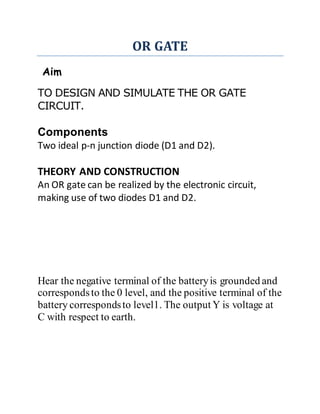
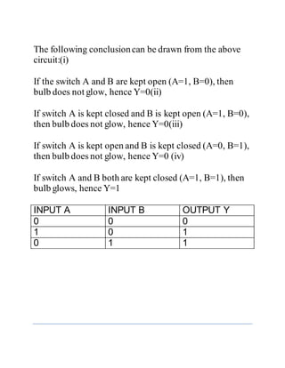
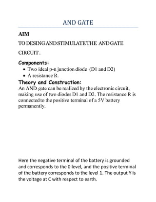
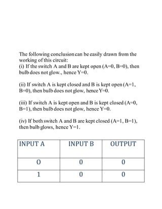
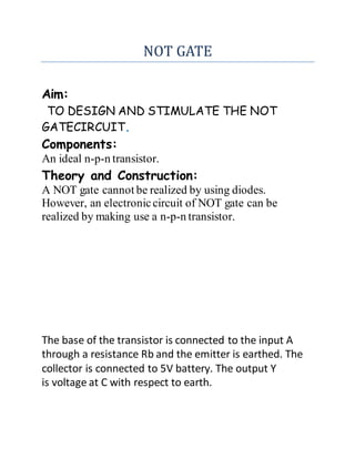
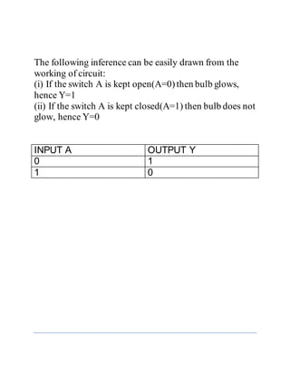
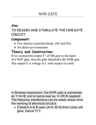
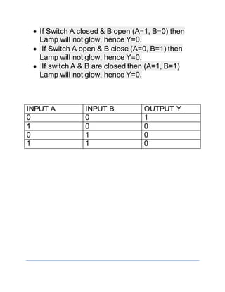
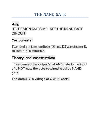
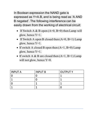
AIM
To design an appropriate logic gate
combination for a given truth table
INTRODUCTION
GATE-A gate is defined as a digital circuit
which follows some logical relationship between
the input and output voltages. It a digital circuit
which allows signal to pass through as stop.
LOGIC GATE- A logic gate is an elementary
building block of a digital circuit. It makes
“logical decisions” based on the different
combinations of digital signals present on its
inputs. Digital logic gates may have more than
one input but generally only have one digital
output. Most logic gates have two inputs and
one output.
A logic gate may have one or more input, but it
has only one output. The relation between the
possible values of input and output voltage is
expressed in the form of table called truth table
or table of combination.
GEORGE BOOLE in 1980 invented a different
kind if algebra based on binary nature at the
logic, this algebra of logic is called BOOLEAN
ALGEBRA. A logical statement can have only
two values, such as HIGH/LOW, ON/OFF,
CLOSED/OPEN, YES/NO, RIGHT/WRONG,
TRUE/FALSE, COUNDUCTING/NON-
COUNDICTING etc. The two values of logic
statement one denoted by the binary number 1
and 0. The binary number 1 is used to denote
high value. The logical statements that logical
gates follow are called Boolean Expression.
LOGIC GATES AND INTEGRATED
CIRCUITS
Logic gates are primarily implemented
electronically using diodes or transistors, but
can also be constructed using electromagnetic
relays logic", fluidic logic, pneumatic
logic, optics, molecules, or even mechanical
elements. With amplification, logic gates can be
cascaded in the same way that Boolean
functions can be composed, allowing the
construction of a physical model of all of
Boolean logic, and therefore, all of the
algorithms and mathematics that can be
described with Boolean logic.
A large number of electronic circuits in
computers, control units, and so on" are made
up of logic gates. These process signals
represent either true or false. $he most
common symbols used to represent logic gates
are shown below.
BASIC GATES
The OR Gate: -
It is a device that combines A and B to give Y as the
result. The OR gate has two or more inputs and one
output. In Boolean algebra, addition symbol (+), is
referred as the OR. The Boolean expression:
A+B=Y
This indicates that Y equals to A or B.
The AND Gate: -
It is a device that combines A with B to give Y as
the result. The AND gate has two or more inputs and
one output. In Boolean algebra, multiplication sign
is referred as the AND. The Boolean expression:
A.B=Y
or
A X B=Y
This indicates that Y equals to A and B.
The NOT Gate: -
It is a device that inverts the inputs. The NOT has
one input and has one output. In Boolean algebra,
bar symbol is referred as the NOT.
The Boolean expression:
A = Y
This indicates that Y is not equal to A.
OR GATE
Aim
TO DESIGN AND SIMULATE THE OR GATE
CIRCUIT.
Components
Two ideal p-n junction diode (D1 and D2).
THEORY AND CONSTRUCTION
An OR gate can be realized by the electronic circuit,
making use of two diodes D1 and D2.
Hear the negative terminal of the batteryis grounded and
correspondsto the 0 level, and the positive terminal of the
battery correspondsto level1. The output Y is voltage at
C with respect to earth.
The following conclusioncan be drawn from the above
circuit:(i)
If the switch A and B are kept open (A=1, B=0), then
bulb does not glow, hence Y=0(ii)
If switch A is kept closed and B is kept open (A=1, B=0),
then bulb does not glow, hence Y=0(iii)
If switch A is kept open and B is kept closed (A=0, B=1),
then bulb does not glow, hence Y=0 (iv)
If switch A and B both are kept closed (A=1, B=1), then
bulb glows, hence Y=1
INPUT A INPUT B OUTPUT Y
0 0 0
1 0 1
0 1 1
AND GATE
AIM
TODESINGANDSTIMULATETHE ANDGATE
CIRCUIT.
Components:
 Two ideal p-n junction diode (D1 and D2)
 A resistance R.
Theory and Construction:
An AND gate can be realized by the electronic circuit,
making use of two diodes D1 and D2. The resistance R is
connectedto the positive terminal of a 5V battery
permanently.
Here the negative terminal of the battery is grounded
and corresponds to the 0 level, and the positive terminal
of the battery corresponds to the level 1. The output Y is
the voltage at C with respect to earth.
The following conclusioncan be easily drawn from the
working of this circuit:
(i) If the switch A and B are kept open (A=0, B=0), then
bulb does not glow., hence Y=0.
(ii) If switch A is kept closed and B is kept open (A=1,
B=0), then bulb does not glow, henceY=0.
(iii) If switch A is kept open and B is kept closed (A=0,
B=1), then bulb does not glow, hence Y=0.
(iv) If both switch A and B are kept closed (A=1, B=1),
then bulb glows, hence Y=1.
INPUT A INPUT B OUTPUT
O 0 0
1 0 0
0 1 0
1 1 1
NOT GATE
Aim:
TO DESIGN AND STIMULATE THE NOT
GATECIRCUIT.
Components:
An ideal n-p-n transistor.
Theory and Construction:
A NOT gate cannot be realized by using diodes.
However, an electroniccircuit of NOT gate can be
realized by making use a n-p-n transistor.
The base of the transistor is connected to the input A
through a resistance Rb and the emitter is earthed. The
collector is connected to 5V battery. The output Y
is voltage at C with respect to earth.
The following inference can be easily drawn from the
working of circuit:
(i) If the switch A is kept open(A=0)then bulb glows,
hence Y=1
(ii) If the switch A is kept closed(A=1) then bulb does not
glow, hence Y=0
INPUT A OUTPUT Y
0 1
1 0
NOR GATE
Aim:
TO DESIGN AND STIMULATE THE NOR GATE
CIRCUIT.
Component:
 Two ideal p-n junction diode (D1 and D2).
 An ideal n-p-n transistor
Theory and Construction:
If we connect the outputY’ of OR gate to the input
of a NOT gate, then the gate obtained is the NOR gate.
The outputY is voltage at C with respect to earth
In Boolean expression, the NOR gate is expressed
as Y=A+B, and is being read as ‘A OR B negated’.
The following interference can be easily drawn from
the working of electrical circuit is
 If Switch A & B open (A=0, B=0) then Lamp will
glow, hence Y=1.
 If Switch A closed & B open (A=1, B=0) then
Lamp will not glow, hence Y=0.
 If Switch A open & B close (A=0, B=1) then
Lamp will not glow, hence Y=0.
 If switch A & B are closed then (A=1, B=1)
Lamp will not glow, hence Y=0.
INPUT A INPUT B OUTPUT Y
0 0 1
1 0 0
0 1 0
1 1 0
THE NAND GATE
Aim:
TO DESIGN AND SIMULATE THE NAND GATE
CIRCUIT.
Components:
Two ideal p-n junction diode (D1 and D2),a resistance R,
an ideal n-p- n transistor.
Theory and construction:
If we connect the output Y’ of AND gate to the input
of a NOT gate the gate obtained is called NAND
gate.
The output Y is voltage at C w.r.t. earth.
In Boolean expression the NAND gate is
expressed as Y=A.B, and is being read as ‘A AND
B negated’. The following interference can be
easily drawn from the working of electrical circuit:
 If Switch A & B open (A=0, B=0) then Lamp will
glow, hence Y=1.
 If Switch A open B closed then (A=0, B=1) Lamp
glow, hence Y=1.
 If switch A closed B open then (A=1, B=0) Lamp
glow, hence Y=1.
 If switch A & B are closed then (A=1, B=1) Lamp
will not glow, hence Y=0.
INPUT A INPUT B OUTPUT Y
0 0 1
1 0 1
0 1 1
1 1 0
BIBLIOGRAPHY
I obtained my information on this topic through-
 Slideshare.com
 Wikipedia.org
 Physics manual

physics investigatory on logic gates

  • 1.
    AIM To design anappropriate logic gate combination for a given truth table
  • 2.
    INTRODUCTION GATE-A gate isdefined as a digital circuit which follows some logical relationship between the input and output voltages. It a digital circuit which allows signal to pass through as stop. LOGIC GATE- A logic gate is an elementary building block of a digital circuit. It makes “logical decisions” based on the different combinations of digital signals present on its inputs. Digital logic gates may have more than one input but generally only have one digital output. Most logic gates have two inputs and one output. A logic gate may have one or more input, but it has only one output. The relation between the possible values of input and output voltage is expressed in the form of table called truth table or table of combination.
  • 3.
    GEORGE BOOLE in1980 invented a different kind if algebra based on binary nature at the logic, this algebra of logic is called BOOLEAN ALGEBRA. A logical statement can have only two values, such as HIGH/LOW, ON/OFF, CLOSED/OPEN, YES/NO, RIGHT/WRONG, TRUE/FALSE, COUNDUCTING/NON- COUNDICTING etc. The two values of logic statement one denoted by the binary number 1 and 0. The binary number 1 is used to denote high value. The logical statements that logical gates follow are called Boolean Expression.
  • 4.
    LOGIC GATES ANDINTEGRATED CIRCUITS Logic gates are primarily implemented electronically using diodes or transistors, but can also be constructed using electromagnetic relays logic", fluidic logic, pneumatic logic, optics, molecules, or even mechanical elements. With amplification, logic gates can be cascaded in the same way that Boolean functions can be composed, allowing the construction of a physical model of all of Boolean logic, and therefore, all of the algorithms and mathematics that can be described with Boolean logic. A large number of electronic circuits in computers, control units, and so on" are made up of logic gates. These process signals represent either true or false. $he most common symbols used to represent logic gates are shown below.
  • 5.
    BASIC GATES The ORGate: - It is a device that combines A and B to give Y as the result. The OR gate has two or more inputs and one output. In Boolean algebra, addition symbol (+), is referred as the OR. The Boolean expression: A+B=Y This indicates that Y equals to A or B. The AND Gate: - It is a device that combines A with B to give Y as the result. The AND gate has two or more inputs and one output. In Boolean algebra, multiplication sign is referred as the AND. The Boolean expression: A.B=Y or A X B=Y This indicates that Y equals to A and B.
  • 6.
    The NOT Gate:- It is a device that inverts the inputs. The NOT has one input and has one output. In Boolean algebra, bar symbol is referred as the NOT. The Boolean expression: A = Y This indicates that Y is not equal to A.
  • 7.
    OR GATE Aim TO DESIGNAND SIMULATE THE OR GATE CIRCUIT. Components Two ideal p-n junction diode (D1 and D2). THEORY AND CONSTRUCTION An OR gate can be realized by the electronic circuit, making use of two diodes D1 and D2. Hear the negative terminal of the batteryis grounded and correspondsto the 0 level, and the positive terminal of the battery correspondsto level1. The output Y is voltage at C with respect to earth.
  • 8.
    The following conclusioncanbe drawn from the above circuit:(i) If the switch A and B are kept open (A=1, B=0), then bulb does not glow, hence Y=0(ii) If switch A is kept closed and B is kept open (A=1, B=0), then bulb does not glow, hence Y=0(iii) If switch A is kept open and B is kept closed (A=0, B=1), then bulb does not glow, hence Y=0 (iv) If switch A and B both are kept closed (A=1, B=1), then bulb glows, hence Y=1 INPUT A INPUT B OUTPUT Y 0 0 0 1 0 1 0 1 1
  • 9.
    AND GATE AIM TODESINGANDSTIMULATETHE ANDGATE CIRCUIT. Components: Two ideal p-n junction diode (D1 and D2)  A resistance R. Theory and Construction: An AND gate can be realized by the electronic circuit, making use of two diodes D1 and D2. The resistance R is connectedto the positive terminal of a 5V battery permanently. Here the negative terminal of the battery is grounded and corresponds to the 0 level, and the positive terminal of the battery corresponds to the level 1. The output Y is the voltage at C with respect to earth.
  • 10.
    The following conclusioncanbe easily drawn from the working of this circuit: (i) If the switch A and B are kept open (A=0, B=0), then bulb does not glow., hence Y=0. (ii) If switch A is kept closed and B is kept open (A=1, B=0), then bulb does not glow, henceY=0. (iii) If switch A is kept open and B is kept closed (A=0, B=1), then bulb does not glow, hence Y=0. (iv) If both switch A and B are kept closed (A=1, B=1), then bulb glows, hence Y=1. INPUT A INPUT B OUTPUT O 0 0 1 0 0
  • 11.
  • 12.
    NOT GATE Aim: TO DESIGNAND STIMULATE THE NOT GATECIRCUIT. Components: An ideal n-p-n transistor. Theory and Construction: A NOT gate cannot be realized by using diodes. However, an electroniccircuit of NOT gate can be realized by making use a n-p-n transistor. The base of the transistor is connected to the input A through a resistance Rb and the emitter is earthed. The collector is connected to 5V battery. The output Y is voltage at C with respect to earth.
  • 13.
    The following inferencecan be easily drawn from the working of circuit: (i) If the switch A is kept open(A=0)then bulb glows, hence Y=1 (ii) If the switch A is kept closed(A=1) then bulb does not glow, hence Y=0 INPUT A OUTPUT Y 0 1 1 0
  • 14.
    NOR GATE Aim: TO DESIGNAND STIMULATE THE NOR GATE CIRCUIT. Component:  Two ideal p-n junction diode (D1 and D2).  An ideal n-p-n transistor Theory and Construction: If we connect the outputY’ of OR gate to the input of a NOT gate, then the gate obtained is the NOR gate. The outputY is voltage at C with respect to earth In Boolean expression, the NOR gate is expressed as Y=A+B, and is being read as ‘A OR B negated’. The following interference can be easily drawn from the working of electrical circuit is  If Switch A & B open (A=0, B=0) then Lamp will glow, hence Y=1.
  • 15.
     If SwitchA closed & B open (A=1, B=0) then Lamp will not glow, hence Y=0.  If Switch A open & B close (A=0, B=1) then Lamp will not glow, hence Y=0.  If switch A & B are closed then (A=1, B=1) Lamp will not glow, hence Y=0. INPUT A INPUT B OUTPUT Y 0 0 1 1 0 0 0 1 0 1 1 0
  • 16.
    THE NAND GATE Aim: TODESIGN AND SIMULATE THE NAND GATE CIRCUIT. Components: Two ideal p-n junction diode (D1 and D2),a resistance R, an ideal n-p- n transistor. Theory and construction: If we connect the output Y’ of AND gate to the input of a NOT gate the gate obtained is called NAND gate. The output Y is voltage at C w.r.t. earth.
  • 17.
    In Boolean expressionthe NAND gate is expressed as Y=A.B, and is being read as ‘A AND B negated’. The following interference can be easily drawn from the working of electrical circuit:  If Switch A & B open (A=0, B=0) then Lamp will glow, hence Y=1.  If Switch A open B closed then (A=0, B=1) Lamp glow, hence Y=1.  If switch A closed B open then (A=1, B=0) Lamp glow, hence Y=1.  If switch A & B are closed then (A=1, B=1) Lamp will not glow, hence Y=0. INPUT A INPUT B OUTPUT Y 0 0 1 1 0 1 0 1 1 1 1 0
  • 18.
    BIBLIOGRAPHY I obtained myinformation on this topic through-  Slideshare.com  Wikipedia.org  Physics manual