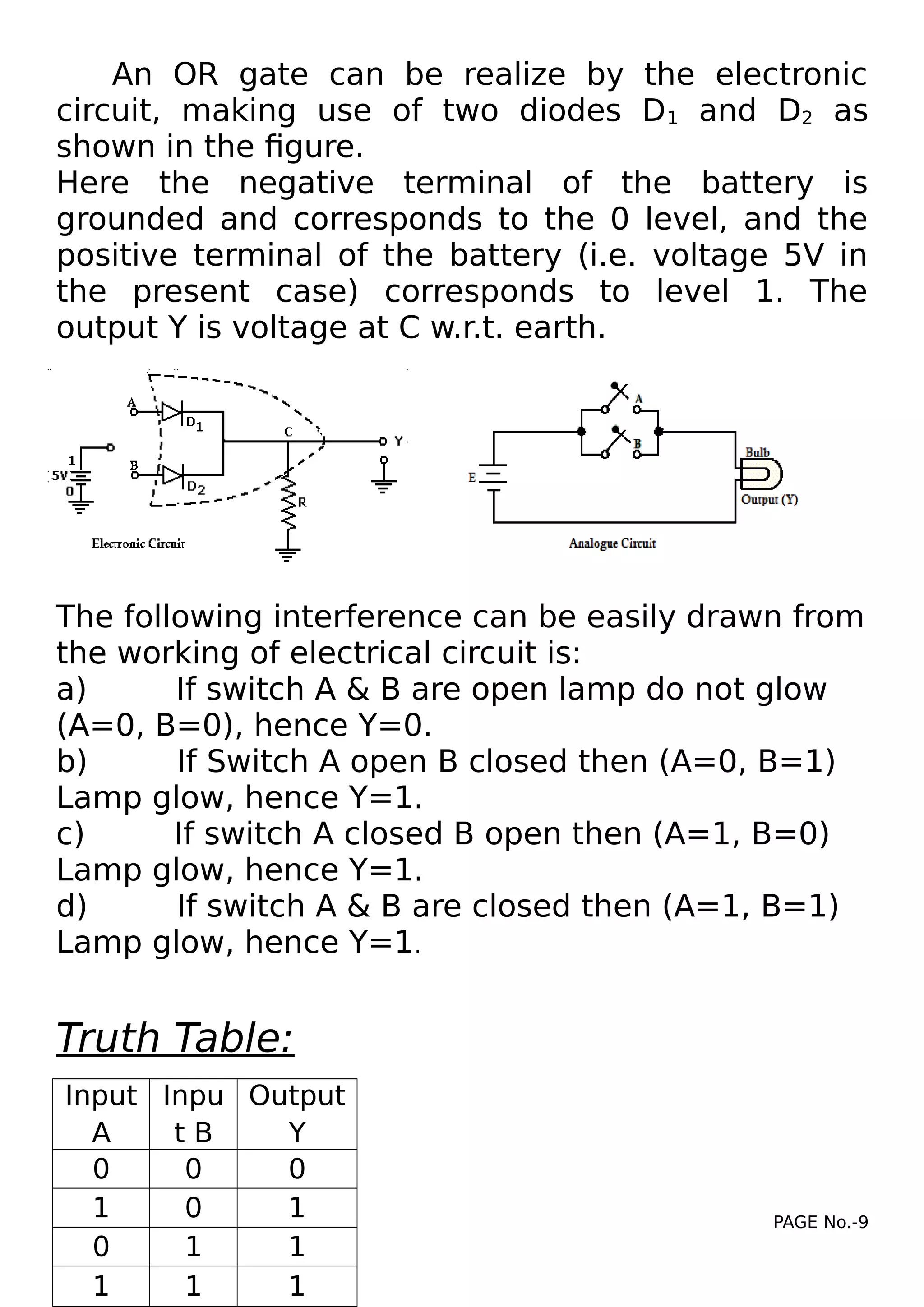
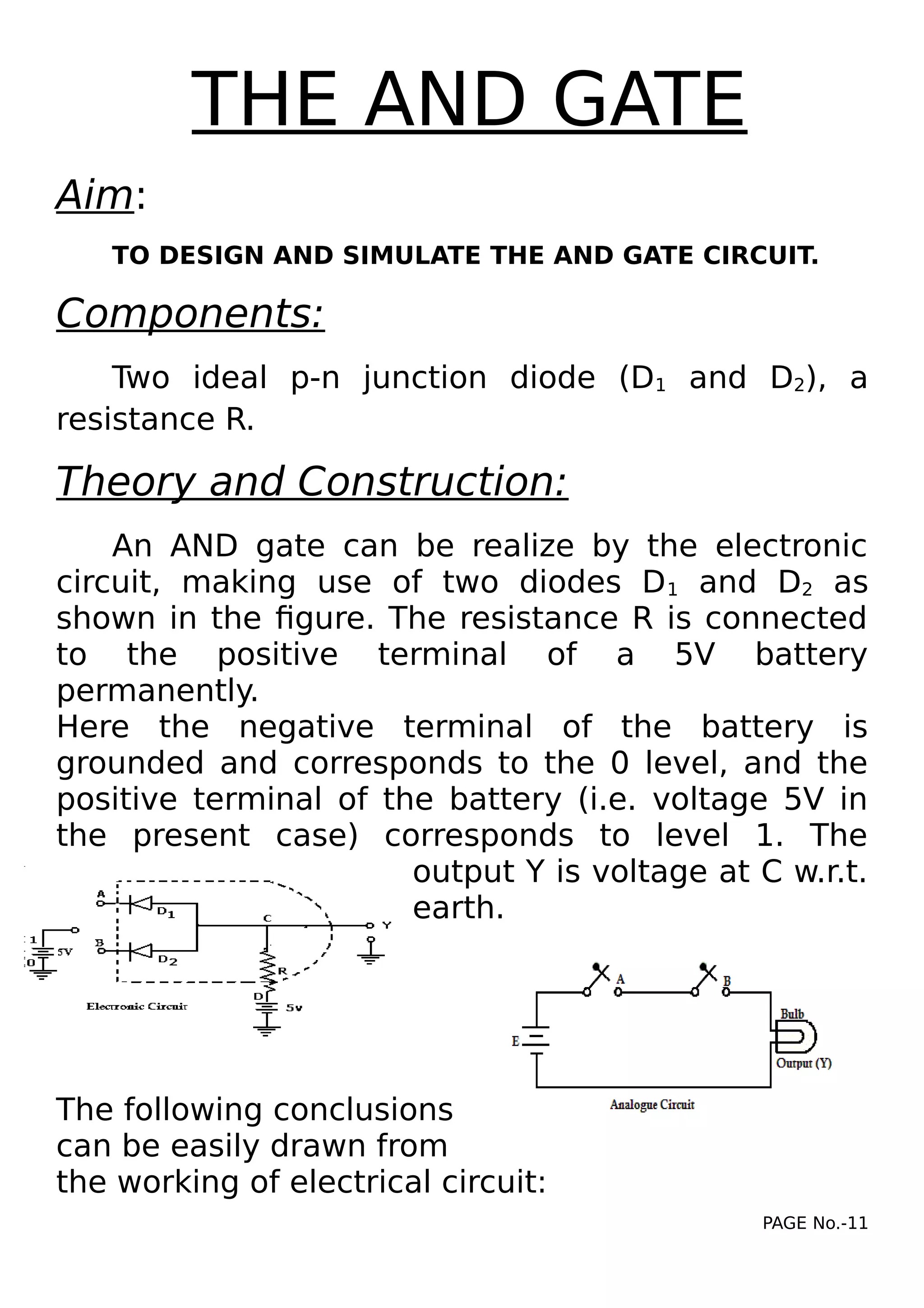
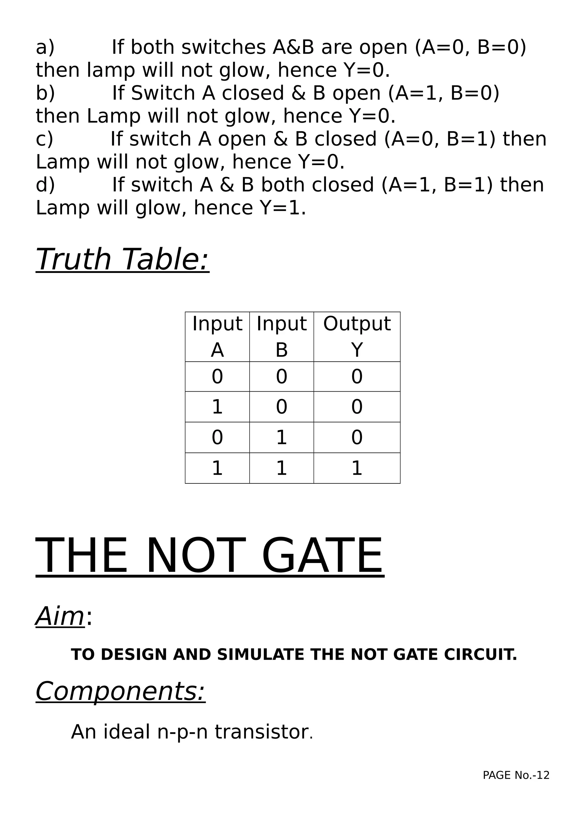
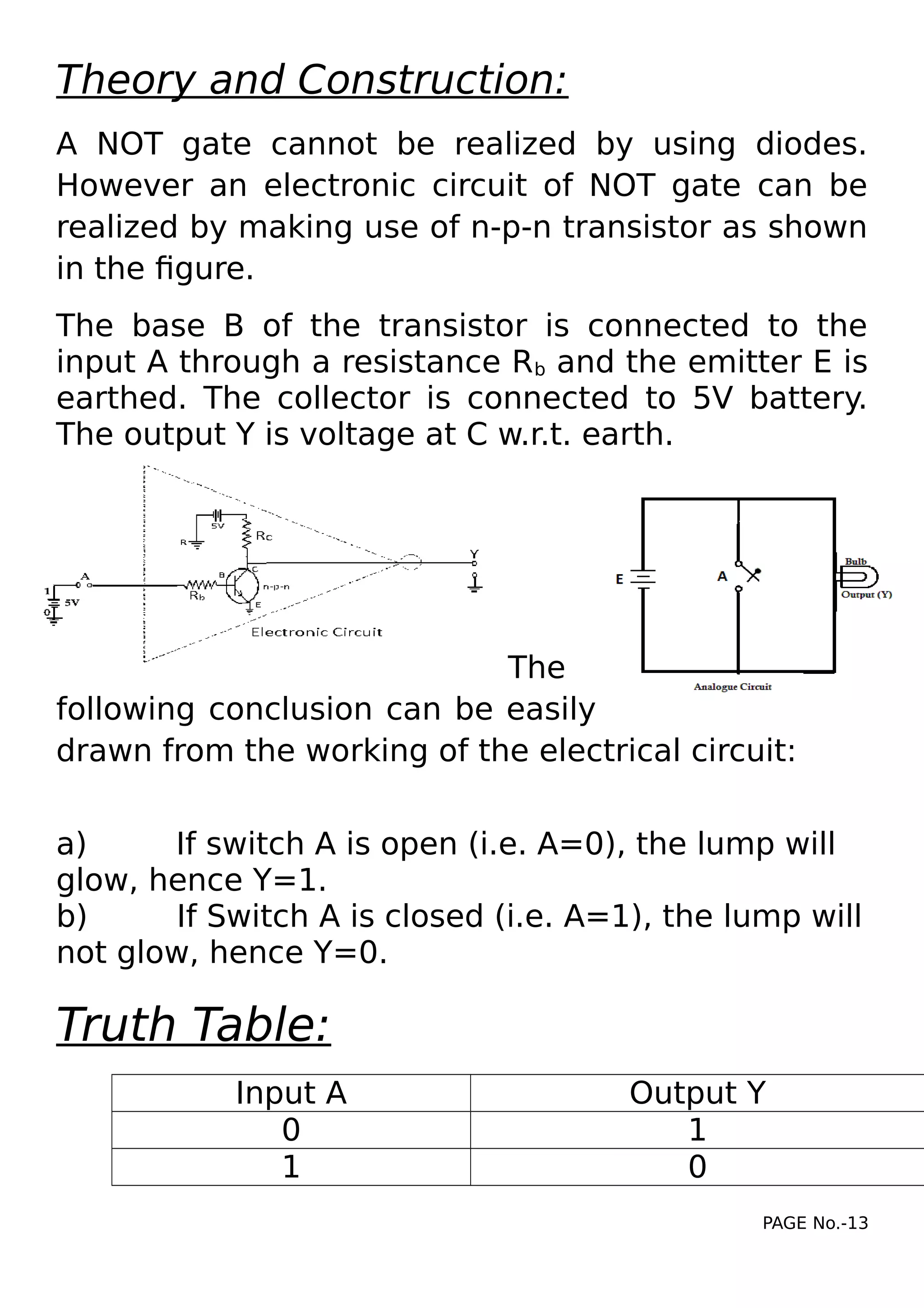
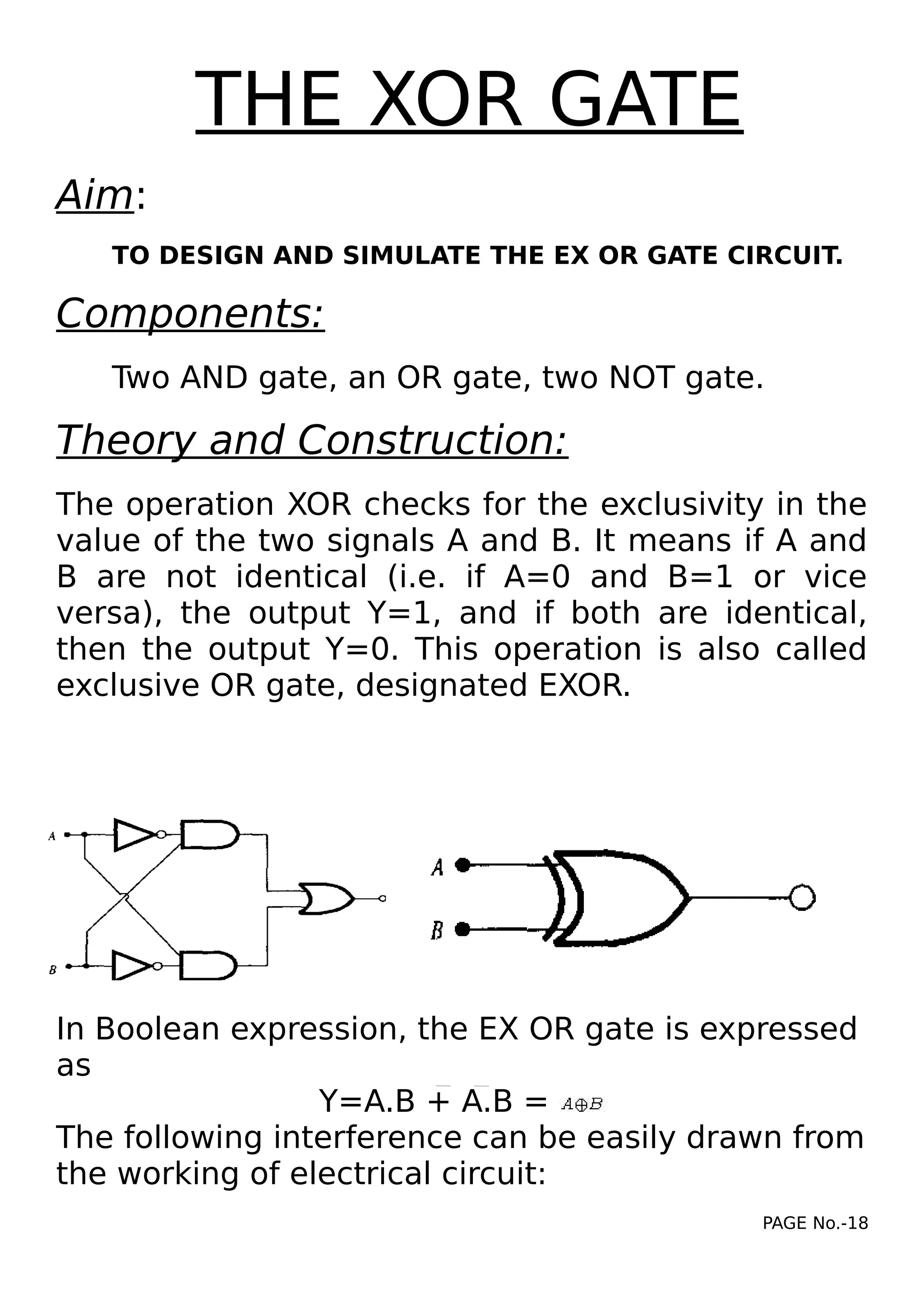
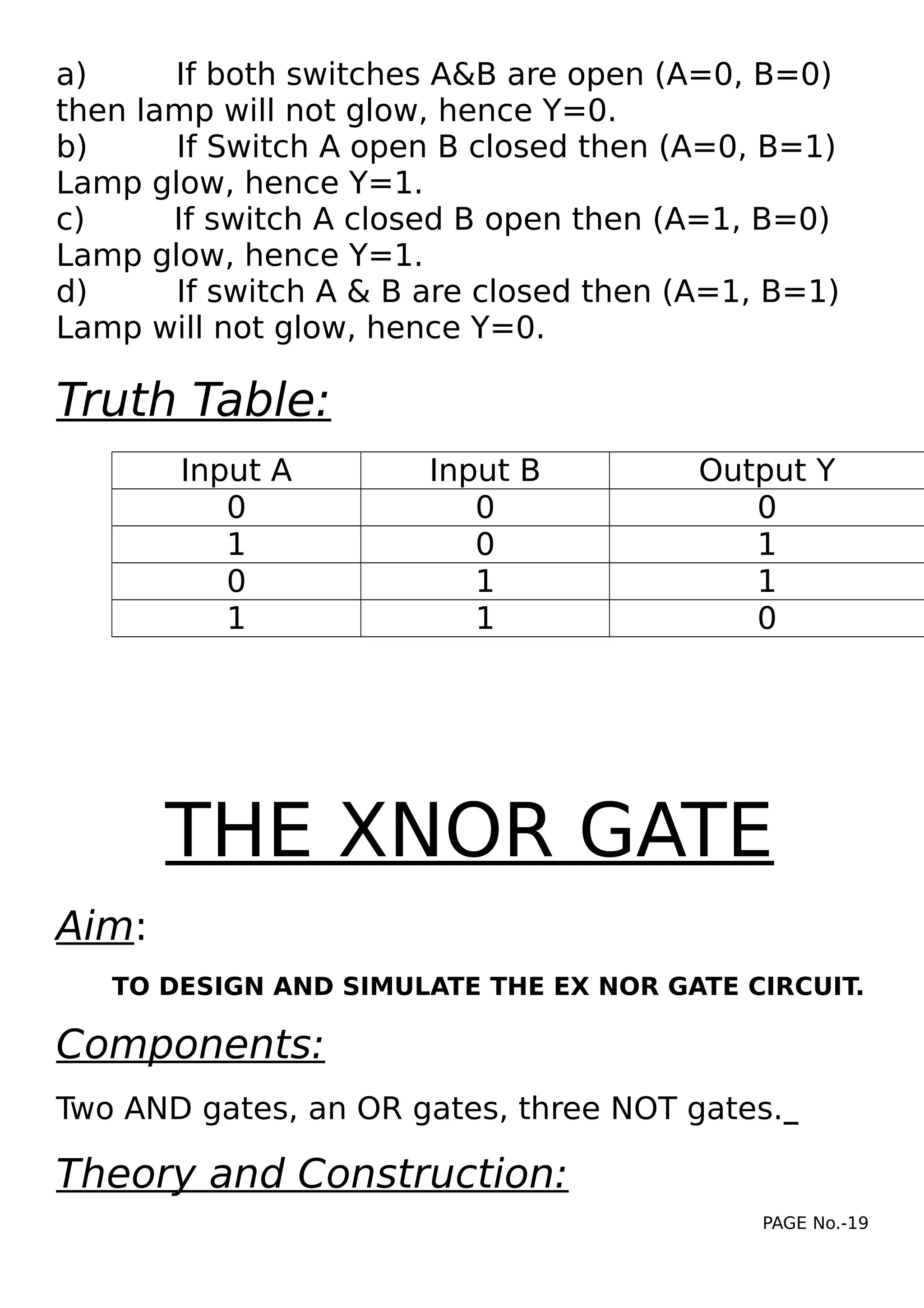
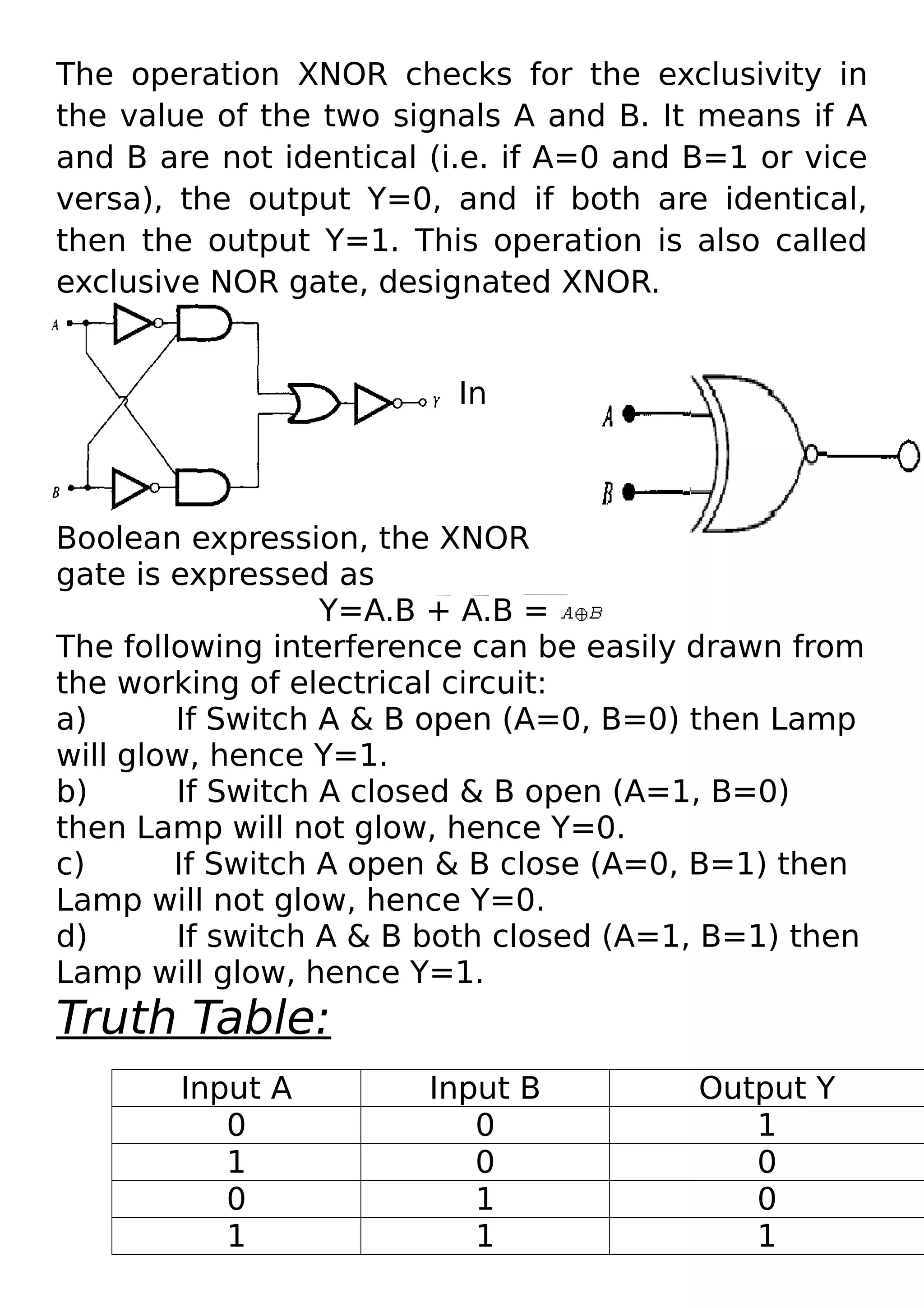
PHYSICS PROJECT
ON
LOGIC GATE
NAME: SAURAV KUMAR
CLASS: XIIth SECTION: 'A1'
ROLL NO.: 03
GUIDED BY: MISS ANUPAMA KAUSHAL
SCHOOL: B.D. PUBLIC SCHOOL
CERTIFICATE
PAGE No.-1
THIS IS TO CERTIFY THAT THIS PROJECT IS THE BONAFIDE WORK OF
SAURAV KUMAR OF CLASS 12TH 'A1' AND HAS BEEN
SUCCESSFULLY COMPLETED AND IS TAKEN TO BE AN ISSUE
CONDUCTED BY THE C.B.S.E. IN THE SESSION 2015-2016.
 TEACHER’S SIGNATURE:
 EXTERNAL’S SIGNATURE:
 PRINCIPAL’S SIGNATURE:
PAGE No.-2
ACKNOWLEDGEMENT
MERE WORDS WON'T BE ABLE TO EXPRESS MY GRATITUDE AND
THANKFULNESS FOR THE VARIOUS PEOPLE WITHOUT WHOSE
INVOLVEMENT THIS PROJECT COUNLDN'T HAVE BEEN COMPLETED
SUCCESSFULLY.
FIRST OF ALL, I WOULD LIKE TO EXPRESS MY HEARTY GRATITUDE FOR
MISS ANUPAMA KAUSHAL, MY PHYSICS TEACHER WITHOU T WHOSE
SUPPORT AND GUIDANCE THIS VERY PROJECT COULDN'T HAVE BEEN
POSSIBLE. I WOULD ALSO LIKE TO THANK MR. RAJU, OUR PHYSICS LAB
ASSISTANT, WHO WAS ALWAYS THERE TO HELP US OUT OUR
PROBLEMS.
LASTLY, I WOULD LIKE TO END UP THANKING ALL MY FRIENDS AND MY
PARENTS TOO WITHOUT WHOSE CONTRIBUTION THE WORK ENTERED
IN THIS FILE WOULDN'T BE A REALITY.
CONTENTS
AIM
INTRODUCTION
THEORY
PAGE No.-3
BASIC GATES
THE OR GATE
THE AND GATE
THE NOT GATE
THE NOR GATE
THE NAND GATE
THE XOR GATE
THE XNOR GATE
BIBLIOGRAPHY
AIM
TO DESIGN AN APPROPRIATE LOGIC GATE FOR A GIVEN TRUTH
TABLE"
PAGE No.-4
INTRODUCTION
A gate is defined as a digital circuit which follows some logical
relationship between the input and output voltages. It is a digital circuit
which either allows a signal to pass through as stop, it is called a gate.
The logic gates are building blocks at digital electronics. They are used
in digital electronics to change on voltage level (input voltage) into
another (output voltage) according to some logical statement relating
them.
A logic gate may have one or more inputs, but it has only one output.
The relationship between the possible values of input and output
voltage is expressed in the form of a table called truth table or table
of combinations.
Truth table of a Logic Gates is a table that shows all the input and
output possibilities for the logic gate.
George Boole in 1980 invented a different kind of algebra based on
binary nature at the logic, this algebra of logic called BOOLEAN
ALGEBRA. A logical statement can have only two values, such as
PAGE No.-5
HIGH/LOW, ON/OFF, CLOSED/OPEN, YES/NO, RIGHT/WRONG,
TRUE/FALSE, CONDUCTING/NON-CONDUCTING etc. The two values of
logic statements one denoted by the binary number 1 and 0. The
binary number 1 is used to denote the high value. The logical
statements that logic gates follow are called Boolean expressions
THEORY
Logic gates or logic gate is an entity in electronics and mathematics
Boolean that turns one or more logic inputs to a logic output signal.
Logic gate is mainly implemented electronically using diodes or
transistors, but can also be built using the arrangement of components
that utilize the properties of electromagnetic (relay), fluids, optical or
even mechanical. Any Boolean algebra operation can be associated
with inputs and outputs represent the statements of Boolean algebra.
Although these circuits may be complex, they may all be constructed
from three basic devices. We have three different types of logic gates
.These are the AND gate, the OR gate and the NOT gate.
PAGE No.-6
LOGIC STATES
1 0
HIGH LOW
+v -v
ON OFF
CLOSE OPEN
RIGHT WRONG
TRUE FALSE
YES NO
BASIC GATES
(a) THE OR GATE is a device that combines A with B to give Y as
the result.
The OR gate has two or more inputs and one output. The logic
gate of OR gate with A and B input and Y output is shown
below:
In Boolean algebra, addition symbol
(+) is referred as the OR. The Boolean expression:
A+B=Y, indicates Y equals A OR B.
(b) THE AND GATE is a device that combines A with B to give Y as
the result.
The AND gate has two or more inputs and one output. The
logic gate of AND gate with A and B input and Y output is
shown below:
In Boolean algebra, multiplication sign (either x or.) is referred
as the AND. The Boolean expression:
A.B=Y, indicates Y equals A AND B.
PAGE No.-7
(c)THE NOT GATE is a device that inverts the inputs. The NOT is a
one input and one output. The logic gate of NOT gate with A
and Y output is shown below:
In Boolean algebra, bar symbol (_
) is referred as the NOT. The
Boolean expression:
à =Y, indicates Y equals NOT A.
THE OR GATE
Aim:
TO DESIGN AND SIMULATE THE OR GATE CIRCUIT.
Components:
Two ideal p-n junction diode (D1 and D2).
Theory and Construction:
PAGE No.-8
An OR gate can be realize by the electronic
circuit, making use of two diodes D1 and D2 as
shown in the figure.
Here the negative terminal of the battery is
grounded and corresponds to the 0 level, and the
positive terminal of the battery (i.e. voltage 5V in
the present case) corresponds to level 1. The
output Y is voltage at C w.r.t. earth.
The following interference can be easily drawn from
the working of electrical circuit is:
a) If switch A & B are open lamp do not glow
(A=0, B=0), hence Y=0.
b) If Switch A open B closed then (A=0, B=1)
Lamp glow, hence Y=1.
c) If switch A closed B open then (A=1, B=0)
Lamp glow, hence Y=1.
d) If switch A & B are closed then (A=1, B=1)
Lamp glow, hence Y=1.
Truth Table:
PAGE No.-9
Input
A
Inpu
t B
Output
Y
0 0 0
1 0 1
0 1 1
1 1 1
PAGE No.-10
THE AND GATE
Aim:
TO DESIGN AND SIMULATE THE AND GATE CIRCUIT.
Components:
Two ideal p-n junction diode (D1 and D2), a
resistance R.
Theory and Construction:
An AND gate can be realize by the electronic
circuit, making use of two diodes D1 and D2 as
shown in the figure. The resistance R is connected
to the positive terminal of a 5V battery
permanently.
Here the negative terminal of the battery is
grounded and corresponds to the 0 level, and the
positive terminal of the battery (i.e. voltage 5V in
the present case) corresponds to level 1. The
output Y is voltage at C w.r.t.
earth.
The following conclusions
can be easily drawn from
the working of electrical circuit:
PAGE No.-11
a) If both switches A&B are open (A=0, B=0)
then lamp will not glow, hence Y=0.
b) If Switch A closed & B open (A=1, B=0)
then Lamp will not glow, hence Y=0.
c) If switch A open & B closed (A=0, B=1) then
Lamp will not glow, hence Y=0.
d) If switch A & B both closed (A=1, B=1) then
Lamp will glow, hence Y=1.
Truth Table:
THE NOT GATE
Aim:
TO DESIGN AND SIMULATE THE NOT GATE CIRCUIT.
Components:
An ideal n-p-n transistor.
PAGE No.-12
Input
A
Input
B
Output
Y
0 0 0
1 0 0
0 1 0
1 1 1
Theory and Construction:
A NOT gate cannot be realized by using diodes.
However an electronic circuit of NOT gate can be
realized by making use of n-p-n transistor as shown
in the figure.
The base B of the transistor is connected to the
input A through a resistance Rb and the emitter E is
earthed. The collector is connected to 5V battery.
The output Y is voltage at C w.r.t. earth.
The
following conclusion can be easily
drawn from the working of the electrical circuit:
a) If switch A is open (i.e. A=0), the lump will
glow, hence Y=1.
b) If Switch A is closed (i.e. A=1), the lump will
not glow, hence Y=0.
Truth Table:
PAGE No.-13
Input A Output Y
0 1
1 0
THE NOR GATE
Aim:
TO DESIGN AND SIMULATE THE NOR GATE CIRCUIT.
Components:
Two ideal p-n junction diode (D1 and D2), an ideal n-
p-n transistor.
Theory and Construction:
If we connect the output Y’ of OR gate to the input
of a NOT gate the gate obtained is called NOR.
The output Y is voltage at C w.r.t. earth.
PAGE No.-14
In
Boolean expression, the NOR gate is expressed as
Y=A+B, and is being read as ‘A OR B negated’. The
following interference can be easily drawn from the
working of electrical circuit is:
a) If Switch A & B open (A=0, B=0) then Lamp
will glow, hence Y=1.
b) If Switch A closed & B open (A=1, B=0)
then Lamp will not glow, hence Y=0.
c) If Switch A open & B close (A=0, B=1) then
Lamp will not glow, hence Y=0.
d) If switch A & B are closed then (A=1, B=1)
Lamp will not glow, hence Y=0.
Truth Table:
PAGE No.-15
Input A Input B Output Y
0 0 1
1 0 0
0 1 0
1 1 0
THE NAND GATE
Aim:
TO DESIGN AND SIMULATE THE NAND GATE CIRCUIT.
Components:
Two ideal p-n junction diode (D1 and D2), a
resistance R, an ideal n-p-n transistor.
Theory and Construction:
If we connect the output Y’ of AND gate to the input
of a NOT gate the gate obtained is called NAND.
The output Y is voltage C w.r.t.earth.
In
Boolean expression, the
NAND gate is expressed as Y=A.B, and is being
read as ‘A AND B negated’. The following
PAGE No.-16
interference can be easily drawn from the working
of electrical circuit:
a) If Switch A & B open (A=0, B=0) then Lamp
will glow, hence Y=1.
b) If Switch A open B closed then (A=0, B=1)
Lamp glow, hence Y=1.
c) If switch A closed B open then (A=1, B=0)
Lamp glow, hence Y=1.
d) If switch A & B are closed then (A=1, B=1)
Lamp will not glow, hence Y=0.
Truth Table:
PAGE No.-17
Input
A
Input
B
Output
Y
0 0 1
1 0 1
0 1 1
1 1 0
THE XOR GATE
Aim:
TO DESIGN AND SIMULATE THE EX OR GATE CIRCUIT.
Components:
Two AND gate, an OR gate, two NOT gate.
Theory and Construction:
The operation XOR checks for the exclusivity in the
value of the two signals A and B. It means if A and
B are not identical (i.e. if A=0 and B=1 or vice
versa), the output Y=1, and if both are identical,
then the output Y=0. This operation is also called
exclusive OR gate, designated EXOR.
In Boolean expression, the EX OR gate is expressed
as
Y=A.B + A.B =
The following interference can be easily drawn from
the working of electrical circuit:
PAGE No.-18
a) If both switches A&B are open (A=0, B=0)
then lamp will not glow, hence Y=0.
b) If Switch A open B closed then (A=0, B=1)
Lamp glow, hence Y=1.
c) If switch A closed B open then (A=1, B=0)
Lamp glow, hence Y=1.
d) If switch A & B are closed then (A=1, B=1)
Lamp will not glow, hence Y=0.
Truth Table:
THE XNOR GATE
Aim:
TO DESIGN AND SIMULATE THE EX NOR GATE CIRCUIT.
Components:
Two AND gates, an OR gates, three NOT gates.
Theory and Construction:
PAGE No.-19
Input A Input B Output Y
0 0 0
1 0 1
0 1 1
1 1 0
The operation XNOR checks for the exclusivity in
the value of the two signals A and B. It means if A
and B are not identical (i.e. if A=0 and B=1 or vice
versa), the output Y=0, and if both are identical,
then the output Y=1. This operation is also called
exclusive NOR gate, designated XNOR.
In
Boolean expression, the XNOR
gate is expressed as
Y=A.B + A.B =
The following interference can be easily drawn from
the working of electrical circuit:
a) If Switch A & B open (A=0, B=0) then Lamp
will glow, hence Y=1.
b) If Switch A closed & B open (A=1, B=0)
then Lamp will not glow, hence Y=0.
c) If Switch A open & B close (A=0, B=1) then
Lamp will not glow, hence Y=0.
d) If switch A & B both closed (A=1, B=1) then
Lamp will glow, hence Y=1.
Truth Table:
PAGE No.-20
Input A Input B Output Y
0 0 1
1 0 0
0 1 0
1 1 1
BIBLIOGRAPHY
I would like to acknowledge the following sources
through which I obtained vital information which
contributed in the completion of this project:
I. slideshare.com
II. wikipedia.org
III. icbse.co.in
IV. scribd.com
PAGE No.-21

296779866 c-b-s-e-class-12-physics-project-on-logic-gates

  • 1.
    PHYSICS PROJECT ON LOGIC GATE NAME:SAURAV KUMAR CLASS: XIIth SECTION: 'A1' ROLL NO.: 03 GUIDED BY: MISS ANUPAMA KAUSHAL SCHOOL: B.D. PUBLIC SCHOOL CERTIFICATE PAGE No.-1
  • 2.
    THIS IS TOCERTIFY THAT THIS PROJECT IS THE BONAFIDE WORK OF SAURAV KUMAR OF CLASS 12TH 'A1' AND HAS BEEN SUCCESSFULLY COMPLETED AND IS TAKEN TO BE AN ISSUE CONDUCTED BY THE C.B.S.E. IN THE SESSION 2015-2016.  TEACHER’S SIGNATURE:  EXTERNAL’S SIGNATURE:  PRINCIPAL’S SIGNATURE: PAGE No.-2
  • 3.
    ACKNOWLEDGEMENT MERE WORDS WON'TBE ABLE TO EXPRESS MY GRATITUDE AND THANKFULNESS FOR THE VARIOUS PEOPLE WITHOUT WHOSE INVOLVEMENT THIS PROJECT COUNLDN'T HAVE BEEN COMPLETED SUCCESSFULLY. FIRST OF ALL, I WOULD LIKE TO EXPRESS MY HEARTY GRATITUDE FOR MISS ANUPAMA KAUSHAL, MY PHYSICS TEACHER WITHOU T WHOSE SUPPORT AND GUIDANCE THIS VERY PROJECT COULDN'T HAVE BEEN POSSIBLE. I WOULD ALSO LIKE TO THANK MR. RAJU, OUR PHYSICS LAB ASSISTANT, WHO WAS ALWAYS THERE TO HELP US OUT OUR PROBLEMS. LASTLY, I WOULD LIKE TO END UP THANKING ALL MY FRIENDS AND MY PARENTS TOO WITHOUT WHOSE CONTRIBUTION THE WORK ENTERED IN THIS FILE WOULDN'T BE A REALITY. CONTENTS AIM INTRODUCTION THEORY PAGE No.-3
  • 4.
    BASIC GATES THE ORGATE THE AND GATE THE NOT GATE THE NOR GATE THE NAND GATE THE XOR GATE THE XNOR GATE BIBLIOGRAPHY AIM TO DESIGN AN APPROPRIATE LOGIC GATE FOR A GIVEN TRUTH TABLE" PAGE No.-4
  • 5.
    INTRODUCTION A gate isdefined as a digital circuit which follows some logical relationship between the input and output voltages. It is a digital circuit which either allows a signal to pass through as stop, it is called a gate. The logic gates are building blocks at digital electronics. They are used in digital electronics to change on voltage level (input voltage) into another (output voltage) according to some logical statement relating them. A logic gate may have one or more inputs, but it has only one output. The relationship between the possible values of input and output voltage is expressed in the form of a table called truth table or table of combinations. Truth table of a Logic Gates is a table that shows all the input and output possibilities for the logic gate. George Boole in 1980 invented a different kind of algebra based on binary nature at the logic, this algebra of logic called BOOLEAN ALGEBRA. A logical statement can have only two values, such as PAGE No.-5
  • 6.
    HIGH/LOW, ON/OFF, CLOSED/OPEN,YES/NO, RIGHT/WRONG, TRUE/FALSE, CONDUCTING/NON-CONDUCTING etc. The two values of logic statements one denoted by the binary number 1 and 0. The binary number 1 is used to denote the high value. The logical statements that logic gates follow are called Boolean expressions THEORY Logic gates or logic gate is an entity in electronics and mathematics Boolean that turns one or more logic inputs to a logic output signal. Logic gate is mainly implemented electronically using diodes or transistors, but can also be built using the arrangement of components that utilize the properties of electromagnetic (relay), fluids, optical or even mechanical. Any Boolean algebra operation can be associated with inputs and outputs represent the statements of Boolean algebra. Although these circuits may be complex, they may all be constructed from three basic devices. We have three different types of logic gates .These are the AND gate, the OR gate and the NOT gate. PAGE No.-6 LOGIC STATES 1 0 HIGH LOW +v -v ON OFF CLOSE OPEN RIGHT WRONG TRUE FALSE YES NO
  • 7.
    BASIC GATES (a) THEOR GATE is a device that combines A with B to give Y as the result. The OR gate has two or more inputs and one output. The logic gate of OR gate with A and B input and Y output is shown below: In Boolean algebra, addition symbol (+) is referred as the OR. The Boolean expression: A+B=Y, indicates Y equals A OR B. (b) THE AND GATE is a device that combines A with B to give Y as the result. The AND gate has two or more inputs and one output. The logic gate of AND gate with A and B input and Y output is shown below: In Boolean algebra, multiplication sign (either x or.) is referred as the AND. The Boolean expression: A.B=Y, indicates Y equals A AND B. PAGE No.-7
  • 8.
    (c)THE NOT GATEis a device that inverts the inputs. The NOT is a one input and one output. The logic gate of NOT gate with A and Y output is shown below: In Boolean algebra, bar symbol (_ ) is referred as the NOT. The Boolean expression: Ã =Y, indicates Y equals NOT A. THE OR GATE Aim: TO DESIGN AND SIMULATE THE OR GATE CIRCUIT. Components: Two ideal p-n junction diode (D1 and D2). Theory and Construction: PAGE No.-8
  • 9.
    An OR gatecan be realize by the electronic circuit, making use of two diodes D1 and D2 as shown in the figure. Here the negative terminal of the battery is grounded and corresponds to the 0 level, and the positive terminal of the battery (i.e. voltage 5V in the present case) corresponds to level 1. The output Y is voltage at C w.r.t. earth. The following interference can be easily drawn from the working of electrical circuit is: a) If switch A & B are open lamp do not glow (A=0, B=0), hence Y=0. b) If Switch A open B closed then (A=0, B=1) Lamp glow, hence Y=1. c) If switch A closed B open then (A=1, B=0) Lamp glow, hence Y=1. d) If switch A & B are closed then (A=1, B=1) Lamp glow, hence Y=1. Truth Table: PAGE No.-9 Input A Inpu t B Output Y 0 0 0 1 0 1 0 1 1 1 1 1
  • 10.
  • 11.
    THE AND GATE Aim: TODESIGN AND SIMULATE THE AND GATE CIRCUIT. Components: Two ideal p-n junction diode (D1 and D2), a resistance R. Theory and Construction: An AND gate can be realize by the electronic circuit, making use of two diodes D1 and D2 as shown in the figure. The resistance R is connected to the positive terminal of a 5V battery permanently. Here the negative terminal of the battery is grounded and corresponds to the 0 level, and the positive terminal of the battery (i.e. voltage 5V in the present case) corresponds to level 1. The output Y is voltage at C w.r.t. earth. The following conclusions can be easily drawn from the working of electrical circuit: PAGE No.-11
  • 12.
    a) If bothswitches A&B are open (A=0, B=0) then lamp will not glow, hence Y=0. b) If Switch A closed & B open (A=1, B=0) then Lamp will not glow, hence Y=0. c) If switch A open & B closed (A=0, B=1) then Lamp will not glow, hence Y=0. d) If switch A & B both closed (A=1, B=1) then Lamp will glow, hence Y=1. Truth Table: THE NOT GATE Aim: TO DESIGN AND SIMULATE THE NOT GATE CIRCUIT. Components: An ideal n-p-n transistor. PAGE No.-12 Input A Input B Output Y 0 0 0 1 0 0 0 1 0 1 1 1
  • 13.
    Theory and Construction: ANOT gate cannot be realized by using diodes. However an electronic circuit of NOT gate can be realized by making use of n-p-n transistor as shown in the figure. The base B of the transistor is connected to the input A through a resistance Rb and the emitter E is earthed. The collector is connected to 5V battery. The output Y is voltage at C w.r.t. earth. The following conclusion can be easily drawn from the working of the electrical circuit: a) If switch A is open (i.e. A=0), the lump will glow, hence Y=1. b) If Switch A is closed (i.e. A=1), the lump will not glow, hence Y=0. Truth Table: PAGE No.-13 Input A Output Y 0 1 1 0
  • 14.
    THE NOR GATE Aim: TODESIGN AND SIMULATE THE NOR GATE CIRCUIT. Components: Two ideal p-n junction diode (D1 and D2), an ideal n- p-n transistor. Theory and Construction: If we connect the output Y’ of OR gate to the input of a NOT gate the gate obtained is called NOR. The output Y is voltage at C w.r.t. earth. PAGE No.-14
  • 15.
    In Boolean expression, theNOR gate is expressed as Y=A+B, and is being read as ‘A OR B negated’. The following interference can be easily drawn from the working of electrical circuit is: a) If Switch A & B open (A=0, B=0) then Lamp will glow, hence Y=1. b) If Switch A closed & B open (A=1, B=0) then Lamp will not glow, hence Y=0. c) If Switch A open & B close (A=0, B=1) then Lamp will not glow, hence Y=0. d) If switch A & B are closed then (A=1, B=1) Lamp will not glow, hence Y=0. Truth Table: PAGE No.-15 Input A Input B Output Y 0 0 1 1 0 0 0 1 0 1 1 0
  • 16.
    THE NAND GATE Aim: TODESIGN AND SIMULATE THE NAND GATE CIRCUIT. Components: Two ideal p-n junction diode (D1 and D2), a resistance R, an ideal n-p-n transistor. Theory and Construction: If we connect the output Y’ of AND gate to the input of a NOT gate the gate obtained is called NAND. The output Y is voltage C w.r.t.earth. In Boolean expression, the NAND gate is expressed as Y=A.B, and is being read as ‘A AND B negated’. The following PAGE No.-16
  • 17.
    interference can beeasily drawn from the working of electrical circuit: a) If Switch A & B open (A=0, B=0) then Lamp will glow, hence Y=1. b) If Switch A open B closed then (A=0, B=1) Lamp glow, hence Y=1. c) If switch A closed B open then (A=1, B=0) Lamp glow, hence Y=1. d) If switch A & B are closed then (A=1, B=1) Lamp will not glow, hence Y=0. Truth Table: PAGE No.-17 Input A Input B Output Y 0 0 1 1 0 1 0 1 1 1 1 0
  • 18.
    THE XOR GATE Aim: TODESIGN AND SIMULATE THE EX OR GATE CIRCUIT. Components: Two AND gate, an OR gate, two NOT gate. Theory and Construction: The operation XOR checks for the exclusivity in the value of the two signals A and B. It means if A and B are not identical (i.e. if A=0 and B=1 or vice versa), the output Y=1, and if both are identical, then the output Y=0. This operation is also called exclusive OR gate, designated EXOR. In Boolean expression, the EX OR gate is expressed as Y=A.B + A.B = The following interference can be easily drawn from the working of electrical circuit: PAGE No.-18
  • 19.
    a) If bothswitches A&B are open (A=0, B=0) then lamp will not glow, hence Y=0. b) If Switch A open B closed then (A=0, B=1) Lamp glow, hence Y=1. c) If switch A closed B open then (A=1, B=0) Lamp glow, hence Y=1. d) If switch A & B are closed then (A=1, B=1) Lamp will not glow, hence Y=0. Truth Table: THE XNOR GATE Aim: TO DESIGN AND SIMULATE THE EX NOR GATE CIRCUIT. Components: Two AND gates, an OR gates, three NOT gates. Theory and Construction: PAGE No.-19 Input A Input B Output Y 0 0 0 1 0 1 0 1 1 1 1 0
  • 20.
    The operation XNORchecks for the exclusivity in the value of the two signals A and B. It means if A and B are not identical (i.e. if A=0 and B=1 or vice versa), the output Y=0, and if both are identical, then the output Y=1. This operation is also called exclusive NOR gate, designated XNOR. In Boolean expression, the XNOR gate is expressed as Y=A.B + A.B = The following interference can be easily drawn from the working of electrical circuit: a) If Switch A & B open (A=0, B=0) then Lamp will glow, hence Y=1. b) If Switch A closed & B open (A=1, B=0) then Lamp will not glow, hence Y=0. c) If Switch A open & B close (A=0, B=1) then Lamp will not glow, hence Y=0. d) If switch A & B both closed (A=1, B=1) then Lamp will glow, hence Y=1. Truth Table: PAGE No.-20 Input A Input B Output Y 0 0 1 1 0 0 0 1 0 1 1 1
  • 21.
    BIBLIOGRAPHY I would liketo acknowledge the following sources through which I obtained vital information which contributed in the completion of this project: I. slideshare.com II. wikipedia.org III. icbse.co.in IV. scribd.com PAGE No.-21