UNIT II
VLSI CIRUIT DESIGN PROCESS
 VLSI Design Flow
 MOS Layers
 Stick Diagrams
 Design Rules and Layout
 Lamda (λ) based design rules for wires, contacts and Transistors
 Layout Diagrams for NMOS and CMOS Inverters and Gates
 Scaling of MOS circuits
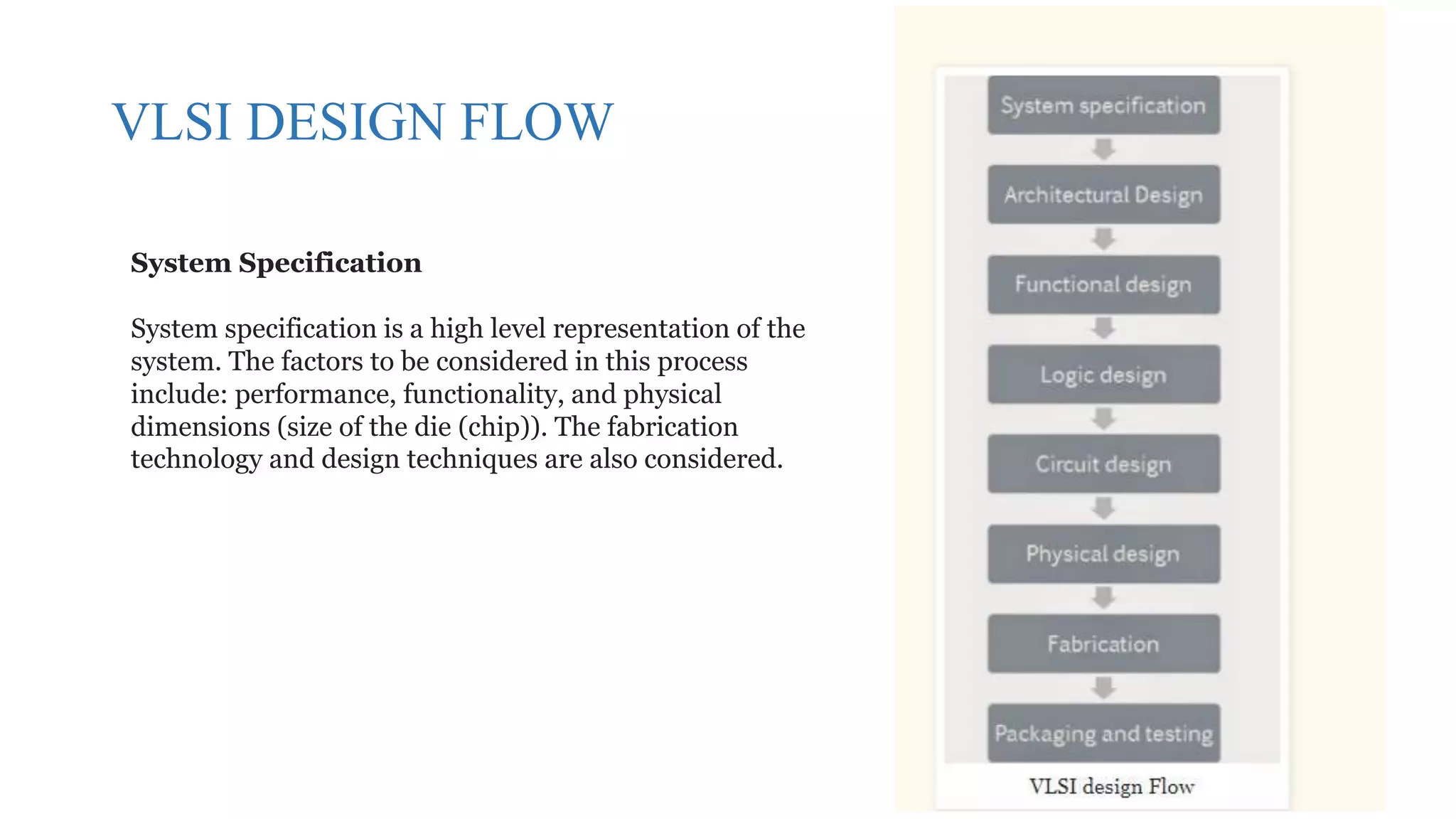
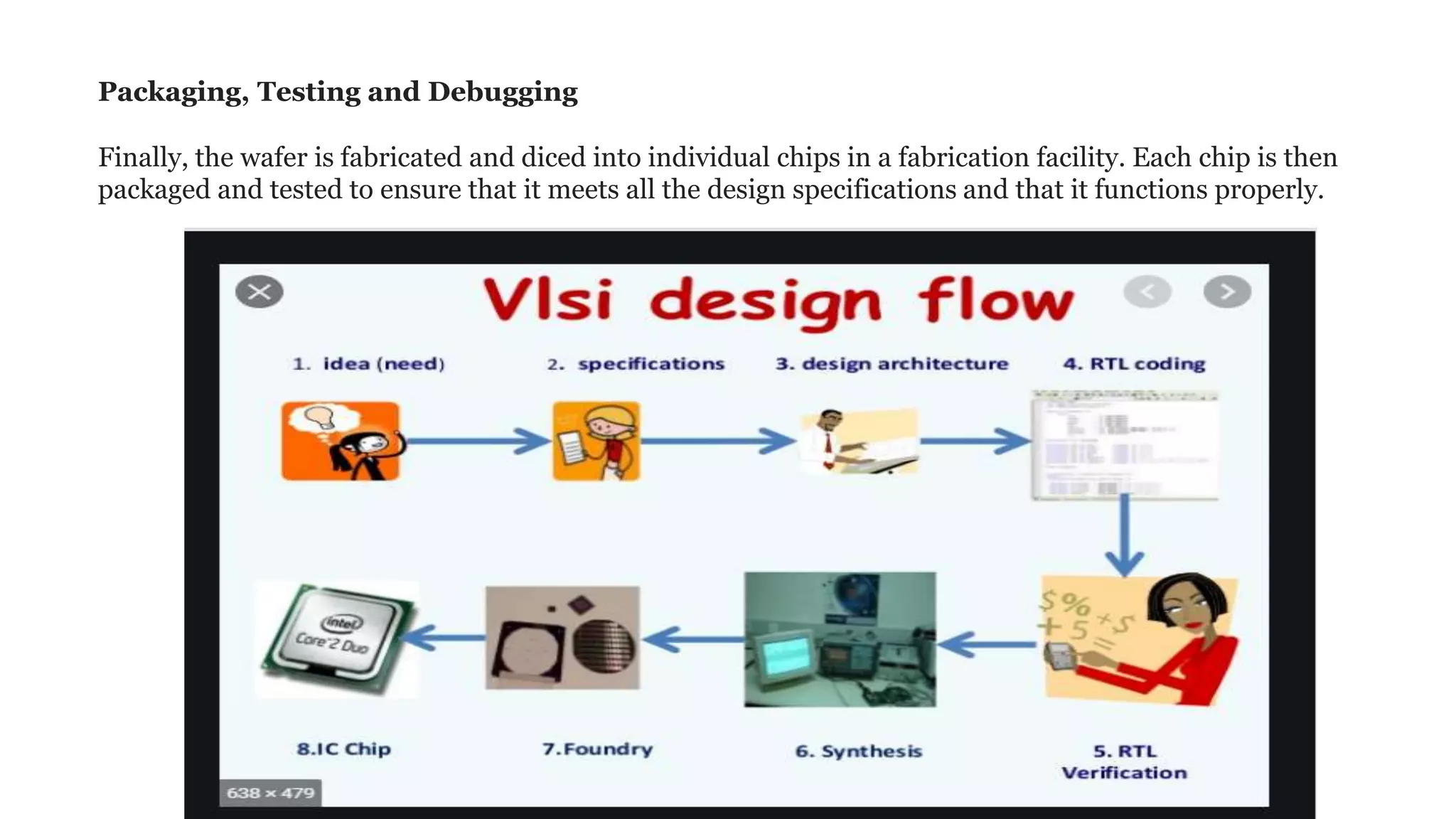
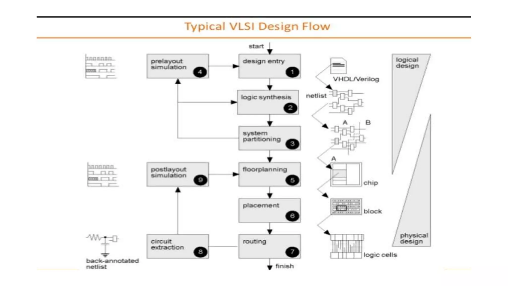
VLSI DESIGN FLOW
System Specification
System specification is a high level representation of the
system. The factors to be considered in this process
include: performance, functionality, and physical
dimensions (size of the die (chip)). The fabrication
technology and design techniques are also considered.
Architectural Design
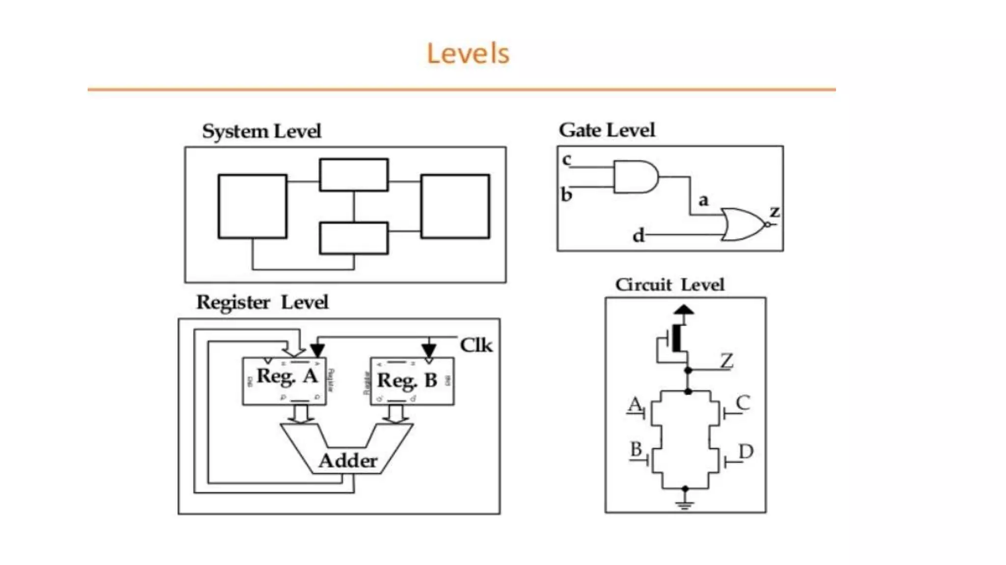
The basic architecture of the system is designed in this step. This includes, such decisions as RISC (Reduced
Instruction Set Computer) versus CISC (Complex Instruction Set Computer), number of ALUs, Floating
Point units, number and structure of pipelines, and size of caches among others.
Behavioural or Functional Design
Main functional units of the system are identified. This also identifies the interconnect requirements
between the units. The area, power, and other parameters of each unit are estimated.
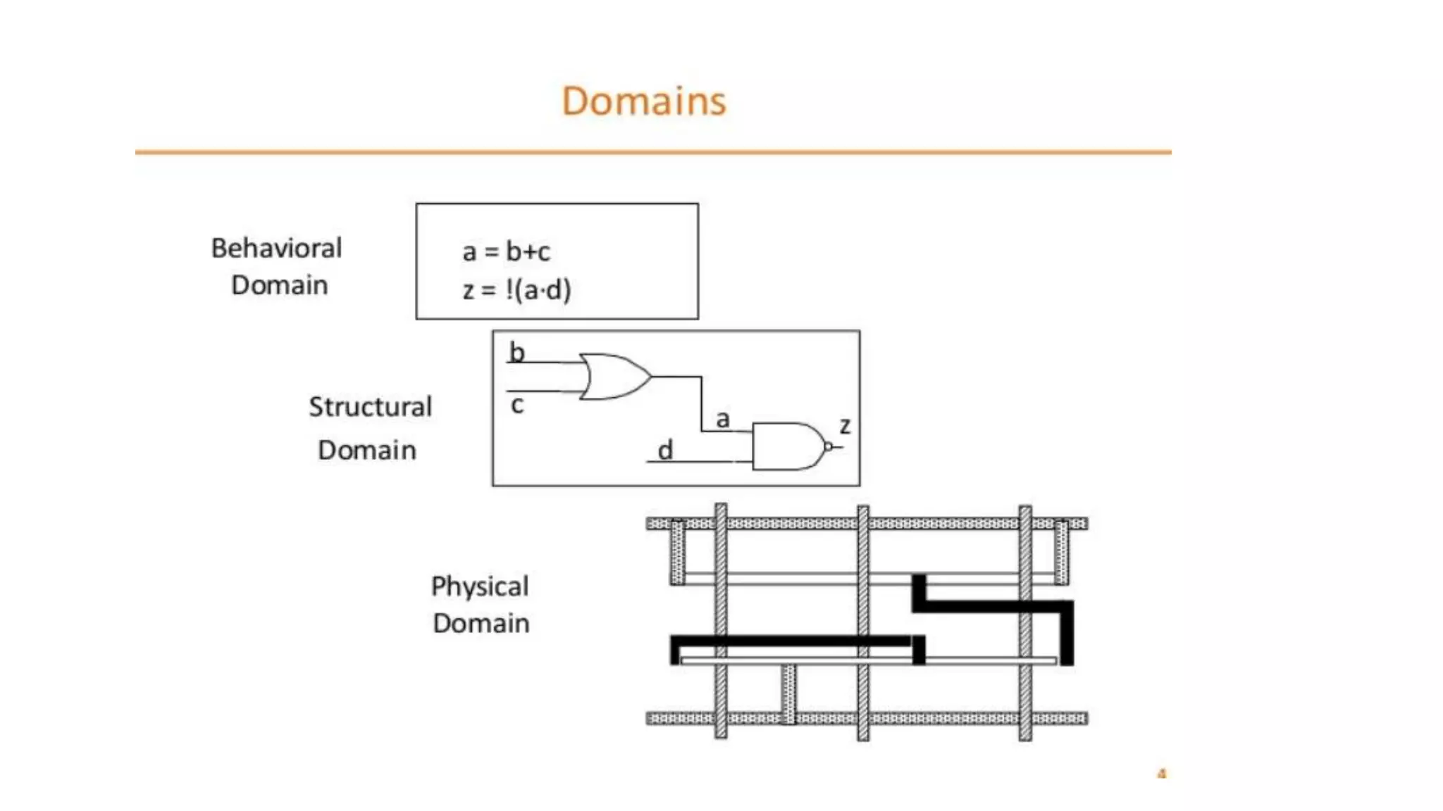
The behavioral aspects of the system are considered without implementation specific information. For
example, it may specify that a multiplication is required, but exactly in which mode such multiplication may
be executed is not specified. We may use a variety of multiplication hardware depending on the speed and
word size requirements. The key idea is to specify behavior, in terms of input, output and timing of each
unit, without specifying its internal structure.
Logic Design
•In this step the control flow, word widths, register allocation, arithmetic operations, and logic
operations of the design that represent the functional design are derived and tested.
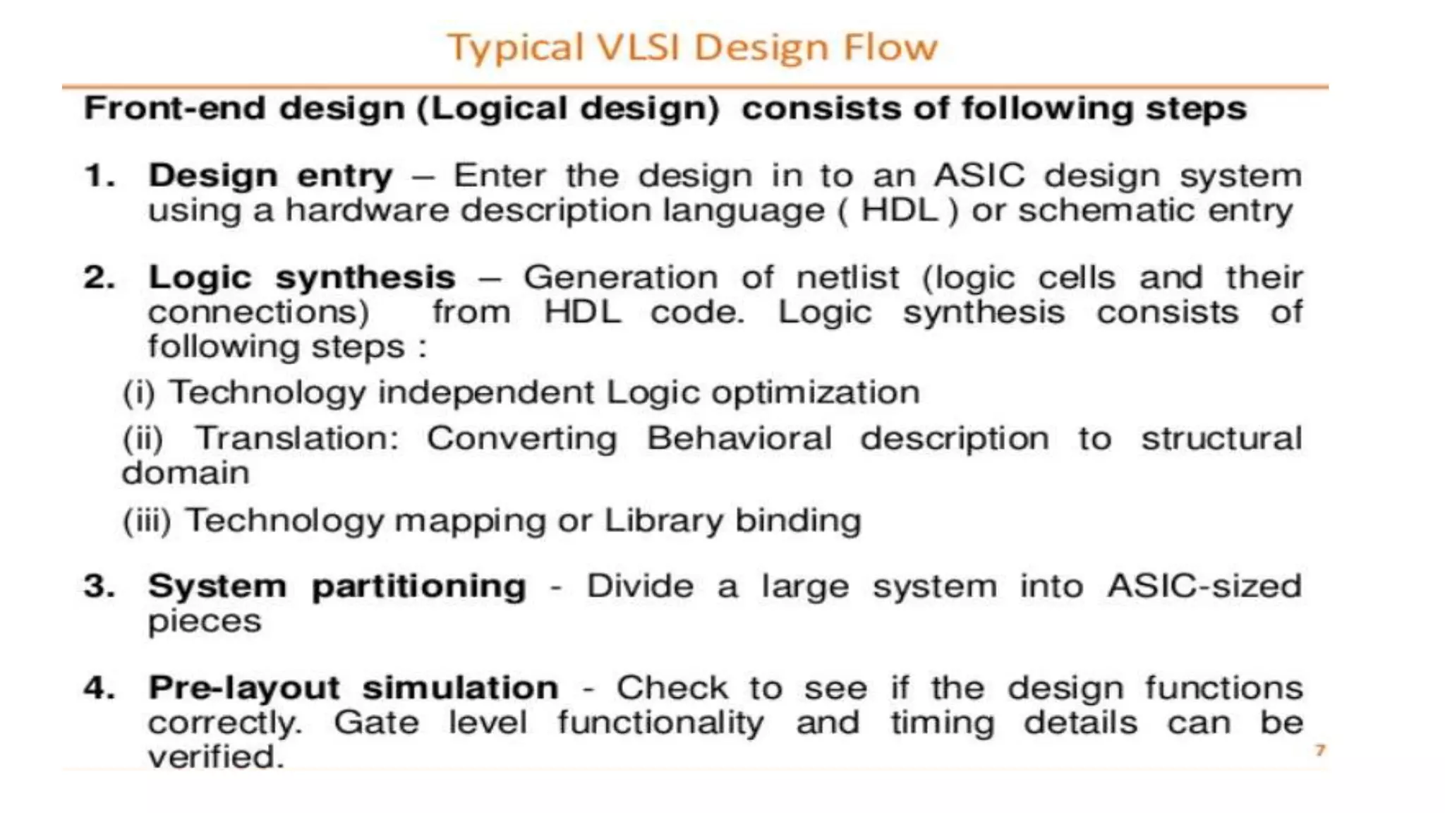
• This description is called Register Transfer Level (RTL) description. RTL is expressed in a
Hardware Description Language (HDL), such as VHDL or Verilog. This description can be used in
simulation and verification. This description consists of Boolean expressions and timing
information.
Circuit Design
The purpose of circuit design is to develop a circuit representation based on the logic design. The
Boolean expressions are converted into a circuit representation by taking into consideration the
speed and power requirements of the original design. Circuit Simulation is used to verify the
correctness and timing of each component.
The circuit design is usually expressed in a detailed circuit diagram. This diagram shows the
circuit elements (cells, macros, gates, transistors) and interconnection between these elements.
This representation is also called a netlist.
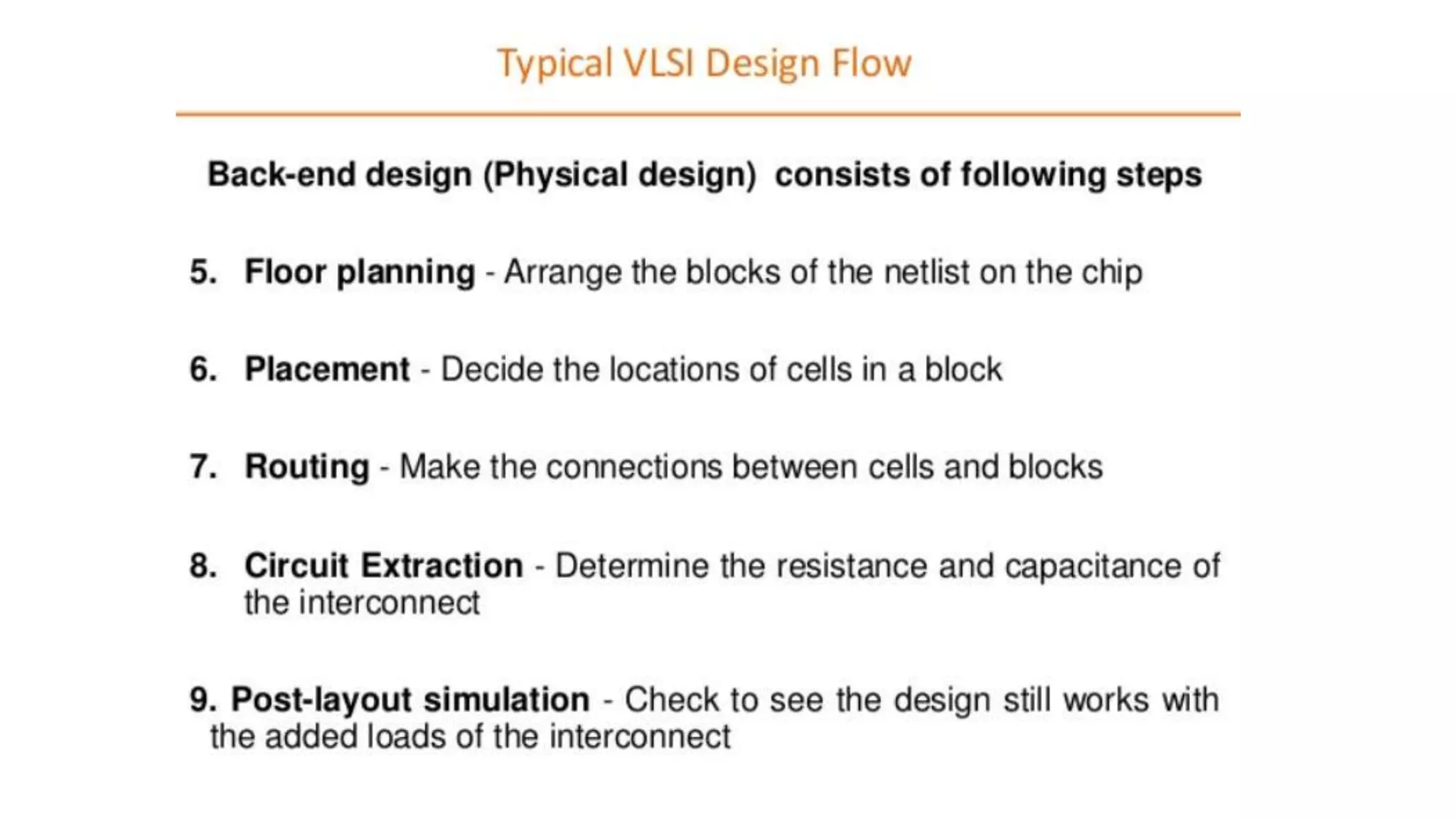
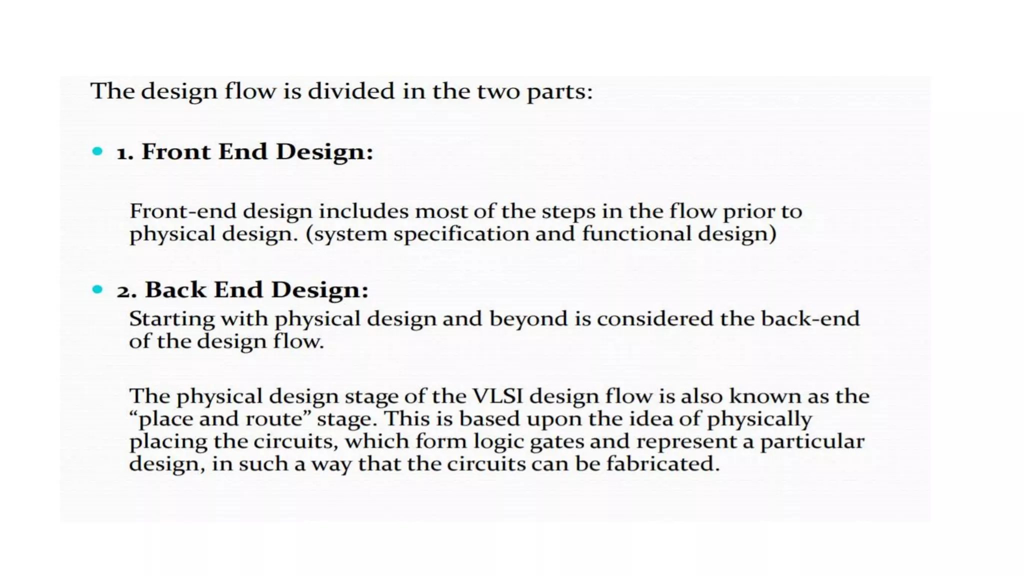
Physical Design
Circuit representation (or netlist) is converted into a geometric representation.
This geometric representation of a circuit is called a layout. Layout is created by converting each logic
component (cells, macros, gates, transistors) into a geometric representation (specific shapes in multiple
layers), which perform the intended logic function of the corresponding component. Connections between
different components are also expressed as geometric patterns typically lines in multiple layers.
Physical design can be completely or partially automated and layout can be generated directly from netlist
by Layout Synthesis tools. Layout synthesis tools, while fast, do have an area and performance penalty, which
limit their use to some designs.
Physical design is a very complex process and therefore it is usually broken down into various sub-steps.
Various verification and validation checks are performed on the layout during physical design.
Fabrication
After layout and verification, the design is ready for fabrication. Since layout data is typically sent to
fabrication on a tape, the event of release of data is called Tape Out. Layout data is converted (or
fractured) into photo-lithographic masks, one for each layer.
The fabrication process consists of several steps involving deposition, and diffusion of various materials
on the wafer. During each step one mask is used. Several dozen masks may be used to complete the
fabrication process.
Packaging, Testing and Debugging
Finally, the wafer is fabricated and diced into individual chips in a fabrication facility. Each chip is then
packaged and tested to ensure that it meets all the design specifications and that it functions properly.
VLSI design flow.pptx

VLSI design flow.pptx

  • 1.
    UNIT II VLSI CIRUITDESIGN PROCESS  VLSI Design Flow  MOS Layers  Stick Diagrams  Design Rules and Layout  Lamda (λ) based design rules for wires, contacts and Transistors  Layout Diagrams for NMOS and CMOS Inverters and Gates  Scaling of MOS circuits
  • 2.
    VLSI DESIGN FLOW SystemSpecification System specification is a high level representation of the system. The factors to be considered in this process include: performance, functionality, and physical dimensions (size of the die (chip)). The fabrication technology and design techniques are also considered.
  • 3.
    Architectural Design The basicarchitecture of the system is designed in this step. This includes, such decisions as RISC (Reduced Instruction Set Computer) versus CISC (Complex Instruction Set Computer), number of ALUs, Floating Point units, number and structure of pipelines, and size of caches among others. Behavioural or Functional Design Main functional units of the system are identified. This also identifies the interconnect requirements between the units. The area, power, and other parameters of each unit are estimated. The behavioral aspects of the system are considered without implementation specific information. For example, it may specify that a multiplication is required, but exactly in which mode such multiplication may be executed is not specified. We may use a variety of multiplication hardware depending on the speed and word size requirements. The key idea is to specify behavior, in terms of input, output and timing of each unit, without specifying its internal structure.
  • 4.
    Logic Design •In thisstep the control flow, word widths, register allocation, arithmetic operations, and logic operations of the design that represent the functional design are derived and tested. • This description is called Register Transfer Level (RTL) description. RTL is expressed in a Hardware Description Language (HDL), such as VHDL or Verilog. This description can be used in simulation and verification. This description consists of Boolean expressions and timing information. Circuit Design The purpose of circuit design is to develop a circuit representation based on the logic design. The Boolean expressions are converted into a circuit representation by taking into consideration the speed and power requirements of the original design. Circuit Simulation is used to verify the correctness and timing of each component. The circuit design is usually expressed in a detailed circuit diagram. This diagram shows the circuit elements (cells, macros, gates, transistors) and interconnection between these elements. This representation is also called a netlist.
  • 5.
    Physical Design Circuit representation(or netlist) is converted into a geometric representation. This geometric representation of a circuit is called a layout. Layout is created by converting each logic component (cells, macros, gates, transistors) into a geometric representation (specific shapes in multiple layers), which perform the intended logic function of the corresponding component. Connections between different components are also expressed as geometric patterns typically lines in multiple layers. Physical design can be completely or partially automated and layout can be generated directly from netlist by Layout Synthesis tools. Layout synthesis tools, while fast, do have an area and performance penalty, which limit their use to some designs. Physical design is a very complex process and therefore it is usually broken down into various sub-steps. Various verification and validation checks are performed on the layout during physical design. Fabrication After layout and verification, the design is ready for fabrication. Since layout data is typically sent to fabrication on a tape, the event of release of data is called Tape Out. Layout data is converted (or fractured) into photo-lithographic masks, one for each layer. The fabrication process consists of several steps involving deposition, and diffusion of various materials on the wafer. During each step one mask is used. Several dozen masks may be used to complete the fabrication process.
  • 6.
    Packaging, Testing andDebugging Finally, the wafer is fabricated and diced into individual chips in a fabrication facility. Each chip is then packaged and tested to ensure that it meets all the design specifications and that it functions properly.