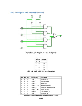
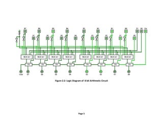
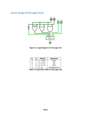
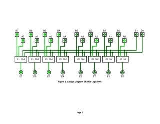
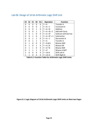
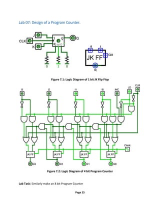
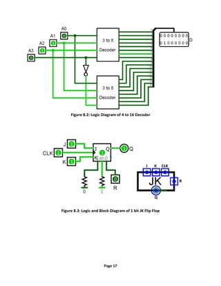
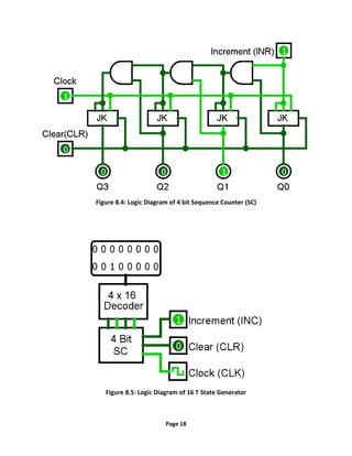
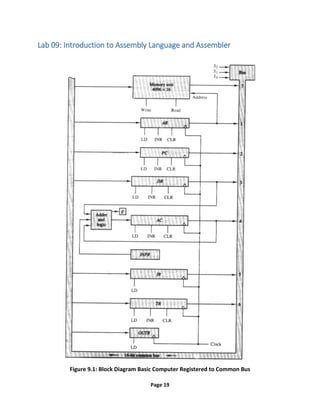
The document is a lab manual for the Computer Architecture and Organization course at the International Islamic University, Islamabad, focusing on object-oriented programming in C++. It includes practical lab exercises on microprocessor design, programming, and assembly language, outlining the objectives, methodologies, and rubrics for evaluation. Each lab covers specific design tasks, such as creating adders, counters, and implementing assembly language programs.

![Page 20
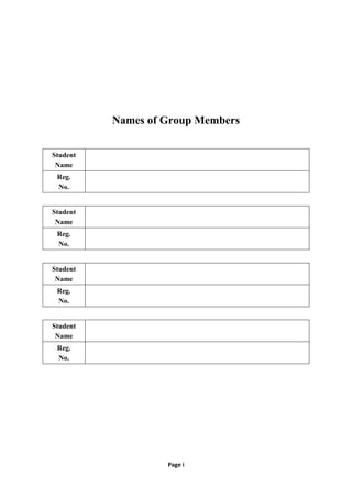
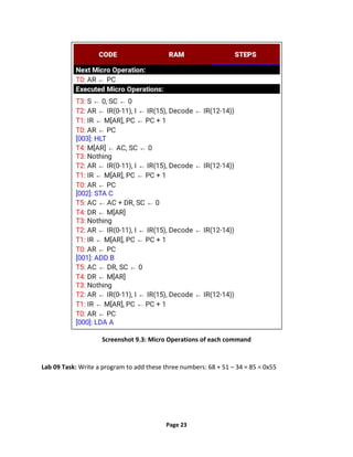
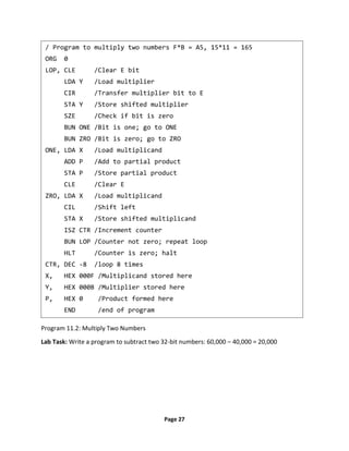
Memory Reference Instructions
Hexadecimal Code
Symbol I = 0 I = 1 Description
AND 0xxx 8xxx AND memory word to AC
AC ← AC & M[AR]
ADD 1xxx 9xxx Add memory word to AC
AC ← AC & M[AR] , E ← Cout
LDA 2xxx Axxx Load memory word to AC
AC ← M[AR]
STA 3xxx Bxxx Store content of AC in memory
M[AR] ← AC
BUN 4xxx Cxxx Branch unconditionally
PC ← AR
BSA 5xxx Dxxx Branch and save return address
M[AR] ← PC , PC ← AR + 1
ISZ 6xxx Exxx Increment and skip if zero
M[AR] ← M[AR] + 1
If( M[AR] + 1=0 ) then PC ← PC + 1
Register Reference Instructions
CLA 7800 Clear AC
CLE 7400 Clear E
CMA 7200 Complement AC
CME 7100 Complement E
CIR 7080 Circulate right AC and E
CIL 7040 Circulate left AC and E
INC 7020 Increment AC
SPA 7010 Skip next instruction if AC positive
SNA 7008 Skip next instruction if AC negative
SZA 7004 Skip next instruction if AC zero
SZE 7002 Skip next instruction if E is 0
HLT 7001 Halt Computer
IO Instructions
INP F800 Input character to AC
OUT F400 Output character from AC
SKI F200 Skip on input flag
SKO F100 Skip on output flag
ION F080 Interrupt on
IOF F040 Interrupt off
TABLE 9.1: Basic Computer Instructions](https://image.slidesharecdn.com/labmanualcomputerarchitecture-240507045620-c6184626/85/Lab-Manual-Computer-Organization-and-Architecture-25-320.jpg)
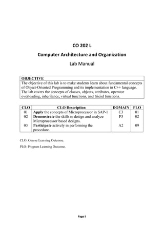
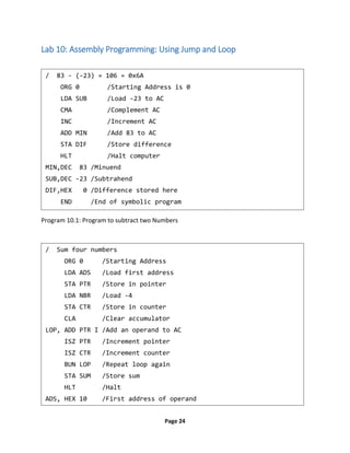
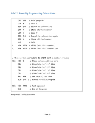
![Page 21
Instruction T State Micro Operation
Instruction
Cycle
T0 AR←PC
T1 IR ← M[AR] , AR ← PC + 1
T2 AR ← IR(0-11) , I ← IR(15) , Decode ← IR(12-14)
Register Reference Instructions
CLA T3 AC ← 0 , SC ← 0
CLE T3 E ← 0 , SC ← 0
CMA T3 AC ← AC_Bar , SC ← 0
CME T3 E ← E_Bar , SC ← 0
CIR T3 AC ← shr AC , AC(15) ← E , E ← AC(0) , SC ← 0
CIL T3 AC ← shl AC , AC(0) ← E , E ← AC(15) , SC ← 0
INC T3 AC ← AC + 1, SC ← 0
SPA T3 if(AC(15)=0) then PC ← PC + 1 , SC ← 0
SNA T3 if(AC(15)=1) then PC ← PC + 1 , SC ← 0
SZA T3 if(AC=0) then PC ← PC + 1, SC ← 0
SZE T3 if(E=0) then PC ← PC + 1 , SC ← 0
HLT T3 S ← 0 , SC ← 0
Memory Reference Instructions
AND T3
T4
T5
If(I-=1) AR ← M[AR] else “do nothing”
DR ← M[AR]
AC ← AC & DR, 0 ← SC
ADD T3
T4
T5
If(I-=1) AR ← M[AR] else “do nothing”
DR ← M[AR]
AC ← AC + DR , 0 ← SC
LDA T3
T4
T5
If(I-=1) AR ← M[AR] else “do nothing”
DR ← M[AR]
AR ← DR , 0 ← SC
STA T3
T4
If(I-=1) AR ← M[AR] else “do nothing”
M[AR] ← AC , 0 ← SC
BUN T3
T4
If(I-=1) AR ← M[AR] else “do nothing”
PC ← AR , 0 ← SC
BSA T3
T4
T5
If(I-=1) AR ← M[AR] else “do nothing”
M[AR] ← PC , AR← AR + 1
PC ← AR , 0 ← SC
ISZ T3
T4
T5
T6
If(I-=1) AR ← M[AR] else “do nothing”
DR ← M[AR]
DR ← DR + 1
M[AR] ← DR , if(DR=0) then PC ← PC + 1 , 0 ← SC
TABLE 9.2: Basic Computer Instructions with T States](https://image.slidesharecdn.com/labmanualcomputerarchitecture-240507045620-c6184626/85/Lab-Manual-Computer-Organization-and-Architecture-26-320.jpg)


![20230809133941_[11] 27 Datapath Introduction_1 NEW.pptx](https://cdn.slidesharecdn.com/ss_thumbnails/202308091339411127datapathintroduction1new-251108061328-e0605b9a-thumbnail.jpg?width=640&height=640&fit=bounds)