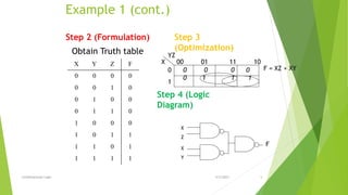
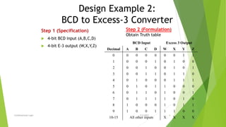
Lecture 8 Agenda:
 Combinational Circuits
 Design Procedure
 Half, Full and Parallel Adder
 Half and Full Subtractor
Combinational circuits
 Consists of logic gates whose
output depends on only the
present input.
 Example: Adder
1
0
+________
1
Sequential circuits
 Consists of logic gates + storage
elements. Output depends on inputs
and the state of the storage elements
or previous outputs.
 Example: Counter
 4+1 5
 3+14
5/2/2023
Combinational Logic 2
• Logic circuits for digital systems may be….
Introduction
Sequential circuits are the building blocks of digital systems
and will be discussed in next chapter.
Design Procedure
 Starts from the specification of the problem, which leads
to the truth table. Using the output values of truth table,
the logic equation and simplified using K maps, or
Algebraic manipulation. The equation of the output
functions, the corresponding circuit is found. The process
is shown in Figure:
5/2/2023
Logic Diagram
Verification Specification
Optimization
K-Map Boolean Algebra
Formulation
Truth Table Boolean Equation
Specification
Goal Functionality
Combinational Logic 3
Example 1
 Design a circuit that has a 3-bit input and a single
output (F) specified as follows:
• F = 0, when the input is less than (5)
• F = 1, otherwise
Solution:
 Step 1 (Specification):
• Label the inputs (3 bits) as X, Y, Z
• X is the most significant bit, Z is the least significant bit
• The output (1 bit) is F:
• F = 1  (101)2, (110)2, (111)2
• F = 0  other inputs
5/2/2023
Combinational Logic 4
Step 2 (Formulation)
Obtain Truth table
X Y Z F
0 0 0 0
0 0 1 0
0 1 0 0
0 1 1 0
1 0 0 0
1 0 1 1
1 1 0 1
1 1 1 1
X
YZ
0
1
00 01 11 10
0 0 0 0
0 1 1 1
Step 3
(Optimization)
F = XZ + XY
X
Z
X
Y
F
Example 1 (cont.)
Step 4 (Logic
Diagram)
5/2/2023
Combinational Logic 5
BCD Input Excess 3 Output
Decimal A B C D W X Y Z
0 0 0 0 0 0 0 1 1
1 0 0 0 1 0 1 0 0
2 0 0 1 0 0 1 0 1
3 0 0 1 1 0 1 1 0
4 0 1 0 0 0 1 1 1
5 0 1 0 1 1 0 0 0
6 0 1 1 0 1 0 0 1
7 0 1 1 1 1 0 1 0
8 1 0 0 0 1 0 1 1
9 1 0 0 1 1 1 0 0
10-15 All other inputs X X X X
Step 1 (Specification)
 4-bit BCD input (A,B,C,D)
 4-bit E-3 output (W,X,Y,Z)
Design Example 2:
BCD to Excess-3 Converter
Step 2 (Formulation)
Obtain Truth table
5/2/2023
Combinational Logic 6
Example 2 (cont.)
Step 3
(Optimization)
Step 4 (Logic
Diagram)
5/2/2023
Combinational Logic 7
Exercise Problems
Problem 4.4
Design a combinational circuit with three inputs and one output.
(a) The output is 1 when the binary value of the inputs is less than 3. The output is 0 otherwise.
(b) The output is 1 when the binary value of the inputs is an even number.
Problem 4.5
Design a combinational circuit with three inputs, x , y , and z , and three outputs, A, B , and C.
When the binary input is 0, 1, 2, or 3, the binary output is one greater than the input. When the
binary input is 4, 5, 6, or 7, the binary output is two less than the input.
Problem 4.6
A majority circuit is a combinational circuit whose output is equal to 1 if the input variables
have more 1’s than 0’s. The output is 0 otherwise. Design a 3-input majority circuit by finding the
circuit’s truth table, Boolean equation, and a logic diagram.
Exercise Problems
Problem 4.7
Design a combinational circuit that converts a four-bit Gray code to a four bit binary
number. Implement the circuit with exclusive-OR gates.
BINARY ADDER–SUBTRACTOR
0 + 0 = 0
0 + 1 = 1
1 + 0 = 1
1 + 1 = 10
 A combinational circuit that performs the addition of two bits is called a half
adder .
 One that performs the addition of three bits is a full adder .
 half adders + half adders = full adder.
5/2/2023
Combinational Logic 10
Half Adder
5/2/2023
Step 3
(Optimization)
Step 4 (Logic
Diagram)
Step 1
(Specification)
Step 2 (Formulation)
Combinational Logic 11
Full Adder
5/2/2023
Step 1
(Specification)
Step 2 (Formulation)
Combinational Logic 12
5/2/2023
Full Adder
Step 3
(Optimization)
Step 4 (Logic
Diagram)
Combinational Logic 13
5/2/2023
Full Adder = Two Half Adder
Combinational Logic 14
Half Sub tractor
5/2/2023
Step 3
(Optimization) Step 4 (Logic
Diagram)
Step 1
(Specification)
Step 2 (Formulation)
Combinational Logic 15
Full Sub tractor
5/2/2023
Step 1
(Specification)
Step 2 (Formulation)
X-Y-Z
Combinational Logic 16
5/2/2023
Full Sub tractor
Step 3
(Optimization) Step 4 (Logic
Diagram)
Combinational Logic 17
5/2/2023
Full Sub tractor = Two Half Sub tractor
Implementation of full-subtractor with two half subtractor and an OR gate
Combinational Logic 18
Exercise Problems
Problem 4.11
Using four half-adders,
(a) Design a full adder circuit incrementer. (A circuit that adds one to a four bit
binary number.)
(b) Design a four-bit combinational decrementer (a circuit that subtracts 1 from a four bit
binary number).
Problem 4.21
Design a combinational circuit that compares two 4-bit numbers to check if they are equal. The
circuit output is equal to 1 if the two numbers are equal and 0 otherwise.

Lecture 8.pptx

  • 1.
    Lecture 8 Agenda: Combinational Circuits  Design Procedure  Half, Full and Parallel Adder  Half and Full Subtractor
  • 2.
    Combinational circuits  Consistsof logic gates whose output depends on only the present input.  Example: Adder 1 0 +________ 1 Sequential circuits  Consists of logic gates + storage elements. Output depends on inputs and the state of the storage elements or previous outputs.  Example: Counter  4+1 5  3+14 5/2/2023 Combinational Logic 2 • Logic circuits for digital systems may be…. Introduction Sequential circuits are the building blocks of digital systems and will be discussed in next chapter.
  • 3.
    Design Procedure  Startsfrom the specification of the problem, which leads to the truth table. Using the output values of truth table, the logic equation and simplified using K maps, or Algebraic manipulation. The equation of the output functions, the corresponding circuit is found. The process is shown in Figure: 5/2/2023 Logic Diagram Verification Specification Optimization K-Map Boolean Algebra Formulation Truth Table Boolean Equation Specification Goal Functionality Combinational Logic 3
  • 4.
    Example 1  Designa circuit that has a 3-bit input and a single output (F) specified as follows: • F = 0, when the input is less than (5) • F = 1, otherwise Solution:  Step 1 (Specification): • Label the inputs (3 bits) as X, Y, Z • X is the most significant bit, Z is the least significant bit • The output (1 bit) is F: • F = 1  (101)2, (110)2, (111)2 • F = 0  other inputs 5/2/2023 Combinational Logic 4
  • 5.
    Step 2 (Formulation) ObtainTruth table X Y Z F 0 0 0 0 0 0 1 0 0 1 0 0 0 1 1 0 1 0 0 0 1 0 1 1 1 1 0 1 1 1 1 1 X YZ 0 1 00 01 11 10 0 0 0 0 0 1 1 1 Step 3 (Optimization) F = XZ + XY X Z X Y F Example 1 (cont.) Step 4 (Logic Diagram) 5/2/2023 Combinational Logic 5
  • 6.
    BCD Input Excess3 Output Decimal A B C D W X Y Z 0 0 0 0 0 0 0 1 1 1 0 0 0 1 0 1 0 0 2 0 0 1 0 0 1 0 1 3 0 0 1 1 0 1 1 0 4 0 1 0 0 0 1 1 1 5 0 1 0 1 1 0 0 0 6 0 1 1 0 1 0 0 1 7 0 1 1 1 1 0 1 0 8 1 0 0 0 1 0 1 1 9 1 0 0 1 1 1 0 0 10-15 All other inputs X X X X Step 1 (Specification)  4-bit BCD input (A,B,C,D)  4-bit E-3 output (W,X,Y,Z) Design Example 2: BCD to Excess-3 Converter Step 2 (Formulation) Obtain Truth table 5/2/2023 Combinational Logic 6
  • 7.
    Example 2 (cont.) Step3 (Optimization) Step 4 (Logic Diagram) 5/2/2023 Combinational Logic 7
  • 8.
    Exercise Problems Problem 4.4 Designa combinational circuit with three inputs and one output. (a) The output is 1 when the binary value of the inputs is less than 3. The output is 0 otherwise. (b) The output is 1 when the binary value of the inputs is an even number. Problem 4.5 Design a combinational circuit with three inputs, x , y , and z , and three outputs, A, B , and C. When the binary input is 0, 1, 2, or 3, the binary output is one greater than the input. When the binary input is 4, 5, 6, or 7, the binary output is two less than the input. Problem 4.6 A majority circuit is a combinational circuit whose output is equal to 1 if the input variables have more 1’s than 0’s. The output is 0 otherwise. Design a 3-input majority circuit by finding the circuit’s truth table, Boolean equation, and a logic diagram.
  • 9.
    Exercise Problems Problem 4.7 Designa combinational circuit that converts a four-bit Gray code to a four bit binary number. Implement the circuit with exclusive-OR gates.
  • 10.
    BINARY ADDER–SUBTRACTOR 0 +0 = 0 0 + 1 = 1 1 + 0 = 1 1 + 1 = 10  A combinational circuit that performs the addition of two bits is called a half adder .  One that performs the addition of three bits is a full adder .  half adders + half adders = full adder. 5/2/2023 Combinational Logic 10
  • 11.
    Half Adder 5/2/2023 Step 3 (Optimization) Step4 (Logic Diagram) Step 1 (Specification) Step 2 (Formulation) Combinational Logic 11
  • 12.
    Full Adder 5/2/2023 Step 1 (Specification) Step2 (Formulation) Combinational Logic 12
  • 13.
    5/2/2023 Full Adder Step 3 (Optimization) Step4 (Logic Diagram) Combinational Logic 13
  • 14.
    5/2/2023 Full Adder =Two Half Adder Combinational Logic 14
  • 15.
    Half Sub tractor 5/2/2023 Step3 (Optimization) Step 4 (Logic Diagram) Step 1 (Specification) Step 2 (Formulation) Combinational Logic 15
  • 16.
    Full Sub tractor 5/2/2023 Step1 (Specification) Step 2 (Formulation) X-Y-Z Combinational Logic 16
  • 17.
    5/2/2023 Full Sub tractor Step3 (Optimization) Step 4 (Logic Diagram) Combinational Logic 17
  • 18.
    5/2/2023 Full Sub tractor= Two Half Sub tractor Implementation of full-subtractor with two half subtractor and an OR gate Combinational Logic 18
  • 19.
    Exercise Problems Problem 4.11 Usingfour half-adders, (a) Design a full adder circuit incrementer. (A circuit that adds one to a four bit binary number.) (b) Design a four-bit combinational decrementer (a circuit that subtracts 1 from a four bit binary number). Problem 4.21 Design a combinational circuit that compares two 4-bit numbers to check if they are equal. The circuit output is equal to 1 if the two numbers are equal and 0 otherwise.