SlideShare a Scribd company logo
RISE OF THE NANOWIRE TRANSISTOR
Compound-semiconductor nanowire to keep smartphones charged longer
Chalamaneni Jeevan Prasad (154M1A0419)
Department of E.C.E, VEMU Institute of Technology, Chittoor 517124
ABSTRACT
1. Superior gate control (minimize channel effects).
2. High drive current.
3. Less sensitive to process variations.
4. Improved transport property.
5. Ultimate limit on the current trend of down
Scaling transistors and integrated circuits to
achieve faster speeds and lower power consumption
INTRODUCTION
NANO WIRE
Nanowires are microscopic wires that have a
width measured in Nano meters. Typically their
width ranges from forty to fifty Nano meters, but
their length is not so limited. Since they can be
lengthened by simply attaching more wires end
to end or just by growing them longer, they can
be as long as desired.
FEATURES
SIZE IMPRESSION ON NANO WIRE
REFERENCES
CONCLUSION
RESULT
Reduction in lattice thermal conductance as high as
30% obtained by 20% atom removal. Weak material
depend Si & Ge nanowire show similar reduction.
Node reduction in lattice thermal conductance.
RTDs is much faster than any other conventional trans.
Very good rectifier low leakage current. Much research
needs to be done to improve the output power and also
to integrate them with conventional transistors.
Volume inversion dominant until dnw=4nm. Surface phonon
and back scattering dominant below dnw=4nm.
We cherish our smartphones for delivering
entertainment and information on the go but their
need for daily charging is a problem. So when new
smartphone models come on the market with
Microprocessors based on the latest foundry
process, the increase in the number of transistors
in the chips should be balanced by a reduction in
the power.
https://ieeexplore.ieee.org/abstract/document/4419093

GSDSAT VI 
Sung Dae Suk, et al., “Investigation of nanowire size dependency on
TSNWFET,” IEDM 2007, pp. 891-894.
Kyoung Hwan Yeo, et al., “Gate-All-Around (GAA) Twin Silicon
Nanowire MOSFET (TSNWFET),” IEDM 2006.
▪ At around 10 nanometres from the interface, the quality
of the material is very good, so we can grow the. Channel
layers.
▪ The total thickness for the layers bridging the difference in
lattice spacing is just 150 nm, compared with roughly 1μm.
▪ Traditional buffer layers, meaning less material, lower
costs, and faster production.
▪ It avoids many complications of crystal growth.
▪ The nanowire devices also yielded a trans conductance of
1,057 μS/μm, which is a record for electron-transporting
germanium nanowire FETs.

More Related Content

What's hot

3D or Tri-gate transistors
3D or Tri-gate transistors3D or Tri-gate transistors
3D or Tri-gate transistors
Karanvir Singh
 
TRI GATE TRANSISTOR
TRI GATE TRANSISTORTRI GATE TRANSISTOR
TRI GATE TRANSISTORVINOD MAURYA
 
SEBA KMT MFM5 1 Cable Sheath Testing, Fault Prelocation & Pinpointing
SEBA KMT MFM5 1 Cable Sheath Testing, Fault Prelocation & PinpointingSEBA KMT MFM5 1 Cable Sheath Testing, Fault Prelocation & Pinpointing
SEBA KMT MFM5 1 Cable Sheath Testing, Fault Prelocation & Pinpointing
Thorne & Derrick International
 
Parallel wire Technique in CTO PCI
Parallel wire Technique in CTO PCIParallel wire Technique in CTO PCI
Parallel wire Technique in CTO PCI
wasimcardio21
 
Sushant
SushantSushant
Finfet; My 3rd PPT in clg
Finfet; My 3rd PPT in clgFinfet; My 3rd PPT in clg
Finfet; My 3rd PPT in clgARUNASUJITHA
 
Introduction to FinFET
Introduction to FinFETIntroduction to FinFET
Introduction to FinFET
ManishKenchi
 
eDRAM Cells using FinFET Technology
eDRAM Cells using FinFET TechnologyeDRAM Cells using FinFET Technology
eDRAM Cells using FinFET Technology
Anupama K
 
22nm tri-gate technology
22nm tri-gate technology22nm tri-gate technology
22nm tri-gate technology
Arjun Challu
 
Visi fault™ visual fault locator
Visi fault™ visual fault locatorVisi fault™ visual fault locator
Visi fault™ visual fault locator
Fluke Networks
 
Finfet tech
Finfet techFinfet tech
Finfet tech
neela458
 
Minor report
Minor reportMinor report
Minor report
ShamimAhmed680298
 
Cutoff wavelength in optical fibre
Cutoff wavelength in optical fibreCutoff wavelength in optical fibre
Cutoff wavelength in optical fibre
home
 
Stringer machine
Stringer machineStringer machine
Fiber optics 2-3
Fiber optics 2-3Fiber optics 2-3
Fiber optics 2-3
grantlerc
 
Effective Elastic Properties of a Molecular Monolayer at a Metal Surface
Effective Elastic Properties of a Molecular Monolayer at a Metal SurfaceEffective Elastic Properties of a Molecular Monolayer at a Metal Surface
Effective Elastic Properties of a Molecular Monolayer at a Metal Surfacesummeronly
 
Cable Sniffer LV Cable Fault Locator - Operating Manual
Cable Sniffer LV Cable Fault Locator - Operating ManualCable Sniffer LV Cable Fault Locator - Operating Manual
Cable Sniffer LV Cable Fault Locator - Operating Manual
Thorne & Derrick International
 
G1303054353
G1303054353G1303054353
G1303054353
IOSR Journals
 
Acoustic sensors
Acoustic sensorsAcoustic sensors
Acoustic sensors
Shankar Sahni
 
Rm.naatchammai vlsi paper ppt
Rm.naatchammai vlsi paper pptRm.naatchammai vlsi paper ppt
Rm.naatchammai vlsi paper ppt
Naatchammai Ramanathan
 

What's hot (20)

3D or Tri-gate transistors
3D or Tri-gate transistors3D or Tri-gate transistors
3D or Tri-gate transistors
 
TRI GATE TRANSISTOR
TRI GATE TRANSISTORTRI GATE TRANSISTOR
TRI GATE TRANSISTOR
 
SEBA KMT MFM5 1 Cable Sheath Testing, Fault Prelocation & Pinpointing
SEBA KMT MFM5 1 Cable Sheath Testing, Fault Prelocation & PinpointingSEBA KMT MFM5 1 Cable Sheath Testing, Fault Prelocation & Pinpointing
SEBA KMT MFM5 1 Cable Sheath Testing, Fault Prelocation & Pinpointing
 
Parallel wire Technique in CTO PCI
Parallel wire Technique in CTO PCIParallel wire Technique in CTO PCI
Parallel wire Technique in CTO PCI
 
Sushant
SushantSushant
Sushant
 
Finfet; My 3rd PPT in clg
Finfet; My 3rd PPT in clgFinfet; My 3rd PPT in clg
Finfet; My 3rd PPT in clg
 
Introduction to FinFET
Introduction to FinFETIntroduction to FinFET
Introduction to FinFET
 
eDRAM Cells using FinFET Technology
eDRAM Cells using FinFET TechnologyeDRAM Cells using FinFET Technology
eDRAM Cells using FinFET Technology
 
22nm tri-gate technology
22nm tri-gate technology22nm tri-gate technology
22nm tri-gate technology
 
Visi fault™ visual fault locator
Visi fault™ visual fault locatorVisi fault™ visual fault locator
Visi fault™ visual fault locator
 
Finfet tech
Finfet techFinfet tech
Finfet tech
 
Minor report
Minor reportMinor report
Minor report
 
Cutoff wavelength in optical fibre
Cutoff wavelength in optical fibreCutoff wavelength in optical fibre
Cutoff wavelength in optical fibre
 
Stringer machine
Stringer machineStringer machine
Stringer machine
 
Fiber optics 2-3
Fiber optics 2-3Fiber optics 2-3
Fiber optics 2-3
 
Effective Elastic Properties of a Molecular Monolayer at a Metal Surface
Effective Elastic Properties of a Molecular Monolayer at a Metal SurfaceEffective Elastic Properties of a Molecular Monolayer at a Metal Surface
Effective Elastic Properties of a Molecular Monolayer at a Metal Surface
 
Cable Sniffer LV Cable Fault Locator - Operating Manual
Cable Sniffer LV Cable Fault Locator - Operating ManualCable Sniffer LV Cable Fault Locator - Operating Manual
Cable Sniffer LV Cable Fault Locator - Operating Manual
 
G1303054353
G1303054353G1303054353
G1303054353
 
Acoustic sensors
Acoustic sensorsAcoustic sensors
Acoustic sensors
 
Rm.naatchammai vlsi paper ppt
Rm.naatchammai vlsi paper pptRm.naatchammai vlsi paper ppt
Rm.naatchammai vlsi paper ppt
 

Similar to Final poster

Please read the following IEEE Spectrum articles and answer the quest.pdf
Please read the following IEEE Spectrum articles and answer the quest.pdfPlease read the following IEEE Spectrum articles and answer the quest.pdf
Please read the following IEEE Spectrum articles and answer the quest.pdf
fasttrackcomputersol
 
Nanoelectronics Final
Nanoelectronics FinalNanoelectronics Final
Nanoelectronics Finalshikha2510
 
W04406104107
W04406104107W04406104107
W04406104107
IJERA Editor
 
Gy3612471250
Gy3612471250Gy3612471250
Gy3612471250
IJERA Editor
 
Design of Nanoscale 3-T DRAM using FinFET
Design of Nanoscale 3-T DRAM using FinFETDesign of Nanoscale 3-T DRAM using FinFET
Design of Nanoscale 3-T DRAM using FinFET
IOSR Journals
 
REVIEW PAPER ON NEW TECHNOLOGY BASED NANOSCALE TRANSISTOR
REVIEW PAPER ON NEW TECHNOLOGY BASED NANOSCALE TRANSISTORREVIEW PAPER ON NEW TECHNOLOGY BASED NANOSCALE TRANSISTOR
REVIEW PAPER ON NEW TECHNOLOGY BASED NANOSCALE TRANSISTOR
msejjournal
 
REVIEW PAPER ON NEW TECHNOLOGY BASED NANOSCALE TRANSISTOR
REVIEW PAPER ON NEW TECHNOLOGY BASED NANOSCALE TRANSISTORREVIEW PAPER ON NEW TECHNOLOGY BASED NANOSCALE TRANSISTOR
REVIEW PAPER ON NEW TECHNOLOGY BASED NANOSCALE TRANSISTOR
msejjournal
 
Reconfigurable C and Ku band antenna Using Duelpatch
Reconfigurable C and Ku band antenna Using DuelpatchReconfigurable C and Ku band antenna Using Duelpatch
Reconfigurable C and Ku band antenna Using Duelpatch
IRJET Journal
 
A Comparative Performance Analysis of Copper on Chip and CNTFET Nano Intercon...
A Comparative Performance Analysis of Copper on Chip and CNTFET Nano Intercon...A Comparative Performance Analysis of Copper on Chip and CNTFET Nano Intercon...
A Comparative Performance Analysis of Copper on Chip and CNTFET Nano Intercon...
IRJET Journal
 
CNFET Technology
CNFET TechnologyCNFET Technology
CNFET Technology
Kunwar Rehan
 
Mlgnr interconnects with finfet driver optimized delay and power performance ...
Mlgnr interconnects with finfet driver optimized delay and power performance ...Mlgnr interconnects with finfet driver optimized delay and power performance ...
Mlgnr interconnects with finfet driver optimized delay and power performance ...
eSAT Publishing House
 
RBL paper _Design_of_MIGFET_based_junctionless_transistor
RBL paper _Design_of_MIGFET_based_junctionless_transistorRBL paper _Design_of_MIGFET_based_junctionless_transistor
RBL paper _Design_of_MIGFET_based_junctionless_transistorHema N
 
Dual-Diameter Variation –Immune CNFET-based 7T SRAM Cell
Dual-Diameter Variation –Immune CNFET-based 7T SRAM CellDual-Diameter Variation –Immune CNFET-based 7T SRAM Cell
Dual-Diameter Variation –Immune CNFET-based 7T SRAM Cell
Waqas Tariq
 
Kg3418451855
Kg3418451855Kg3418451855
Kg3418451855
IJERA Editor
 
Novel Microstrip Antenna Design for UWB
Novel Microstrip Antenna Design for UWBNovel Microstrip Antenna Design for UWB
Novel Microstrip Antenna Design for UWB
Anas Kadri
 
ZnO based transparent electronics
ZnO based transparent electronicsZnO based transparent electronics
ZnO based transparent electronics
cdtpv
 
CMOS VLSI design
CMOS VLSI designCMOS VLSI design
CMOS VLSI designRajan Kumar
 
SOTA.pptx
SOTA.pptxSOTA.pptx
Nanoscale Based Digital VLSI Circuits (1) - NEHA PATEL.pptx.pdf
Nanoscale Based Digital VLSI Circuits (1) - NEHA PATEL.pptx.pdfNanoscale Based Digital VLSI Circuits (1) - NEHA PATEL.pptx.pdf
Nanoscale Based Digital VLSI Circuits (1) - NEHA PATEL.pptx.pdf
batpad
 
Review of Fin FET Technology and Circuit Design Challenges
Review of Fin FET Technology and Circuit Design ChallengesReview of Fin FET Technology and Circuit Design Challenges
Review of Fin FET Technology and Circuit Design Challenges
IJERA Editor
 

Similar to Final poster (20)

Please read the following IEEE Spectrum articles and answer the quest.pdf
Please read the following IEEE Spectrum articles and answer the quest.pdfPlease read the following IEEE Spectrum articles and answer the quest.pdf
Please read the following IEEE Spectrum articles and answer the quest.pdf
 
Nanoelectronics Final
Nanoelectronics FinalNanoelectronics Final
Nanoelectronics Final
 
W04406104107
W04406104107W04406104107
W04406104107
 
Gy3612471250
Gy3612471250Gy3612471250
Gy3612471250
 
Design of Nanoscale 3-T DRAM using FinFET
Design of Nanoscale 3-T DRAM using FinFETDesign of Nanoscale 3-T DRAM using FinFET
Design of Nanoscale 3-T DRAM using FinFET
 
REVIEW PAPER ON NEW TECHNOLOGY BASED NANOSCALE TRANSISTOR
REVIEW PAPER ON NEW TECHNOLOGY BASED NANOSCALE TRANSISTORREVIEW PAPER ON NEW TECHNOLOGY BASED NANOSCALE TRANSISTOR
REVIEW PAPER ON NEW TECHNOLOGY BASED NANOSCALE TRANSISTOR
 
REVIEW PAPER ON NEW TECHNOLOGY BASED NANOSCALE TRANSISTOR
REVIEW PAPER ON NEW TECHNOLOGY BASED NANOSCALE TRANSISTORREVIEW PAPER ON NEW TECHNOLOGY BASED NANOSCALE TRANSISTOR
REVIEW PAPER ON NEW TECHNOLOGY BASED NANOSCALE TRANSISTOR
 
Reconfigurable C and Ku band antenna Using Duelpatch
Reconfigurable C and Ku band antenna Using DuelpatchReconfigurable C and Ku band antenna Using Duelpatch
Reconfigurable C and Ku band antenna Using Duelpatch
 
A Comparative Performance Analysis of Copper on Chip and CNTFET Nano Intercon...
A Comparative Performance Analysis of Copper on Chip and CNTFET Nano Intercon...A Comparative Performance Analysis of Copper on Chip and CNTFET Nano Intercon...
A Comparative Performance Analysis of Copper on Chip and CNTFET Nano Intercon...
 
CNFET Technology
CNFET TechnologyCNFET Technology
CNFET Technology
 
Mlgnr interconnects with finfet driver optimized delay and power performance ...
Mlgnr interconnects with finfet driver optimized delay and power performance ...Mlgnr interconnects with finfet driver optimized delay and power performance ...
Mlgnr interconnects with finfet driver optimized delay and power performance ...
 
RBL paper _Design_of_MIGFET_based_junctionless_transistor
RBL paper _Design_of_MIGFET_based_junctionless_transistorRBL paper _Design_of_MIGFET_based_junctionless_transistor
RBL paper _Design_of_MIGFET_based_junctionless_transistor
 
Dual-Diameter Variation –Immune CNFET-based 7T SRAM Cell
Dual-Diameter Variation –Immune CNFET-based 7T SRAM CellDual-Diameter Variation –Immune CNFET-based 7T SRAM Cell
Dual-Diameter Variation –Immune CNFET-based 7T SRAM Cell
 
Kg3418451855
Kg3418451855Kg3418451855
Kg3418451855
 
Novel Microstrip Antenna Design for UWB
Novel Microstrip Antenna Design for UWBNovel Microstrip Antenna Design for UWB
Novel Microstrip Antenna Design for UWB
 
ZnO based transparent electronics
ZnO based transparent electronicsZnO based transparent electronics
ZnO based transparent electronics
 
CMOS VLSI design
CMOS VLSI designCMOS VLSI design
CMOS VLSI design
 
SOTA.pptx
SOTA.pptxSOTA.pptx
SOTA.pptx
 
Nanoscale Based Digital VLSI Circuits (1) - NEHA PATEL.pptx.pdf
Nanoscale Based Digital VLSI Circuits (1) - NEHA PATEL.pptx.pdfNanoscale Based Digital VLSI Circuits (1) - NEHA PATEL.pptx.pdf
Nanoscale Based Digital VLSI Circuits (1) - NEHA PATEL.pptx.pdf
 
Review of Fin FET Technology and Circuit Design Challenges
Review of Fin FET Technology and Circuit Design ChallengesReview of Fin FET Technology and Circuit Design Challenges
Review of Fin FET Technology and Circuit Design Challenges
 

Recently uploaded

Student information management system project report ii.pdf
Student information management system project report ii.pdfStudent information management system project report ii.pdf
Student information management system project report ii.pdf
Kamal Acharya
 
ethical hacking-mobile hacking methods.ppt
ethical hacking-mobile hacking methods.pptethical hacking-mobile hacking methods.ppt
ethical hacking-mobile hacking methods.ppt
Jayaprasanna4
 
Halogenation process of chemical process industries
Halogenation process of chemical process industriesHalogenation process of chemical process industries
Halogenation process of chemical process industries
MuhammadTufail242431
 
Final project report on grocery store management system..pdf
Final project report on grocery store management system..pdfFinal project report on grocery store management system..pdf
Final project report on grocery store management system..pdf
Kamal Acharya
 
Quality defects in TMT Bars, Possible causes and Potential Solutions.
Quality defects in TMT Bars, Possible causes and Potential Solutions.Quality defects in TMT Bars, Possible causes and Potential Solutions.
Quality defects in TMT Bars, Possible causes and Potential Solutions.
PrashantGoswami42
 
DESIGN A COTTON SEED SEPARATION MACHINE.docx
DESIGN A COTTON SEED SEPARATION MACHINE.docxDESIGN A COTTON SEED SEPARATION MACHINE.docx
DESIGN A COTTON SEED SEPARATION MACHINE.docx
FluxPrime1
 
Vaccine management system project report documentation..pdf
Vaccine management system project report documentation..pdfVaccine management system project report documentation..pdf
Vaccine management system project report documentation..pdf
Kamal Acharya
 
H.Seo, ICLR 2024, MLILAB, KAIST AI.pdf
H.Seo,  ICLR 2024, MLILAB,  KAIST AI.pdfH.Seo,  ICLR 2024, MLILAB,  KAIST AI.pdf
H.Seo, ICLR 2024, MLILAB, KAIST AI.pdf
MLILAB
 
CFD Simulation of By-pass Flow in a HRSG module by R&R Consult.pptx
CFD Simulation of By-pass Flow in a HRSG module by R&R Consult.pptxCFD Simulation of By-pass Flow in a HRSG module by R&R Consult.pptx
CFD Simulation of By-pass Flow in a HRSG module by R&R Consult.pptx
R&R Consult
 
Design and Analysis of Algorithms-DP,Backtracking,Graphs,B&B
Design and Analysis of Algorithms-DP,Backtracking,Graphs,B&BDesign and Analysis of Algorithms-DP,Backtracking,Graphs,B&B
Design and Analysis of Algorithms-DP,Backtracking,Graphs,B&B
Sreedhar Chowdam
 
power quality voltage fluctuation UNIT - I.pptx
power quality voltage fluctuation UNIT - I.pptxpower quality voltage fluctuation UNIT - I.pptx
power quality voltage fluctuation UNIT - I.pptx
ViniHema
 
Democratizing Fuzzing at Scale by Abhishek Arya
Democratizing Fuzzing at Scale by Abhishek AryaDemocratizing Fuzzing at Scale by Abhishek Arya
Democratizing Fuzzing at Scale by Abhishek Arya
abh.arya
 
Railway Signalling Principles Edition 3.pdf
Railway Signalling Principles Edition 3.pdfRailway Signalling Principles Edition 3.pdf
Railway Signalling Principles Edition 3.pdf
TeeVichai
 
Event Management System Vb Net Project Report.pdf
Event Management System Vb Net  Project Report.pdfEvent Management System Vb Net  Project Report.pdf
Event Management System Vb Net Project Report.pdf
Kamal Acharya
 
ASME IX(9) 2007 Full Version .pdf
ASME IX(9)  2007 Full Version       .pdfASME IX(9)  2007 Full Version       .pdf
ASME IX(9) 2007 Full Version .pdf
AhmedHussein950959
 
Nuclear Power Economics and Structuring 2024
Nuclear Power Economics and Structuring 2024Nuclear Power Economics and Structuring 2024
Nuclear Power Economics and Structuring 2024
Massimo Talia
 
CME397 Surface Engineering- Professional Elective
CME397 Surface Engineering- Professional ElectiveCME397 Surface Engineering- Professional Elective
CME397 Surface Engineering- Professional Elective
karthi keyan
 
road safety engineering r s e unit 3.pdf
road safety engineering  r s e unit 3.pdfroad safety engineering  r s e unit 3.pdf
road safety engineering r s e unit 3.pdf
VENKATESHvenky89705
 
Hybrid optimization of pumped hydro system and solar- Engr. Abdul-Azeez.pdf
Hybrid optimization of pumped hydro system and solar- Engr. Abdul-Azeez.pdfHybrid optimization of pumped hydro system and solar- Engr. Abdul-Azeez.pdf
Hybrid optimization of pumped hydro system and solar- Engr. Abdul-Azeez.pdf
fxintegritypublishin
 
Standard Reomte Control Interface - Neometrix
Standard Reomte Control Interface - NeometrixStandard Reomte Control Interface - Neometrix
Standard Reomte Control Interface - Neometrix
Neometrix_Engineering_Pvt_Ltd
 

Recently uploaded (20)

Student information management system project report ii.pdf
Student information management system project report ii.pdfStudent information management system project report ii.pdf
Student information management system project report ii.pdf
 
ethical hacking-mobile hacking methods.ppt
ethical hacking-mobile hacking methods.pptethical hacking-mobile hacking methods.ppt
ethical hacking-mobile hacking methods.ppt
 
Halogenation process of chemical process industries
Halogenation process of chemical process industriesHalogenation process of chemical process industries
Halogenation process of chemical process industries
 
Final project report on grocery store management system..pdf
Final project report on grocery store management system..pdfFinal project report on grocery store management system..pdf
Final project report on grocery store management system..pdf
 
Quality defects in TMT Bars, Possible causes and Potential Solutions.
Quality defects in TMT Bars, Possible causes and Potential Solutions.Quality defects in TMT Bars, Possible causes and Potential Solutions.
Quality defects in TMT Bars, Possible causes and Potential Solutions.
 
DESIGN A COTTON SEED SEPARATION MACHINE.docx
DESIGN A COTTON SEED SEPARATION MACHINE.docxDESIGN A COTTON SEED SEPARATION MACHINE.docx
DESIGN A COTTON SEED SEPARATION MACHINE.docx
 
Vaccine management system project report documentation..pdf
Vaccine management system project report documentation..pdfVaccine management system project report documentation..pdf
Vaccine management system project report documentation..pdf
 
H.Seo, ICLR 2024, MLILAB, KAIST AI.pdf
H.Seo,  ICLR 2024, MLILAB,  KAIST AI.pdfH.Seo,  ICLR 2024, MLILAB,  KAIST AI.pdf
H.Seo, ICLR 2024, MLILAB, KAIST AI.pdf
 
CFD Simulation of By-pass Flow in a HRSG module by R&R Consult.pptx
CFD Simulation of By-pass Flow in a HRSG module by R&R Consult.pptxCFD Simulation of By-pass Flow in a HRSG module by R&R Consult.pptx
CFD Simulation of By-pass Flow in a HRSG module by R&R Consult.pptx
 
Design and Analysis of Algorithms-DP,Backtracking,Graphs,B&B
Design and Analysis of Algorithms-DP,Backtracking,Graphs,B&BDesign and Analysis of Algorithms-DP,Backtracking,Graphs,B&B
Design and Analysis of Algorithms-DP,Backtracking,Graphs,B&B
 
power quality voltage fluctuation UNIT - I.pptx
power quality voltage fluctuation UNIT - I.pptxpower quality voltage fluctuation UNIT - I.pptx
power quality voltage fluctuation UNIT - I.pptx
 
Democratizing Fuzzing at Scale by Abhishek Arya
Democratizing Fuzzing at Scale by Abhishek AryaDemocratizing Fuzzing at Scale by Abhishek Arya
Democratizing Fuzzing at Scale by Abhishek Arya
 
Railway Signalling Principles Edition 3.pdf
Railway Signalling Principles Edition 3.pdfRailway Signalling Principles Edition 3.pdf
Railway Signalling Principles Edition 3.pdf
 
Event Management System Vb Net Project Report.pdf
Event Management System Vb Net  Project Report.pdfEvent Management System Vb Net  Project Report.pdf
Event Management System Vb Net Project Report.pdf
 
ASME IX(9) 2007 Full Version .pdf
ASME IX(9)  2007 Full Version       .pdfASME IX(9)  2007 Full Version       .pdf
ASME IX(9) 2007 Full Version .pdf
 
Nuclear Power Economics and Structuring 2024
Nuclear Power Economics and Structuring 2024Nuclear Power Economics and Structuring 2024
Nuclear Power Economics and Structuring 2024
 
CME397 Surface Engineering- Professional Elective
CME397 Surface Engineering- Professional ElectiveCME397 Surface Engineering- Professional Elective
CME397 Surface Engineering- Professional Elective
 
road safety engineering r s e unit 3.pdf
road safety engineering  r s e unit 3.pdfroad safety engineering  r s e unit 3.pdf
road safety engineering r s e unit 3.pdf
 
Hybrid optimization of pumped hydro system and solar- Engr. Abdul-Azeez.pdf
Hybrid optimization of pumped hydro system and solar- Engr. Abdul-Azeez.pdfHybrid optimization of pumped hydro system and solar- Engr. Abdul-Azeez.pdf
Hybrid optimization of pumped hydro system and solar- Engr. Abdul-Azeez.pdf
 
Standard Reomte Control Interface - Neometrix
Standard Reomte Control Interface - NeometrixStandard Reomte Control Interface - Neometrix
Standard Reomte Control Interface - Neometrix
 

Final poster

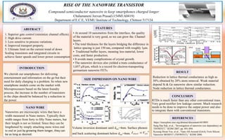
  • 1. RISE OF THE NANOWIRE TRANSISTOR Compound-semiconductor nanowire to keep smartphones charged longer Chalamaneni Jeevan Prasad (154M1A0419) Department of E.C.E, VEMU Institute of Technology, Chittoor 517124 ABSTRACT 1. Superior gate control (minimize channel effects). 2. High drive current. 3. Less sensitive to process variations. 4. Improved transport property. 5. Ultimate limit on the current trend of down Scaling transistors and integrated circuits to achieve faster speeds and lower power consumption INTRODUCTION NANO WIRE Nanowires are microscopic wires that have a width measured in Nano meters. Typically their width ranges from forty to fifty Nano meters, but their length is not so limited. Since they can be lengthened by simply attaching more wires end to end or just by growing them longer, they can be as long as desired. FEATURES SIZE IMPRESSION ON NANO WIRE REFERENCES CONCLUSION RESULT Reduction in lattice thermal conductance as high as 30% obtained by 20% atom removal. Weak material depend Si & Ge nanowire show similar reduction. Node reduction in lattice thermal conductance. RTDs is much faster than any other conventional trans. Very good rectifier low leakage current. Much research needs to be done to improve the output power and also to integrate them with conventional transistors. Volume inversion dominant until dnw=4nm. Surface phonon and back scattering dominant below dnw=4nm. We cherish our smartphones for delivering entertainment and information on the go but their need for daily charging is a problem. So when new smartphone models come on the market with Microprocessors based on the latest foundry process, the increase in the number of transistors in the chips should be balanced by a reduction in the power. https://ieeexplore.ieee.org/abstract/document/4419093  GSDSAT VI  Sung Dae Suk, et al., “Investigation of nanowire size dependency on TSNWFET,” IEDM 2007, pp. 891-894. Kyoung Hwan Yeo, et al., “Gate-All-Around (GAA) Twin Silicon Nanowire MOSFET (TSNWFET),” IEDM 2006. ▪ At around 10 nanometres from the interface, the quality of the material is very good, so we can grow the. Channel layers. ▪ The total thickness for the layers bridging the difference in lattice spacing is just 150 nm, compared with roughly 1μm. ▪ Traditional buffer layers, meaning less material, lower costs, and faster production. ▪ It avoids many complications of crystal growth. ▪ The nanowire devices also yielded a trans conductance of 1,057 μS/μm, which is a record for electron-transporting germanium nanowire FETs.