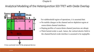
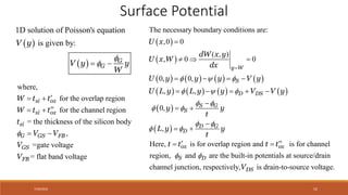
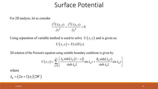
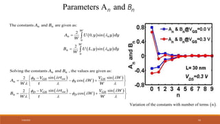
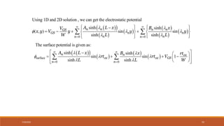
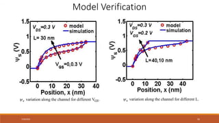
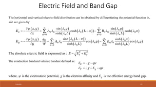
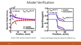
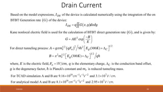
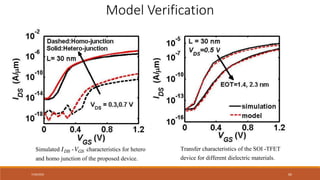
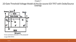
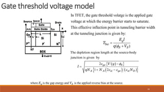
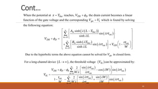
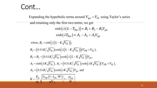
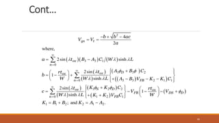
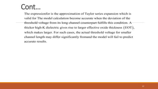
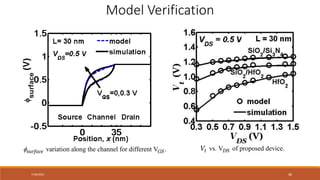
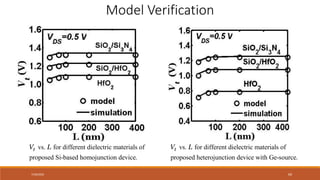
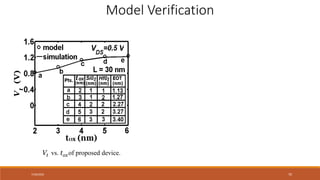
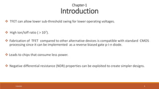
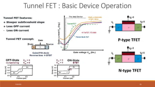
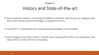
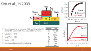
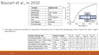
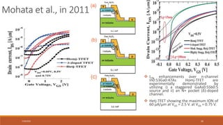
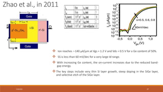
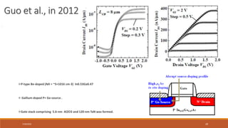
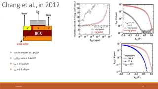
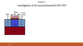
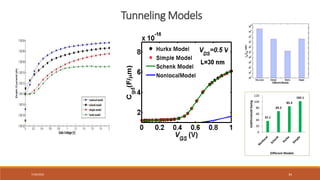
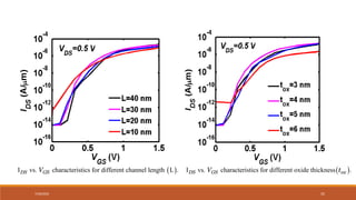
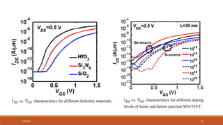
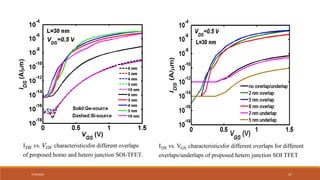
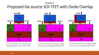
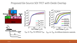
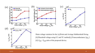
The document discusses a presentation given by Ashish Kumar Singh on his research investigating heterojunction silicon-on-insulator tunnel field effect transistors. The presentation outline includes an introduction discussing challenges with MOSFET scaling, the history and state-of-the-art of TFET research, the basic structure and operation of TFETs, investigations of Ge-source/Si strained SOI TFETs, a proposed Ge-source SOI TFET with oxide overlap, analytical modeling of the proposed device, conclusions and future work.

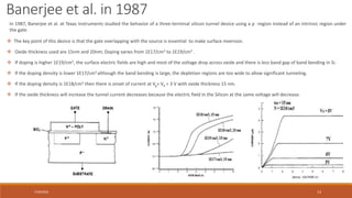
![References
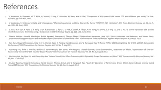
VDD(V)
Gate
Length
(µm)
ION
(µA/um)
IOFF
(pA/um)
ION/IOFF
SS@
(1nA/µm)
(mV/dec)
Steepest SS
(mV/dec)
EOT
(nm)
Body Structure
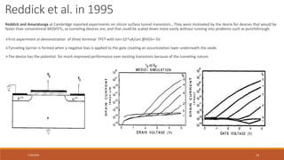
W.M. Reddick
et al.[5]
5 3µm 0.01 0.1 105 >600 >600 24 Bulk Si
P.F. Wang
et al. [17] 3 100 nm 0.02 10 2x10³ 450 375 6 Bulk Si
W.Y. Choi
et al. [18]
1 70nm 12.1 1000 1.2x10⁴ 60 52.8 2
SOI
TSi= 70 nm
F. Mayer
et.al [19]
1 0.02 1 2x10⁴ 330 42 3
(HFO2)
SOI
TSi = 20 nm
S.H. Kim
et al. [20] 0.5 0.25-5µm 0.42 0.14 3x10⁶ 80 40 3
SOI
TSi = 70 nm
(poly- Ge source)
K. Jeon
et al.[21] 1 20µm 1.2 0.017 7x10⁷ 70 46 0.9
(HFO2)
SOI
Tsi = 40 nm
(source Ni-Silicate + pocket formation)
R. Gandhi
et al.[22] 1.2 GAA 0.02
0.2
105 1000 50 4.5 Silicon NW diameter = 40 nm
(GAA structure)
Hsu-Yu Chang et al.[30]
1.1 100nm 1.4 0.1 1.4×10⁷ 77 46 3.5
(Al2O3)
SOI
TSi = 50nm
(with dopant pocket)
Our Work
0.5
30nm
33 8.55 3.4×10⁹ 44 37 1.4
(HfO2/SiO2)
SGOI
TSiGe = 20nm
(with germanium as source)
7/30/2022 47](https://image.slidesharecdn.com/sota-220730130705-bb5af5da/85/SOTA-pptx-47-320.jpg)