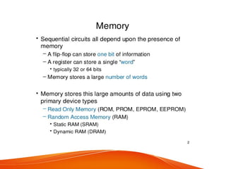
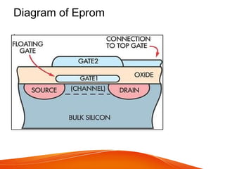
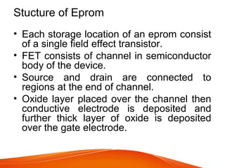
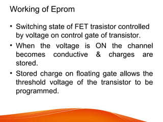
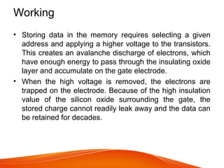
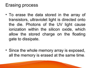
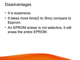
EPROM
Guide: Student name:
Prof:Priyanka Shridhar.Kullolli
Definition of EPROM
• EPROM is an acronym of Erasable programmable read-
only memory
• It is programmable read-only memory (programmable
ROM) that can be erased and re-used.
• Erasure is caused by shining an intense ultraviolet light
through a window that is designed into the memory chip.
• Although ordinary room light does not contain enough
ultraviolet light to cause erasure, bright sunlight can
cause erasure.
Comparision between ROM,PROM,EPROM
and EEPROM
• ROM is read only memory (in case you didn't know)
• PROM (programmable ROM)-can be programmed only
once. If there is a problem in the code on the chip then
this type of chip has to be thrown away since it is not
reprogrammable.
• EPROM-can be programmed and then erased (typically
erased with a UV eraser). These chips are easy to spot
because they have a "window" so they can be erased.
• EEPROM (electrically erasable and programmable)-
same as EPROM but is erased electrically. These don't
have a "window".
Diagram of Eprom
.
Stucture of Eprom
• Each storage location of an eprom consist
of a single field effect transistor.
• FET consists of channel in semiconductor
body of the device.
• Source and drain are connected to
regions at the end of channel.
• Oxide layer placed over the channel then
conductive electrode is deposited and
further thick layer of oxide is deposited
over the gate electrode.
Working of Eprom
• Switching state of FET trasistor controlled
by voltage on control gate of transistor.
• When the voltage is ON the channel
becomes conductive & charges are
stored.
• Stored charge on floating gate allows the
threshold voltage of the transistor to be
programmed.
Working
• Storing data in the memory requires selecting a given
address and applying a higher voltage to the transistors.
This creates an avalanche discharge of electrons, which
have enough energy to pass through the insulating oxide
layer and accumulate on the gate electrode.
• When the high voltage is removed, the electrons are
trapped on the electrode. Because of the high insulation
value of the silicon oxide surrounding the gate, the
stored charge cannot readily leak away and the data can
be retained for decades.
Erasing process
• To erase the data stored in the array of
transistors, ultraviolet light is directed onto
the die. Photons of the UV light cause
ionization within the silicon oxide, which
allow the stored charge on the floating
gate to dissipate.
• Since the whole memory array is exposed,
all the memory is erased at the same time.
Disadvantages
• It is expensive.
• It takes more time(2 to 3hrs) compare to
Eeprom.
• An EPROM eraser is not selective, it will
erase the entire EPROM.
• NO
Questions
Thank you

Eprom 3

  • 1.
  • 3.
    Definition of EPROM •EPROM is an acronym of Erasable programmable read- only memory • It is programmable read-only memory (programmable ROM) that can be erased and re-used. • Erasure is caused by shining an intense ultraviolet light through a window that is designed into the memory chip. • Although ordinary room light does not contain enough ultraviolet light to cause erasure, bright sunlight can cause erasure.
  • 4.
    Comparision between ROM,PROM,EPROM andEEPROM • ROM is read only memory (in case you didn't know) • PROM (programmable ROM)-can be programmed only once. If there is a problem in the code on the chip then this type of chip has to be thrown away since it is not reprogrammable. • EPROM-can be programmed and then erased (typically erased with a UV eraser). These chips are easy to spot because they have a "window" so they can be erased. • EEPROM (electrically erasable and programmable)- same as EPROM but is erased electrically. These don't have a "window".
  • 5.
  • 6.
    Stucture of Eprom •Each storage location of an eprom consist of a single field effect transistor. • FET consists of channel in semiconductor body of the device. • Source and drain are connected to regions at the end of channel. • Oxide layer placed over the channel then conductive electrode is deposited and further thick layer of oxide is deposited over the gate electrode.
  • 7.
    Working of Eprom •Switching state of FET trasistor controlled by voltage on control gate of transistor. • When the voltage is ON the channel becomes conductive & charges are stored. • Stored charge on floating gate allows the threshold voltage of the transistor to be programmed.
  • 8.
    Working • Storing datain the memory requires selecting a given address and applying a higher voltage to the transistors. This creates an avalanche discharge of electrons, which have enough energy to pass through the insulating oxide layer and accumulate on the gate electrode. • When the high voltage is removed, the electrons are trapped on the electrode. Because of the high insulation value of the silicon oxide surrounding the gate, the stored charge cannot readily leak away and the data can be retained for decades.
  • 9.
    Erasing process • Toerase the data stored in the array of transistors, ultraviolet light is directed onto the die. Photons of the UV light cause ionization within the silicon oxide, which allow the stored charge on the floating gate to dissipate. • Since the whole memory array is exposed, all the memory is erased at the same time.
  • 10.
    Disadvantages • It isexpensive. • It takes more time(2 to 3hrs) compare to Eeprom. • An EPROM eraser is not selective, it will erase the entire EPROM.
  • 11.