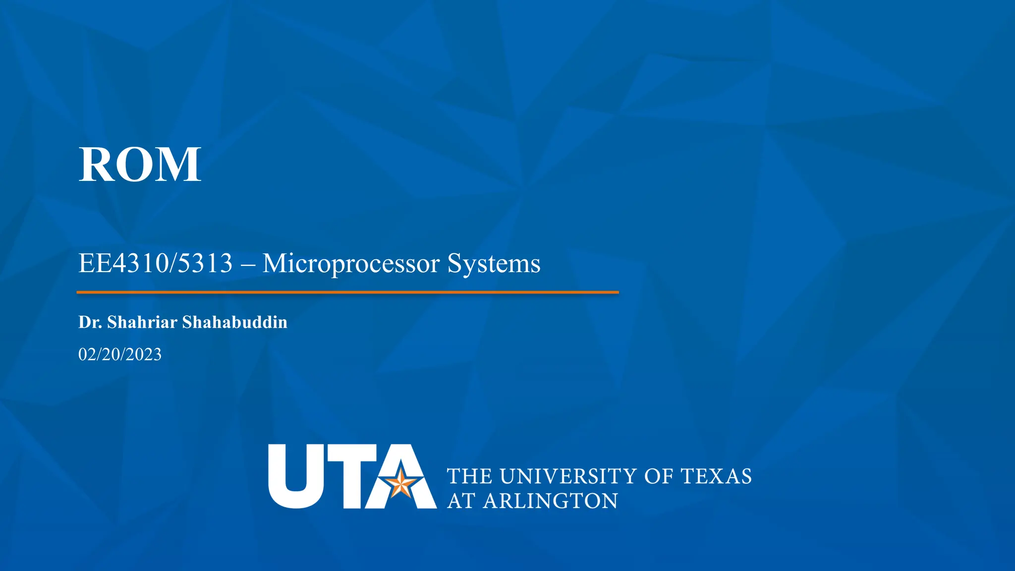
ROM Memory
ROMpermanently stores programs and data
Non-volatile memory
hold contents even if power supply is disconnected
3.
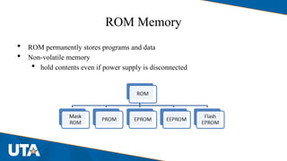
Mask ROM
ROMmeans read only memory
Mask ROM follows this definition
Hard wired
Cannot be changed electronically after manufacturing
Mask ROM is the oldest type of ROM
Mask ROM is factory programmed
Customer tells the manufacturer what the contents of the memory should be
Mask ROM has advantage in terms of cost
4.
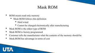
Programmable ROM (PROM)
Contents can be changed once after manufacture of the device
The data is then permanent and cannot be changed
In mask ROM data has to be written during manufacturing and in PROM data is
written after manufacturing
PROMs are used to store permanent data, e.g., firmware
PROM is programmed with a device called PROM programmer
This link shows you a PROM programmer:
https://www.advin.com/PROM-programmer.htm
5.
Erasable Programmable ROM(EPROM)
The main difference between EPROM and PROM is the data is erasable
EPROM can be reprogrammed
Data can be erased by exposure to strong ultraviolet light
EPROMs are easily recognizable by the transparent fused quartz window on the top
of the package
6.
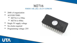
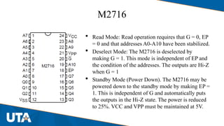
M2716
NMOS 16K (2Kx 8) UV EPROM
2048 x 8 organization
ACCESS TIME:
M2716-1 is 350ns
M2716 is 450ns
Single 5V supply voltage
No clocks required
Programming voltage: 25V
7.
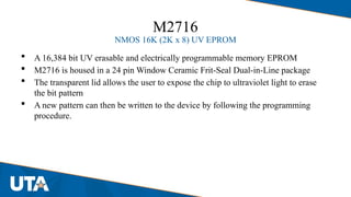
M2716
NMOS 16K (2Kx 8) UV EPROM
A 16,384 bit UV erasable and electrically programmable memory EPROM
M2716 is housed in a 24 pin Window Ceramic Frit-Seal Dual-in-Line package
The transparent lid allows the user to expose the chip to ultraviolet light to erase
the bit pattern
A new pattern can then be written to the device by following the programming
procedure.
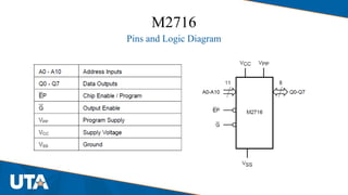
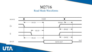
M2716
Read Mode:Read operation requires that G = 0, EP
= 0 and that addresses A0-A10 have been stabilized.
Deselect Mode: The M2716 is deselected by
making G = 1. This mode is independent of EP and
the condition of the addresses. The outputs are Hi-Z
when G = 1
Standby Mode (Power Down). The M2716 may be
powered down to the standby mode by making EP =
1. This is independent of G and automatically puts
the outputs in the Hi-Z state. The power is reduced
to 25%. VCC and VPP must be maintained at 5V.
M2716
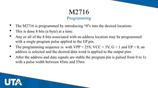
Programming
The M2716is programmed by introducing “0"s into the desired locations
This is done 8 bits (a byte) at a time.
Any or all of the 8 bits associated with an address location may be programmed
with a single program pulse applied to the EP pin.
The programming sequence is: with VPP = 25V, VCC = 5V, G = 1 and EP = 0, an
address is selected and the desired data word is applied to the output pins
After the address and data signals are stable the program pin is pulsed from 0 to 1s
with a pulse width between 45ms and 55ms
12.
M2716
Erasure Operation
TheM2716 is erased by exposure to high intensity ultraviolet light through the
transparent window.
The M2716 to be erased should be placed 1 inch away from the lamp and no filters
should be used.
It is recommended that the M2716 be kept out of direct sunlight.
The UV content of sunlight may cause a partial erasure of some bits in a relatively
short period of time.
Watch this:
https://www.youtube.com/watch?v=_sSuzDg4ntA&t=2s
13.
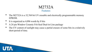
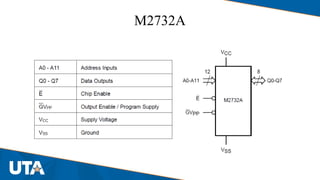
M2732A
Features
The M2732Ais a 32,768 bit UV erasable and electrically programmable memory
EPROM.
It is organized as 4,096 words by 8 bits
A 24 pin Window Ceramic Frit-Seal Dual-in-Line package
The UV content of sunlight may cause a partial erasure of some bits in a relatively
short period of time.
Electrically Erasable ProgrammableROM (EEPROM)
EEPROM stands for electrically erasable programmable read-only memory
Difference between EEPROM and EPROM
EEPROM can be erased with electric signals
The EEPROM does not need to be removed to be erased
Can be used with embedded systems
In microcontrollers, EEPROM stores relatively small amounts of data by allowing
individual bytes to be erased and reprogrammed
states of input or output devices so they it can be retained even if the
microcontroller loses power
17.
Flash Memory
Somecall flash a read-mostly memory (RMM)
Its also called
EAROM (electrically alterable ROM)
NOVRAM (nonvolatile RAM)
It has replaced the EPROM memory in most computer systems
Has its biggest impact in memory card for digital cameras and memory in MP3
audio players
18.
Flash Memory
Similarto the EEPROM technology
Flash memory can also read and write at the byte level, but can only erase data
at the block level
Flash memory has speed advantage over non-flash EEPROM
Flash memory costs much less than byte-programmable EEPROM and had become
the dominant memory type wherever a system required a significant amount of
non-volatile data
Flash memory as a replacement for hard drives: solid state drives
19.
Floating Gate MOSFET
Materialfor Flash Memory
The floating-gate transistor is a kind of transistor that is commonly used for
nonvolatile storage such as flash, EPROM and EEPROM memory.
Floating-gate transistors are almost always floating-gate MOSFETs.
Floating-gate MOSFETs are useful because of their ability to store an electrical
charge for extended periods of time even without a connection to a power supply
The charge stored on the floating gate can be modified by applying voltages to the
source, drain, body and control gate terminals such that the fields result in
phenomena like Fowler-Nordheim tunneling and hot carrier injection.
20.
Types of Flash
There are two types of Flash memory most commonly acknowledged: NAND and
NOR Flash
NOR Flash was the first of the two to be introduced in 1988 by Intel
NAND Flash was later introduced by Toshiba in 1989
Their main differences can be identified in their architecture
NOR and NAND are named for the way the floating gates of the memory cells
that hold data are interconnected in configurations that resemble a NOR or a
NAND logic gate
21.
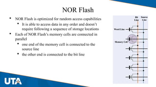
NOR Flash
NORFlash is optimized for random access capabilities
It is able to access data in any order and doesn’t
require following a sequence of storage locations
Each of NOR Flash’s memory cells are connected in
parallel
one end of the memory cell is connected to the
source line
the other end is connected to the bit line
22.
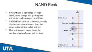
NAND Flash
NANDFlash is optimized for high-
density data storage and gives up the
ability for random access capabilities
NAND Flash cells are connected, usually
eight memory transistors at time, in a
series to the bit line called a string
This series connection reduces the
number of ground wires and bit lines
23.
NAND Flash
Datacan be read and programmed (written) in pages
but can only be erased at the level of entire blocks consisting of multiple pages
When a block is erased, all the cells are logically set to 1
Any cells that have been set to 0 by programming can only be reset to 1 by erasing
the entire block
This means that before new data can be programmed into a page that already
contains data, the current contents of the page plus the new data must be copied to
a new, erased page
24.
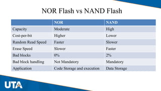
NOR Flash vsNAND Flash
NOR NAND
Capacity Moderate High
Cost-per-bit Higher Lower
Random Read Speed Faster Slower
Erase Speed Slower Faster
Bad blocks 0% 2%
Bad block handling Not Mandatory Mandatory
Application Code Storage and execution Data Storage
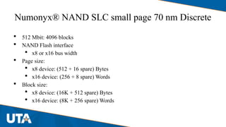
Numonyx® NAND SLCsmall page 70 nm Discrete
NAND structures where 16 cells are connected in series
The memory array is organized in blocks where each block contains 32 pages
The array is split into two areas
the main area
the spare area.
The main area of the array is used to store data
The spare area is typically used to store error correction codes, software flags or
bad block identification
30.
Numonyx® NAND SLCsmall page 70 nm Discrete
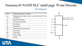
Chip enable (E): If CE is not asserted, the NAND device will remain in standby
mode and not respond to any control signals
Write enable (W): W is responsible for clocking data, address, or commands into
the NAND
Read enable (R): R will enable the output data buffers
Command latch enable (CL): When CLE is high, commands are latched into the
NAND command register on the rising edge of the WE# signal.
Address latch enable (AL): When ALE is high, addresses are latched into the
NAND address register on the rising edge of the WE# signal.
Ready/busy (RB): If the NAND device is busy, the R/B# signal will be asserted low
Editor's Notes
#1 - Exam 1: Mark Breedwell
- Made a mistake in the maths
#3 Mask ROM is a read-only memory whose contents are programmed by the integrated circuit manufacturer (rather than by the user). The customer tells the manufacturer what the content of the memory should be, lets say we go to Samsung
The main advantage of mask ROM is its cost. Per bit, mask ROM is more compact than any other kind of semiconductor memory. Since the cost of an integrated circuit strongly depends on its size, mask ROM is significantly cheaper than any other kind of semiconductor memory.
However, the one-time masking cost is high and there is a long turn-around time from design to product phase. Design errors are costly: if an error in the data or code is found, the mask ROM is useless and must be replaced in order to change the code or data.
#4 PROMs are manufactured blank and, depending on the technology, can be programmed at wafer, final test, or in system
A polyfuse is a one-time-programmable memory component used in semiconductor circuits for storing unique data like chip identification numbers or memory repair data, but more usually small to medium volume production of read only memory devices or microcontroller chips.
#5 quartz window
- can be expensive
Became OTP
OTP EPROM (whether separate or part of a larger chip) is being increasingly replaced by EEPROM for small sizes, where the cell cost isn't too important, and flash for larger sizes.
#7 Glass frit bonding, also referred to as glass soldering or seal glass bonding, describes a wafer bonding technique with an intermediate glass layer.
#18 Because erase cycles are slow, the large block sizes used in flash memory erasing give it a significant speed advantage over non-flash EEPROM
Flash memory costs much less than byte-programmable EEPROM and had become the dominant memory type wherever a system required a significant amount of non-volatile data
The Flash Memory is also called Flash ROM. In microcontrollers, the Flash stores the application code to be run. After we write an application, like blind LEDs for example, the application is compiled, the binary files are produced and they are stored in the flash of a microcontroller.
Flash can also have the bootloader. It loads the operating system within the computer memory when a computer is started or booted up. Take an example of the mobile.
#21 - The NOR Flash architecture provides enough address lines to map the entire memory range.
- This gives the advantage of random access and short read times, which makes it ideal for code execution.
- Another advantage is 100% known good bits for the life of the part.
- Disadvantages include larger cell size resulting in a higher cost per bit and slower write and erase speeds
#22 NAND-based Flash memory is ideal for high capacity data storage, while NOR-based Flash memory is best suited for code storage and execution, generally in small capacities
https://www.embedded.com/flash-101-nand-flash-vs-nor-flash/
#23 If a suitable erased page is available, the data can be written to it immediately
If no erased page is available, a block must be erased before copying the data to a page in that block
#24 NAND-based Flash memory is ideal for high capacity data storage, while NOR-based Flash memory is best suited for code storage and execution, generally in small capacities
https://www.embedded.com/flash-101-nand-flash-vs-nor-flash/
#25 https://flashdba.com/2014/06/20/understanding-flash-blocks-pages-and-program-erases/
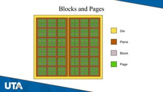
The package is the memory chip, i.e. the black rectangle with little electrical connectors sticking out of it.
Each package contains one or more dies (for example one, two, or four). The die is the smallest unit that can independently execute commands or report status.
Each die contains one or more planes (usually one or two). Identical, concurrent operations can take place on each plane, although with some restrictions.
Each plane contains a number of blocks, which are the smallest unit that can be erased. Remember that, it’s really important.
Each block contains a number of pages, which are the smallest unit that can be programmed (i.e. written to).
Read: Page
Write: Page
Erase: Block
Flash differs from EEPROM in that erasures are done in blocks, rather than individual bits. Because erasing is a relatively slow operation, and must be done before writing, performing the erase in a large block makes large write operations faster, by virtue of erasing a large number of bits in parallel.
Erasing in blocks also allows simplifications to the IC, reducing cost. Economies of scale further reduce cost of flash over EEPROM, as flash is used in great quantities these days for solid-state drives, while EEPROM is used in much smaller quantities.
It's by definition. A flash memory that allows writing individual bits is called EEPROM.
https://en.wikipedia.org/wiki/EEPROM
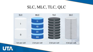
#26 SLCs are the fastest type of SSD. They’re also more durable and less error-prone
TLC 500MB - 1GB
QLC NAND can pack a whole lot more data than other types, but, right now, QLC drives take a big hit on drive performance. This is especially true when the cache runs out during large file transfers (40 GB or higher). This might be a short-term problem, as manufacturers try to optimize QLCs.
#27 Discrete means a discrete memory chip, separate or standalone memory chip