Electronics Basic Concepts
•
5 likes•1,498 views

The document provides an overview of basic electronics engineering concepts including: 1. The evolution of electronics from early experiments with vacuum tubes in the 1850s to the invention of the transistor in 1947 and integrated circuits in 1958. 2. Atomic structure including Bohr's atomic model, quantum numbers, and the periodic table which orders elements by atomic number and electron configuration. 3. How electrons behave in solids, forming energy bands, and the types of bonding that occur between atoms in solids including metallic, covalent and ionic bonding.

Recommended
More Related Content
What's hot
What's hot (20)
Similar to Electronics Basic Concepts
Similar to Electronics Basic Concepts (20)
More from A B Shinde
More from A B Shinde (20)
Recently uploaded
Recently uploaded (20)
Electronics Basic Concepts
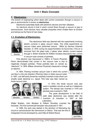
- 1. Basic Electronics Engineering (Basic Concepts) Prepared By Mr. A. B. Shinde, Electronics Engg., PVPIT, Budhgaon 1 Geissler William Crookes Shockley Bardeen Brattain Jack Kilby Unit- I: Basic Concepts 1. Electronics: The branch of engineering which deals with current conduction through a vacuum or gas or semiconductor is known as electronics. Electronics essentially deals with electronic devices and their utilisation. An electronic device is that in which current flows through a vacuum or gas or semiconductor. Such devices have valuable properties which enable them to function and behave as the friend of man today. 1.1. Evolution of Electronics: The electronics field was dawned with the experiments involving electric currents in glass vacuum tubes. The initial experiments on vacuum tubes were performed around 1850s by German Scientist Geissler. In 1878, during his experimentation he found that, if the air is removed from the glass tube, it glows when electric current passes through it. British Scientist Sir William Crookes discovered that, current in vacuum tube consists of particles. First electron was discovered in 1890‟s. A French Physicist, Perrin demonstrated that current in the vacuum tube is due to negatively charged particles. These particles later on named as, “electrons”. In 1909, Milikan (American Physicist) measured a charge on electron. In 1904, Fleming invented vacuum tube in which the current can flow in only one direction (Fleming Valve or diode vacuum tube). In 1907, Lee deForest (American scientist) invented a tube which can amplify weak electrical a.c. signal. This tube was later named as triode vacuum tube. In 1915, this triode vacuum tube was used in oscillator circuits as well as in telephone system. The tetrode was invented in 1916 and pentode was invented in 1926. The great development in the field of solid state electronics was started after the invention of transistor in 1947 at Bell Laboratory. Walter Brattain, John Bardeen & William Shockley invented the transistor. The first commercial transistor was produced in 1951. In 1958, the work was started in the direction of fabricating the circuit on semiconductor like Germanium or Silicon. That was the first IC (Integrated Circuit) developed by Jack Kilby & Robert Noyce.
- 2. Basic Electronics Engineering (Basic Concepts) Prepared By Mr. A. B. Shinde, Electronics Engg., PVPIT, Budhgaon 2 Structure of an Atom 2. Atomic Structure: The most fundamental unit of solid is atom. Structure of an atom mainly consists of three particles: electrons, protons and neutrons. Electron has negative charge equal to 1.6 × 10⁻¹⁹ coulombs. A Neutron has no charge. Protons and Neutrons are located inside the nucleus. 2.1. Bohr’s Atomic Model: In 1913, Neils Bohr, (Danish Physicist) gave clear explanation of atomic structure. According to Bohr: (i) An atom consists of a positively charged nucleus around which negatively charged electrons revolve in different circular orbits. (ii) The electrons can revolve around the nucleus only in certain permitted orbits i.e. orbits of certain radii are allowed. (iii) The electrons in each permitted orbit have a certain fixed amount of energy. The larger the orbit (i.e. larger radius), the greater is the energy of electrons. (iv) If an electron is given additional energy (e.g. heat, light etc.), it is lifted to the higher orbit. Figure shows the structure of silicon atom. It has 14 electrons. Two electrons revolve in the first orbit, 8 in the second orbit and 4 in the third orbit. The first, second, third orbits etc. are also known as K, L, M orbits respectively. These electrons can revolve only in permitted orbits and not in any arbitrary orbit. Thus, all radii between r1 and r2 or between r2 and r3 are forbidden.
- 3. Basic Electronics Engineering (Basic Concepts) Prepared By Mr. A. B. Shinde, Electronics Engg., PVPIT, Budhgaon 3 2.2. Permitted Orbits: We know that the electron revolves around the nucleus in fixed orbits, called energy level or shells. These orbits are represented by the letters K, L, M, N, … etc. counted from nucleus onwards. Thus the K-shell is closest to the nucleus. The next is L-shell and so on. Sometimes the K, L, M, N, are also designated as 1, 2, 3, 4, etc. The maximum number of electrons in any shell are given by the relation 2n2 where n is an integer, called as principal quantum number. Thus, for K-shell, n = 1. i. e. can have maximum 2(1)2 = 2 electrons. Similarly, L-shell with n= 2, can have 2(2)2 = 8 electrons. M-shell with n= 3, can have 2(3)2 = 18 electrons and N-shell with n= 4, can have 2(4)2 = 32 electrons. The distribution of electrons in an atom is subject to the following two rules: 1. The outer most shell of an atom cannot accommodate more than 8 electrons, even if it has the capacity to accommodate more electrons, 2. The shell of an atom just prior to the outer most shell, cannot accommodate more than 8 electrons. 2.3. Quantum Numbers: According to Bohr‟s postulates, there is only one orbit corresponding to each value of the principal quantum number n. However, it is being proved that all orbits (except n = 1 orbit) consist of more than one orbit called sub-orbits. This group of sub-orbits is collectively known as shell. For example, n = 1 shell or K-shell consists of only one orbit which may also be called its own sub-orbit or sub-shell. The n = 2 shell or L-shell consists of two sub-shells. Similarly, n = 3 shell or M-shell consists of three sub-shells. In other words, the number of sub-shells is equal to the n-value of the shell. The 2n2 electrons of the shell now get divided between these sub-shells. In order to distinguish between different sub-shells belonging to a given shell, a new quantum number called orbital (or azimuthal) quantum number l has been introduced. This quantum number can have integral values lying between zero and (n − 1) i.e. 0 ≤ l ≤ (n − 1). It is helpful in the following ways: (a) It gives the number of sub-shells which are contained in one shell. The number of sub-shells is equal to the number of values which l can have subject to the restriction 0 ≤ l ≤ (n − 1) as shown in figure. (b) It helps to distinguish between different sub-shells of a shell by its different values for each sub-shell. Consider the following cases : 1. n = 1 shell. Here, l = 0. Hence, K-shell has only one sub shell with two quantum numbers of n = 1 and l = 0.
- 4. Basic Electronics Engineering (Basic Concepts) Prepared By Mr. A. B. Shinde, Electronics Engg., PVPIT, Budhgaon 4 2. n = 2 shell. Here, l = 0, 1. Hence, this shell has two sub-shells which are distinguishable from each other by their different quantum numbers of n = 2, l = 0 and n = 2, l = 1. 3. n = 3 shell. Here l = 0, 1, 2, showing that M-shell has three sub-shells which differ in their l-values. The two quantum numbers for the three sub-shells are: n = 3, l = 0; n = 3, l = 1; n = 3, l = 2. Orbit No. of orbits Total no. of electrons No. of sub orbits Max. electrons in sub orbit K n = 1 2 1s 2 L n = 2 8 2s, 2p 2, 6 M n = 3 18 3s, 3p, 3d 2, 6, 10 N n = 4 32 4s, 4p, 4d, 4f 2, 6, 10, 14 Quantum Numbers are numbers that describe the quantum mechanical properties of orbits: 1. The Principal Quantum Number (n) 2. The Secondary Quantum Number (l) 3. The Magnetic Quantum Number (ml) 4. The Spin Quantum Number (ms ) 2.3.1. The Principal Quantum Number (n) • Gives the main energy level or shell • Describes the size and energy of an atomic orbital • n can have any integer value greater than zero n = 1, 2, 3, 4, … 2.3.2. The Secondary Quantum Number (l) • Gives the sub level or sub shell • Describes the shape of the orbital: • Sometimes called the „Angular Momentum Quantum Number‟ • L can have any integer values from 0 to n-1
- 5. Basic Electronics Engineering (Basic Concepts) Prepared By Mr. A. B. Shinde, Electronics Engg., PVPIT, Budhgaon 5 o e.g. n l 1 0 2 0,1 3 0,1,2 4 0,1,2,3 • The energy of the orbital depends on lonely in a multi-electron case; for electrons with the same n, energy of l=1 < l=2 < l=3… 2.3.3. Magnetic Quantum Number (ml) It determines the spatial orientation of elliptical electron orbits with respect to an applied magnetic field. There are restrictions on the orientations of the electron orbits because of which they are said to be space quantized. Whereas l determines the orbital angular momentum, ml represents the magnitude of the component of angular momentum along the direction of the magnetic field. Looked from a different angle, ml determines the number of sub-sub shells in a given shell. This quantum number can have any one of the (2l + 1) values ranging from + l to − l including zero i.e. l, (l − 1), (l − 2).........2, 1, 0, − 1, − 2,.......... − (l − 2), − (l − 1), − l. Each sub-subshell can accommodate a maximum of 2 electrons, so that maximum number of electrons in a shell becomes 2(2l + 1). 2.3.4. Magnetic Spin Quantum Number (ms) It has been found that an electron spins around its own mechanical axis as it rotates in orbit around the nucleus. When the electron is subjected to a magnetic field, its spin axis orientates itself either parallel to or antiparallel to the direction of the field. This quantum number arises out of quantization of the electron spin angular momentum. It determines the spin orientation up or down and has correspondingly two values of + 1/2 and − 1/2. 3. Periodic table: The periodic table is a tabular arrangement of the chemical elements, ordered by their atomic number (number of protons), electron configurations, and recurring chemical properties. This ordering shows periodic trends, such as elements with similar behaviour in the same column. Within one row (period) the elements are metals on the left side and non-metals on the right side. The rows of the table are called periods; the columns are called groups. The Russian chemist Dmitri Mendeleev published the first widely recognized periodic table in 1869. Mendeleev's periodic table has been expanded and refined with the discovery or synthesis of further new elements and the development of new theoretical models to explain chemical behaviour.
- 6. Basic Electronics Engineering (Basic Concepts) Prepared By Mr. A. B. Shinde, Electronics Engg., PVPIT, Budhgaon 6 All elements from atomic numbers 1 (hydrogen) to 118 (oganesson) have been discovered or synthesized, with the most recent additions being confirmed by the International Union of Pure and Applied Chemistry (IUPAC) in 2015 and officially named in 2016. Each chemical element has a unique atomic number (Z) representing the number of protons in its nucleus. Most elements have differing numbers of neutrons among different atoms, with these variants being referred to as isotopes. For example, carbon has three naturally occurring isotopes: all of its atoms have six protons and most have six neutrons as well, but about one percent has seven neutrons, and a very small fraction have eight neutrons. Isotopes are never separated in the periodic table; they are always grouped together under a single element. Groups A group or family is a vertical column in the periodic table. Groups usually have more significant periodic trends than periods and blocks. Elements in the same group tend to have a shared chemistry and exhibit a clear trend in properties with increasing atomic number. However, in some parts of the periodic table, such as the d- block and the f-block, horizontal similarities can be as important as, or more pronounced than, vertical similarities. Periods A period is a horizontal row in the periodic table. Although groups generally have more significant periodic trends, there are regions where horizontal trends are more significant than vertical group trends, such as the f-block, where the lanthanides and actinides form two substantial horizontal series of elements.
- 7. Basic Electronics Engineering (Basic Concepts) Prepared By Mr. A. B. Shinde, Electronics Engg., PVPIT, Budhgaon 7 Blocks Specific regions of the periodic table can be referred to as blocks in recognition of the sequence in which the electron shells of the elements are filled. Each block is named according to the subshell in which the "last" electron notionally resides. The s- block comprises the first two groups (alkali metals and alkaline earth metals) as well as hydrogen and helium. The p-block comprises the last six groups, which are groups 13 to 18 in IUPAC group numbering and contains, among other elements, all of the metalloids. The d-block comprises groups 3 to 12 and contains all of the transition metals. The f-block, often offset below the rest of the periodic table, has no group numbers and comprises lanthanides and actinides. Metals, metalloids and nonmetals According to their shared physical and chemical properties, the elements can be classified into the major categories of metals, metalloids and nonmetals. Metals are generally shiny, highly conducting solids that form alloys with one another and salt-like ionic compounds with nonmetals (other than the noble gases). The majority of nonmetals are coloured or colourless insulating gases; nonmetals that form compounds with other nonmetals feature covalent bonding. In between metals and nonmetals are metalloids, which have intermediate or mixed properties. 4. Electrons in solids (Energy Bands in Solids) It is found that each of the energy levels of an atom splits into N levels of energy where N is the number of atoms in the crystal. Each original energy level becomes a band of very closely-spaced levels of slightly different energy. Consider the case of Na crystal which consists of an ordered array of many closely- packed sodium atoms usually referred to as crystal lattice. Each Na atom has 11 electrons arranged in different shells and sub-shells. For a small sodium crystal containing 1020 atoms, the band formed by splitting of s-sub shell has 2 electronic levels (one with spin up and the others with spin down). Similarly in a p-band there will be 6 × 10²⁰ closely packed levels because there are 6 electrons in a filled p subshell. In general, in an assembly of N atoms, the number of possible energy states is N. Since only two electrons of opposite spin can occupy the same state (as per Pauli‟s Exclusion Principle discussed earlier), the maximum number of electrons which these N states can occupy is 2N. 5. Bonding in solids: What are solids? The collection of closely packed atoms resulting in the formation of bulk materials called solids. Solids are one among the three fundamental states of matter. In solids, the atoms are tightly packed together and have a definite shape and structure that can´t be retained or changed.
- 8. Basic Electronics Engineering (Basic Concepts) Prepared By Mr. A. B. Shinde, Electronics Engg., PVPIT, Budhgaon 8 Solids are mainly classified into TWO types. Crystalline Solids Amorphous Solids What is bonding in solids? The binding force that exists due to charge distribution in the atoms of the elements is known as Bonding. Different charge distributions lead to different types of bonding. The rigidity of a solid arises from the fact that the atoms in the solid are held together by Inter-atomic forces, called interatomic bonds. The spatial arrangement of atoms, in a solids, is strongly influenced by the nature of these bonds, which in turn is influenced by the electronic structure of the atoms. The interatomic bonds, in solids, have the following two important Characteristics: 1. Bond energy: The energy corresponding to the position of the atoms, at which the bonds are formed, is called bond energy. The bonds, which possess higher bond energy, are called stronger bonds and those which possess smaller bond energy are called weaker bonds. 2. Bond length: It may be defined as centre-to-centre distance of the bonding atoms. The stronger bonds have smaller bond length, while weaker bonds have larger bond length. As mentioned above, the bond energy is used to classify the various types of bonds in two broad categories i.e. stronger or primary bonds and weak or secondary bonds. There are mainly two types of bonds: Primary bonds: Ionic bond, covalent bonds & metallic bonds Secondary bonds: dipole forces, induction forces, Van der Waal‟s forces & hydrogen bonds 5.1. Primary Bonds: 5.1.1. Ionic Bonds The bond formed between two oppositely charged ions, which are produced by the transfer of electrons from one atom to another, is called ionic bond or electrovalent bond. Atom, which loses the electron, acquires a positive charge and becomes a positive ion. On the other hand, an atom which gains the electron acquires a negative charge and becomes a negative ion. Hence, both ions becomes oppositely charges ions. The electrostatic force of attraction between oppositely charged ions forms ionic bond. It has been found that; ionic bond is readily formed between the atoms of alkali metals and halogen atoms. The formation of ionic bond in case of sodium chloride is illustrated below:
- 9. Basic Electronics Engineering (Basic Concepts) Prepared By Mr. A. B. Shinde, Electronics Engg., PVPIT, Budhgaon 9 Atomic Numbers of: Na = 11 (2, 8, 1) Cl = 17 (2, 8, 7) 5.1.2. Covalent Bonds The bond which is formed by sharing of electrons between two atoms is called as covalent bond. The sharing of electrons takes place in such a way that each atom, gets the stable electron arrangement. We know that, atomic number of silicon is 14 and distribution of electrons is 2, 8, 4 i.e. last orbit has 4 valence electrons and it needs 4 more electrons to complete the last orbit to become stable. It gets these 4 electrons by sharing 4 electrons, each from neighbouring silicon atoms as shown in figure. 5.1.3. Metallic Bonds In all metals, it has been observed that, the electrons in the outer most shell are loosely held by their nucleus. Due this, the electrons in the outer most shell requires very less energy to detach themselves from nucleus. At room temperature, all metal atoms lose their outer most shell electrons which form an electrons cloud or common pool of electrons. These electrons are free to move anywhere within the crystal. After loosing the electrons, the atom becomes positive ion. Hence, metals can be considered as array of positive ions surrounded by large number of free electrons. The electrostatic force of attraction between electron cloud and positive ions forms a bond, which is called as metallic bond.
- 10. Basic Electronics Engineering (Basic Concepts) Prepared By Mr. A. B. Shinde, Electronics Engg., PVPIT, Budhgaon 10 5.2. Secondary Bonds Secondary bonds are bonds where there is no sharing or transfer of electrons. In primary bonding forces are short range strong forces, but the secondary bonding forces are long range weak forces. As compared to primary bonds, secondary bonds are weaker in nature. These bonds are due to atomic or molecular dipoles, both permanent and temporary. The following types of secondary bonding occurs in organic compounds: Dipole forces Induction forces van der Waal‟s forces Hydrogen bonding 5.2.1. Dipole forces: When two atoms having difference in electronegativity are bonded together, the resulting bond is not neutral but bears partial negative and positive charges or polarity. Such polar bonds are said to have dipole. The greater the difference of electronegativity; the greater the intensity of charges and greater will be the dipole. 5.2.3. Induction forces: When a molecule having a dipole comes near a non polar molecule, the later experiences slight charge separation due to interaction with polar molecule. The forces acting due to such induced charge are called induction forces. Induction forces are weak and temporary forces and they die as and when the permanent dipole moves away.
- 11. Basic Electronics Engineering (Basic Concepts) Prepared By Mr. A. B. Shinde, Electronics Engg., PVPIT, Budhgaon 11 5.2.3. Van der Waal’s forces: In any material all the molecule attract one another since the nucleus of each molecule exert slight attraction on electrons of the other molecules, so that the molecule come nearer to one another. However, the repulsion between the electrons of different molecules becomes prominent if they come too close to one other and thus keeps them at a certain distance. The forces acting to keep the molecules together are called van der Waal‟s forces. Due to van der Waal‟s forces the free movement of molecules in a substance is affected. Thus stronger the forces, the more restricted the movement. Van der Waal's forces are of two types. The first type is as a result of electrostatic attraction between two permanent dipoles. Permanent dipoles are formed in asymmetric molecules where there are permanent positive and negative regions due to difference in electronegativities of the constituent elements. The second type of Van der Waal's bond is formed due to temporary dipoles. A temporary dipole is formed in a symmetric molecule but which has fluctuations of charges giving rise to partial dipole moments for only a few moments. 5.2.4. Hydrogen bonds: Hydrogen bonds are relatively stronger than Van der Waal's forces but compared to primary bonds they are weak. When hydrogen bonded to a molecule comes in vicinity of another atom having a lone pair, like oxygen, on another molecule, it forms secondary bond with it. For example the hydrogen of a water molecule forms secondary bond with oxygen of the other water molecule. Hydrogen bonds are of two types- intermolecular and intramolecular. In intermolecular hydrogen bonds, the bonds are between hydrogen atom of one molecule and electronegative atom of another e. g. o-nitrophenol. In intramolecular hydrogen bonds, the bonds are between hydrogen atom and electronegative atom of the same molecule but such that they do not have any covalent interactions e. g. p-nitrophenol.
- 12. Basic Electronics Engineering (Basic Concepts) Prepared By Mr. A. B. Shinde, Electronics Engg., PVPIT, Budhgaon 12 6. Atom arrangement in materials: Matter exists in any of the three states namely, solids, liquids and gasses. In the gaseous state, the atoms or molecules are separated from each other by large distance. Gases are characterized by their ability to fill the shape of their container completely, no matter the volume. This is because the atoms in gases move at incredibly high speeds in random directions. This randomness spreads the gas particles out very far from each other, expanding the gas to fill the volume of the container it's in. In liquids, the atoms or molecules are closer to each other as compared to gasses. Liquids fill the shape of their container, but they don't change volume. Their molecules move quickly, but not quite at the speed that gases do. Since they're slower, they stay closer together and collide more frequently. This keeps them within the original volume. In solids, atoms are closest to each other as compared to any other material state. The atoms in solids barely move at all; it's more of a vibration. Therefore, solids aren't very mobile, comparatively. They don't fill up the shape of their container at all. Solids hold their form, since the atoms aren't going very far from their original points. 7. Crystalline structure of metals: Metals are about two thirds of all the elements and about 24% of the mass of the planet. They are all around us in such forms as steel structures, copper wires, aluminium foil and gold jewellery. The properties of metals are: strength, ductility, high melting point, thermal and electrical conductivity and toughness. The strength of metals is that, the atoms are held together by strong bonds. Structure of metals is defined as the arrangement of atoms within the metal. In all metals and some non-metals, the atoms are arranged in systematic and well ordered manner. Such structures are known as crystalline structures. Solids whose atoms are not arranged in systematic pattern are called as non-crystalline or amorphous solids e. g. rubber & glass etc. In the crystalline structure, the atoms are arranged in three-dimensional periodic fashion. The periodic arrangement of atoms in a crystal is called lattice. The thermal vibrations associated with the atom are centred about this position. There are several different types of crystal lattice depending upon the symmetry and internal structure. One of them is the cubic crystal lattice. There are three basic types of cubic crystal lattice. These are simple cubic (SC), base centred cubic (BCC) and face centred cubic (FCC).
- 13. Basic Electronics Engineering (Basic Concepts) Prepared By Mr. A. B. Shinde, Electronics Engg., PVPIT, Budhgaon 13 7.1. Simple Cubic: Figure (a) shows a SC crystal. In this cell, each corner of the cubic lattice is occupied by an atom that has six equidistant nearest neighbouring atoms. The dimension “a” is called the lattice constant. Only podium is crystallised into the simple cubic lattice. 7.2. Base Centred Cubic: Figure (b) shows a BCC cell. In this cell, each atom has eight nearest neighbouring atoms. Crystals exhibiting the BCC lattices include those of sodium and tungsten. 7.3. Face Centred Cubic: Figure (c) shows a FCC cell. This cell has one atom at each of the six cubic faces in addition to the eight corner atoms. In an FCC lattice, each atom has 12 nearest neighbouring atoms. A large number of elements exhibit the FCC lattice form. These include aluminium, copper, gold and platinum. 8. Classification of engineering materials: The materials coming under the material science are broadly categorised into: Metals and alloys, Ceramics, Organic polymers, Composite materials 8.1. Metals and Alloys: Metals have polycrystalline structure. Normally major metals are in solid states at normal temperature. In general, metals have good electrical and thermal conductivity. Pure metals have very low mechanical strength, which sometimes does not match with requirement for certain application. To overcome this draw back alloys are used. Alloys are the composition of two or more metals or metal and non-metals together. Metals and alloys have relatively high strength, high stiffness, ductility or formability, and shock resistance. 8.2. Ceramic Materials: They are non-metallic solids. Beach sand and rocks are examples of naturally occurring ceramics. Ceramics are made of inorganic compounds such as Oxides, Nitrides and Carbides. Ceramics are as soft as clay or as hard as stone and concrete. Usually, they
- 14. Basic Electronics Engineering (Basic Concepts) Prepared By Mr. A. B. Shinde, Electronics Engg., PVPIT, Budhgaon 14 are crystalline in form. Ceramic materials possess exceptional Structural, Electrical, Magnetic, Chemical and Thermal properties. These ceramic materials are now extensively used in different engineering fields. Examples: Silica, glass, cement, concrete, garnet, MgO, Cds, ZnO, SiC etc. 8.3. Organic Polymers: Polymers are typically organic materials. Polymers are chemical compounds made up of a large number of identical components linked together like chains. Polymers are the raw materials used to make what are commonly called plastics and rubber. Polymers typically are good electrical and thermal insulators. Although they have lower strength, polymers have a very good strength-to-weight ratio. Polymers are used in many applications, including electronic devices. Example: Plastics, PVC, Synthetic Rubbers etc. 8.4. Composite Material: The main idea in developing composite material is to blend the properties of different materials. Composite material consists of more than one material type. These are formed from two or more materials, producing properties not found in any single material. Fiber glass, a combination of glass and a polymer, is an example. Concrete and plywood are other familiar composites. Many new combinations include ceramic fibers in metal or polymer matrix. Concrete, plywood, and fiberglass are examples of composite materials. STRUCTURE PROPERTIES Metals/ Alloys Any metallic element /alloy Simple crystalline structure Metallic atomic bonding High conductivity Not transparent to visible light Strong, Ductile Ceramics Compounds of metals and non-metals Primarily ionic atomic bonding Ceramics are crystalline Glasses are amorphous, glass-ceramics are devitrified glasses Insulative Refractory Wear resistant Strong Hard Chemically stable High melting temps Polymers Organic compounds Large molecular structures in a chain or network configuration Atomic bonding is covalent on the chains 5-95% crystalline Very ductile (elastic and plastic) Low density Low strength Low melting temp High chemical reactivity Composites Engineered materials of more than one type, usually a matrix material with fibers. Could be anything, depending on constituents, relative amounts and geometry
- 15. Basic Electronics Engineering (Basic Concepts) Prepared By Mr. A. B. Shinde, Electronics Engg., PVPIT, Budhgaon 15 9. Classification of solids: All the solids are classified broadly in below mentioned categories: Conductors, Semiconductors, Dielectric materials, Magnetic materials, 9.1. Conductors: Conductors (e.g. copper, aluminium) are those substances which easily allow the passage of electric current through them. It is because there are a large number of free electrons available in a conductor. In terms of energy band, the valence and conduction bands overlap each other. Due to this overlapping, a slight potential difference across a conductor causes the free electrons to constitute electric current. 9.2. Semiconductors: Semiconductors (e.g. germanium, silicon etc.) are those substances whose electrical conductivity lies in between conductors and insulators. In terms of energy band, the valence band is almost filled and conduction band is almost empty. Further, the energy gap between valence and conduction bands is very small. Therefore, comparatively smaller electric field (smaller than insulators but much greater than conductors) is required to push the electrons from the valence band to the conduction band. 9.3. Dielectric material: A dielectric material is a substance that is a poor conductor of electricity, but an efficient supporter of electrostatic fields. Dielectric material is an electrical insulator that can be polarized by an applied electric field. If the flow of current between opposite electric charge poles is kept to a minimum while the electrostatic lines of flux are not interrupted, an electrostatic field can store energy. This property is useful in capacitors, especially at radio frequencies. Most dielectric materials are solid. Examples include porcelain (ceramic), mica, glass, plastics, and the oxides of various metals. Some liquids and gases can serve as good dielectric materials. Dry air is an excellent dielectric, and is used in variable capacitors. The lower the dielectric loss (the proportion of energy lost as heat), the more effective is a dielectric material. 9.4. Magnetic material: Magnetic materials are utilized in the creation and distribution of electricity. They are used for the storage of data on audiotape and videotape and on computer disks. In the world of medicine, they are used in body scanners and in a range of applications where they are attached to or implanted into the body. The home entertainment market relies on magnetic materials in applications such as PCs, CD players, televisions, games consoles and loudspeakers. Magnetic materials are classified in terms of their magnetic properties and their uses. If a material is easily magnetized and demagnetized then it is referred to as a soft
- 16. Basic Electronics Engineering (Basic Concepts) Prepared By Mr. A. B. Shinde, Electronics Engg., PVPIT, Budhgaon 16 magnetic material, whereas if it is difficult to demagnetize then it is referred to as a hard (or permanent) magnetic material. 9.4.1. Diamagnetic materials: Diamagnetic materials are slightly repelled by a magnetic field and the material does not retain the magnetic properties when the external field is removed. They have a weak, negative susceptibility to magnetic fields. In diamagnetic materials all the electron are paired so there is no permanent net magnetic moment per atom. Diamagnetic properties arise from the realignment of the electron paths under the influence of an external magnetic field. Most elements in the periodic table, including copper, silver and gold are diamagnetic. 9.4.2. Paramagnetic materials: These materials are slightly attracted by a magnetic field and the material does not retain the magnetic properties when the external field is removed. They have a small, positive susceptibility to magnetic fields. Paramagnetic properties are due to the presence of some unpaired electrons, and from the realignment of the electron paths caused by the external magnetic field. Paramagnetic materials include magnesium, molybdenum, lithium, and tantalum. 9.4.3. Ferromagnetic materials: They exhibit a strong attraction to magnetic fields and are able to retain their magnetic properties after the external field has been removed. They have a large, positive susceptibility to an external magnetic field. Ferromagnetic materials have some unpaired electrons so their atoms have a net magnetic moment. When a ferromagnetic material is in the unmagnitized state, the domains are nearly randomly organized and the net magnetic field for the part as a whole is zero. When a magnetizing force is applied, the domains become aligned to produce a strong magnetic field within the part. Iron, nickel, and cobalt are examples of ferromagnetic materials. 10. Energy band description of materials: Important Energy Bands in Solids: As discussed before, individual K, L, M etc. energy levels of an isolated atom are converted into corresponding bands when the atom is in a solid state. Though there are a number of energy bands in solids, the following are of particular importance: 10.1. Valence band: The range of energies (i.e. band) possessed by valence electrons is known as valence band. The electrons in the outermost orbit of an atom are known as valence electrons. In a normal atom, valence band has the electrons of highest energy. This band may be completely or partially filled. For instance, in case of inert gases, the valence band is full whereas for other materials, it is only partially filled. The partially filled band can accommodate more electrons.
- 17. Basic Electronics Engineering (Basic Concepts) Prepared By Mr. A. B. Shinde, Electronics Engg., PVPIT, Budhgaon 17 10.2. Conduction band: In certain materials (e.g. metals), the valence electrons are loosely attached to the nucleus. Even at room temperature, some of the valence electrons may get detached to become free electrons. These free electrons are responsible for the conduction of current in a conductor. The range of energies (i.e. band) possessed by conduction band electrons is known as conduction band. All electrons in the conduction band are free electrons. If a substance has empty conduction band, it means current conduction is not possible in that substance. Generally, insulators have empty conduction band. On the other hand, it is partially filled for conductors. 10.3. Forbidden energy gap: The separation between conduction band and valence band on the energy level diagram is known as forbidden energy gap. No electron of a solid can stay in a forbidden energy gap as there is no allowed energy state in this region. The width of the forbidden energy gap is a measure of the bondage of valence electrons to the atom. The greater the energy gap, more tightly the valence electrons are bound to the nucleus. In order to push an electron from valence band to the conduction band (i.e. to make the valence electron free), external energy equal to the forbidden energy gap must be supplied.