Single Stage IC Amplifier
Mr. A. B. Shinde
A. B. Shinde
Contents…
 IC Design philosophy,
 Comparison of MOSFET and BJT,
 IC Biasing: Current sources,
 IC Biasing: Current mirrors and
 IC Biasing: Current steering circuits,
 High frequency response
2
A. B. Shinde
3
IC Design Philosophy
A. B. Shinde
IC Design Philosophy
• Constraints and opportunities & features of the IC design philosophy:
• Resistors:
• To minimize the chip area, large and even moderate-size resistors are to
be avoided.
• Transistors can be made small and cheaply, and the use of transistors in
preference to resistors is appreciated.
• As a result, the classical biasing arrangement, is abandoned in IC
amplifiers, rather constant-current sources are implemented with
transistors operating in the active mode for biasing.
• The collector and drain resistors in amplifiers are replaced with constant-
current sources that have much higher incremental resistance.
4
A. B. Shinde
IC Design Philosophy
• Constraints and opportunities & features of the IC design philosophy:
• Capacitors:
• Chip-area considerations make it impossible to fabricate large-valued
capacitors such as those employed for signal coupling and bypass in
discrete-circuit amplifiers.
• Therefore, IC amplifiers are all direct coupled.
• Small-size capacitors, in the picofarad and fraction-of-a-picofarad range,
are easy to fabricate in IC MOS technology.
• Such capacitors can be combined with MOS amplifiers and MOS
switches to realize a wide variety of analog and digital signal-processing
functions.
5
A. B. Shinde
IC Design Philosophy
• Constraints and opportunities & features of the IC design philosophy:
• Power Supplies:
• CMOS process technologies are capable of producing devices with a
12-nm channel length.
• To avoid breaking down the thin oxide layers (less than 1 nm) used in
these devices, power supplies are limited to 1 V.
• Low power-supply voltages keeps the power dissipation within
acceptable limits.
• However, the use of such low dc power-supply voltages presents the
circuit designer with a lost of challenges. For instance, MOS transistors
must be operated with overdrive voltages of only 0.1 V to 0.2 V.
6
A. B. Shinde
IC Design Philosophy
• Constraints and opportunities & features of the IC design philosophy:
• Device Variety:
• The designer of discrete circuits, has limit to use the transistors.
• But, the IC designer has the freedom to specify the device dimensions
and to utilize device matching and arrays of devices having dimensions
with specified ratios.
• For instance, one can utilize an array of bipolar transistors whose
emitter–base–junction areas have binary-weighted ratios.
• CMOS technology provides even more flexibility, with the W and L
values of MOS transistors selected to fit a very wide range of design
requirements.
7
A. B. Shinde
IC Design Philosophy
• Constraints and opportunities & features of the IC design philosophy:
• Bipolar Technology:
• BJTs are still used in special analog applications, such as high-quality
general-purpose op-amp packages.
• Bipolar circuits can also be combined with CMOS circuits in innovative
and exciting ways in what is known as BiCMOS technology.
8
A. B. Shinde
IC Design Philosophy
• Constraints and opportunities & features of the IC design philosophy:
• CMOS Technology:
• Currently majority of analog integrated circuits are designed using
CMOS technology.
• This was initially motivated by the need to be compatible with digital
circuits.
• Now, the richness and the versatility that CMOS provides the analog
designers has even stronger reason for its dominance.
9
A. B. Shinde
10
MOSFET Vs BJT
A. B. Shinde
MOSFET Vs BJT
11
Parameter MOSFET BJT
Types n Channel, p Channel npn, pnp
Output Current is controlled by the input gate
voltage.
is controlled by the input base
current.
ESD Risk Easily damaged by ESD
Electrostatic Discharge.
ESD is rarely a problem
A. B. Shinde
MOSFET Vs BJT
12
Parameter MOSFET BJT
Gain Very high current gain which is
nearly constant for varying drain
currents.
Lower current gain and it is not
constant. It decreases when the
collector current increases.
Gain increases as temperature
increases.
Input
Resistance
Very high.
For AC signals, much lower due
to the capacitance of the device.
Low
Input Current Picoamps (approximately zero). Microamps or Milliamps
Saturation VDS = 20 mV
Even lower heat dissipation
when saturated.
VCE = 200 mV
Low heat dissipation when
saturated.
Switching
Speed
Faster than Bipolar Slower than MOSFETs.
Frequency
Response
Better frequency response Inferior frequency response
A. B. Shinde
MOSFET Vs BJT
13
Parameter MOSFET BJT
Voltages When fully turned on, the
potential drop across the device
(VDS) is about 20 mV.
When fully turned on, the
potential drop across the device
(VCE) is about 200 mV.
Bias (input)
Voltages
N Channel MOSFETS need +2
to +4 volts to turn them on.
Base current starts to flow with an
input voltage of about +0.7V
Thermal
Runaway
When MOSFETS heat up, the
current flowing through them
decreases.
They are less likely to be
destroyed by overheating.
When bipolar transistors heat up,
the gain increases and so the
current through them increases
too.
This can cause thermal runaway.
Cost More Expensive Lower Cost
A. B. Shinde
MOSFET Vs BJT
14
A. B. Shinde
MOSFET Vs BJT
15
A. B. Shinde
MOSFET Vs BJT
16
A. B. Shinde
MOSFET Vs BJT
17
A. B. Shinde
MOSFET Vs BJT
18
A. B. Shinde
MOSFET Vs BJT
19
A. B. Shinde
20
IC Biasing
A. B. Shinde
IC Biasing
• On an IC chip with a number of amplifier stages, a constant dc current is
generated at one location and is then replicated at various other
locations for biasing the various amplifier stages through a process
known as current steering.
• This approach has the advantage that the effort expended on generating
a predictable and stable reference current, usually utilizing a precision
resistor external to the chip or a special circuit on the chip, need not be
repeated for every amplifier stage.
• Furthermore, the bias currents of the various stages track each other in
case of changes in power-supply voltage or in temperature.
21
A. B. Shinde
22
IC Biasing:
Current Source Circuit
A. B. Shinde
Current Source
• Figure shows the circuit of a simple
MOSFET constant-current source.
• For transistor Q1, the drain is shorted to
its gate, forcing it to operate in the
saturation mode with
23
Basic MOSFET
constant current source
The drain current of Q1 is supplied by
VDD through resistor R, which in most
cases would be outside the IC chip.
Since the gate currents are zero,
A. B. Shinde
Current Source
• Consider Q2: It has the same VGS as Q1;
thus, if we assume that it is operating in
saturation, its drain current, which is the
output current IO of the current source,
will be
24
Basic MOSFET
constant current source
Relation between the output current IO to
the reference current IREF as follows:
A. B. Shinde
Current Source
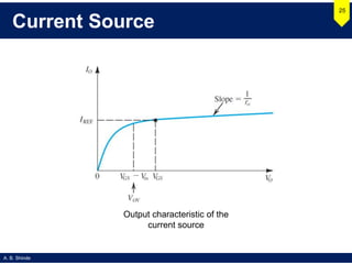
25
Output characteristic of the
current source
A. B. Shinde
26
IC Biasing:
Current Mirror Circuit
A. B. Shinde
Current Mirror
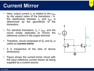
• Here, output current IO is related to the IREF
by the aspect ratios of the transistors i. e.
the relationship between IO and IREF is
determined by the geometries of the
transistors.
• For identical transistors, IO = IREF, and the
circuit simply replicates or mirrors the
reference current in the output terminal.
• Therefore, circuit composed of Q1 and Q2 is
called as current mirror
• It is irrespective of the ratio of device
dimensions.
• Figure shows the current-mirror circuit with
the input reference current shown as being
supplied by a current source.
27
A. B. Shinde
Current Mirror
• Effect of VO on IO:
• In constant current source circuit, we assumed Q2 is operating in
saturation mode; so as to supply a constant-current output.
• To ensure that Q2 is saturated, the circuit to which the drain of Q2 is to
be connected must establish a drain voltage VO that satisfies the
relationship
VO ≥ VGS −Vtn
or, in terms of the overdrive voltage VOV of Q1 and Q2,
VO ≥ VOV
The current source will operate properly with VO as low as VOV, which is
a few tenths of a volt.
28
A. B. Shinde
Current Mirror
• Consider, identical devices Q1 and Q2.
• The drain current of Q2, IO, will equal the current in Q1, IREF, at the value
of VO that causes the two devices to have the same VDS, that is, at
VO = VGS.
As VO is increased above this value, IO will increase according to the
incremental output resistance ro2 of Q2.
• In summary, the current source circuit and the current mirror circuit have
a finite output resistance Ro
29
where IO is output current and VA2 is the Early voltage of Q2which is
proportional to the transistor channel length.
A. B. Shinde
Current Mirror
• Example: Given VDD = 3V and
using IREF =100 μA, design the
circuit shown in figure to obtain an
output current whose nominal
value is 100 μA. Find R if Q1 and
Q2 are matched and have channel
lengths of 1 μm, channel widths of
10 μm, Vt = 0.7 V, and kn = 200
μA/V2. What is the lowest possible
value of VO? Assuming that for this
process technology, the Early
voltage VA =20 V/μm, find the
output resistance of the current
source. Also, find the change in
output current resulting from a
+1 V change in VO.
30
A. B. Shinde
Current Mirror
• Solution:
31
For the transistors used, L = 1 μm. Thus
Therefore
and
A. B. Shinde
Current Mirror
The output current will be 100 μA at VO = VGS = 1 V.
If VO changes by +1 V, the corresponding change in IO will be
32
A. B. Shinde
33
IC Biasing:
Current Steering Circuit
A. B. Shinde
Current Steering Circuit
• Constant current source once generated can be replicated to provide dc
bias or load currents for the various amplifier stages in an IC.
• This process is known as current steering.
• Current mirrors can also be used to implement these current-steering
function.
34
A. B. Shinde
Current Steering Circuit
• Here Q1 together with R determine the reference current IREF. Transistors
Q1, Q2, and Q3 form a two-output current mirror,
35
current-steering circuit.
A. B. Shinde
Current Steering Circuit
• To ensure operation in the saturation region, the voltages at the drains of
Q2 and Q3 are constrained as follows:
VD2,VD3 ≥ −VSS +VGS1 −Vtn
or, equivalently,
VD2,VD3 ≥ −VSS +VOV1
where VOV1 is the overdrive voltage at which Q1, Q2, and Q3 are
operating. In other words, the drains of Q2 and Q3 will have to remain
higher than −VSS by at least the overdrive voltage, which is usually a few
tenths of a volt.
• Here, current I3 is fed to the input side of a current mirror formed by
PMOS transistors Q4 and Q5.
• This mirror provides
36
where I4 = I3
A. B. Shinde
Current Steering Circuit
• To keep Q5 in saturation, its drain voltage should be
VD5 ≤ VDD −|VOV5 |
where VOV5 is the overdrive voltage at which Q5 is operating.
37
A. B. Shinde
38
High Frequency Response
A. B. Shinde
High Frequency Response
• The amplifier circuits do not employ bypass capacitors.
• The various stages in an integrated-circuit cascade amplifier are directly
coupled; that is, they do not utilize large coupling capacitors.
39
The frequency response of these direct-coupled or d c amplifiers takes the
general form shown in figure, where gain remains constant at midband
value AM down to zero frequency (dc).
The gain, however, falls off at the high-frequency end due to the internal
capacitances of the transistor.
A. B. Shinde
High Frequency Response
• High-Frequency Gain Function
• The amplifier gain, taking into account the internal transistor
capacitances, can be expressed as a function of the complex-frequency
variables in the general form
A(s) = AM FH (s)
where AM is the midband gain.
• The value of AM can be determined by analyzing the amplifier equivalent
circuit while neglecting the effect of the transistor internal
capacitances—that is, by assuming that they act as perfect open
circuits.
• By taking these capacitances into account, the gain acquires the factor
FH(s), which can be expressed in terms of its poles and zeros, which are
usually real, as follows:
40
A. B. Shinde
High Frequency Response
• Determining the 3-dB Frequency fH:
• In amplifier high-frequency band that is close to the midband is more
important because the designer needs to estimate – and if needed
modify the value of the upper 3-dB frequency fH (or ωH; fH = ωH/2π).
• In many cases the zeros are either at infinity or such high frequencies as
to be of little significance to the determination of ωH.
• If in addition one of the poles, say ωP1, is of much lower frequency than
any of the other poles, then this pole will have the greatest effect on the
value of the amplifier ωH.
• In other words, this pole will dominate the high-frequency response of
the amplifier, and the amplifier is said to have a dominant-pole response.
• In such cases the function FH(s) can b e approximated by
41
which is the transfer function of a first-order low-pass network.
A. B. Shinde
High Frequency Response
• Determining the 3-dB Frequency fH:
• A dominant pole exists if the lowest-frequency pole is at least two
octaves (a factor of 4) away from the nearest pole or zero.
• If a dominant pole does not exist, the 3-dB frequency ωH can be
determined from a plot of |FH (jω)|.
• An approximate formula for ωH can be derived as follows:
Consider, for simplicity, the case of a circuit having two poles and two
zeros in the high-frequency band; that is,
42
Substituting s = j ω and taking the squared magnitude gives
A. B. Shinde
High Frequency Response
43
Since ωH is usually smaller than the frequencies of all the poles and
zeros, we may neglect the terms containing ω4
H and solve for ωH to
obtain
Determining the 3-dB Frequency fH:
A. B. Shinde
High Frequency Response
• Determining the 3-dB Frequency fH:
• This relationship can be extended to any number of poles and zeros as
44
A. B. Shinde
Unit-III: Single Stage IC amplifiers
• CS and CF amplifiers with loads,
• High frequency response of CS and CF amplifiers,
• CG and CB amplifiers with active loads,
• High frequency response of CG and CB amplifiers,
• Cascade amplifiers.
• CS and CE amplifiers with source (emitter) degeneration source and
emitter followers,
• Some useful transfer parings,
• Current mirrors with improved performance.
• SPICE examples.
45
This presentation is published only for educational purpose
abshinde.eln@gmail.com

MOSFETs: Single Stage IC Amplifier

  • 1.
    Single Stage ICAmplifier Mr. A. B. Shinde
  • 2.
    A. B. Shinde Contents… IC Design philosophy,  Comparison of MOSFET and BJT,  IC Biasing: Current sources,  IC Biasing: Current mirrors and  IC Biasing: Current steering circuits,  High frequency response 2
  • 3.
    A. B. Shinde 3 ICDesign Philosophy
  • 4.
    A. B. Shinde ICDesign Philosophy • Constraints and opportunities & features of the IC design philosophy: • Resistors: • To minimize the chip area, large and even moderate-size resistors are to be avoided. • Transistors can be made small and cheaply, and the use of transistors in preference to resistors is appreciated. • As a result, the classical biasing arrangement, is abandoned in IC amplifiers, rather constant-current sources are implemented with transistors operating in the active mode for biasing. • The collector and drain resistors in amplifiers are replaced with constant- current sources that have much higher incremental resistance. 4
  • 5.
    A. B. Shinde ICDesign Philosophy • Constraints and opportunities & features of the IC design philosophy: • Capacitors: • Chip-area considerations make it impossible to fabricate large-valued capacitors such as those employed for signal coupling and bypass in discrete-circuit amplifiers. • Therefore, IC amplifiers are all direct coupled. • Small-size capacitors, in the picofarad and fraction-of-a-picofarad range, are easy to fabricate in IC MOS technology. • Such capacitors can be combined with MOS amplifiers and MOS switches to realize a wide variety of analog and digital signal-processing functions. 5
  • 6.
    A. B. Shinde ICDesign Philosophy • Constraints and opportunities & features of the IC design philosophy: • Power Supplies: • CMOS process technologies are capable of producing devices with a 12-nm channel length. • To avoid breaking down the thin oxide layers (less than 1 nm) used in these devices, power supplies are limited to 1 V. • Low power-supply voltages keeps the power dissipation within acceptable limits. • However, the use of such low dc power-supply voltages presents the circuit designer with a lost of challenges. For instance, MOS transistors must be operated with overdrive voltages of only 0.1 V to 0.2 V. 6
  • 7.
    A. B. Shinde ICDesign Philosophy • Constraints and opportunities & features of the IC design philosophy: • Device Variety: • The designer of discrete circuits, has limit to use the transistors. • But, the IC designer has the freedom to specify the device dimensions and to utilize device matching and arrays of devices having dimensions with specified ratios. • For instance, one can utilize an array of bipolar transistors whose emitter–base–junction areas have binary-weighted ratios. • CMOS technology provides even more flexibility, with the W and L values of MOS transistors selected to fit a very wide range of design requirements. 7
  • 8.
    A. B. Shinde ICDesign Philosophy • Constraints and opportunities & features of the IC design philosophy: • Bipolar Technology: • BJTs are still used in special analog applications, such as high-quality general-purpose op-amp packages. • Bipolar circuits can also be combined with CMOS circuits in innovative and exciting ways in what is known as BiCMOS technology. 8
  • 9.
    A. B. Shinde ICDesign Philosophy • Constraints and opportunities & features of the IC design philosophy: • CMOS Technology: • Currently majority of analog integrated circuits are designed using CMOS technology. • This was initially motivated by the need to be compatible with digital circuits. • Now, the richness and the versatility that CMOS provides the analog designers has even stronger reason for its dominance. 9
  • 10.
  • 11.
    A. B. Shinde MOSFETVs BJT 11 Parameter MOSFET BJT Types n Channel, p Channel npn, pnp Output Current is controlled by the input gate voltage. is controlled by the input base current. ESD Risk Easily damaged by ESD Electrostatic Discharge. ESD is rarely a problem
  • 12.
    A. B. Shinde MOSFETVs BJT 12 Parameter MOSFET BJT Gain Very high current gain which is nearly constant for varying drain currents. Lower current gain and it is not constant. It decreases when the collector current increases. Gain increases as temperature increases. Input Resistance Very high. For AC signals, much lower due to the capacitance of the device. Low Input Current Picoamps (approximately zero). Microamps or Milliamps Saturation VDS = 20 mV Even lower heat dissipation when saturated. VCE = 200 mV Low heat dissipation when saturated. Switching Speed Faster than Bipolar Slower than MOSFETs. Frequency Response Better frequency response Inferior frequency response
  • 13.
    A. B. Shinde MOSFETVs BJT 13 Parameter MOSFET BJT Voltages When fully turned on, the potential drop across the device (VDS) is about 20 mV. When fully turned on, the potential drop across the device (VCE) is about 200 mV. Bias (input) Voltages N Channel MOSFETS need +2 to +4 volts to turn them on. Base current starts to flow with an input voltage of about +0.7V Thermal Runaway When MOSFETS heat up, the current flowing through them decreases. They are less likely to be destroyed by overheating. When bipolar transistors heat up, the gain increases and so the current through them increases too. This can cause thermal runaway. Cost More Expensive Lower Cost
  • 14.
  • 15.
  • 16.
  • 17.
  • 18.
  • 19.
  • 20.
  • 21.
    A. B. Shinde ICBiasing • On an IC chip with a number of amplifier stages, a constant dc current is generated at one location and is then replicated at various other locations for biasing the various amplifier stages through a process known as current steering. • This approach has the advantage that the effort expended on generating a predictable and stable reference current, usually utilizing a precision resistor external to the chip or a special circuit on the chip, need not be repeated for every amplifier stage. • Furthermore, the bias currents of the various stages track each other in case of changes in power-supply voltage or in temperature. 21
  • 22.
    A. B. Shinde 22 ICBiasing: Current Source Circuit
  • 23.
    A. B. Shinde CurrentSource • Figure shows the circuit of a simple MOSFET constant-current source. • For transistor Q1, the drain is shorted to its gate, forcing it to operate in the saturation mode with 23 Basic MOSFET constant current source The drain current of Q1 is supplied by VDD through resistor R, which in most cases would be outside the IC chip. Since the gate currents are zero,
  • 24.
    A. B. Shinde CurrentSource • Consider Q2: It has the same VGS as Q1; thus, if we assume that it is operating in saturation, its drain current, which is the output current IO of the current source, will be 24 Basic MOSFET constant current source Relation between the output current IO to the reference current IREF as follows:
  • 25.
    A. B. Shinde CurrentSource 25 Output characteristic of the current source
  • 26.
    A. B. Shinde 26 ICBiasing: Current Mirror Circuit
  • 27.
    A. B. Shinde CurrentMirror • Here, output current IO is related to the IREF by the aspect ratios of the transistors i. e. the relationship between IO and IREF is determined by the geometries of the transistors. • For identical transistors, IO = IREF, and the circuit simply replicates or mirrors the reference current in the output terminal. • Therefore, circuit composed of Q1 and Q2 is called as current mirror • It is irrespective of the ratio of device dimensions. • Figure shows the current-mirror circuit with the input reference current shown as being supplied by a current source. 27
  • 28.
    A. B. Shinde CurrentMirror • Effect of VO on IO: • In constant current source circuit, we assumed Q2 is operating in saturation mode; so as to supply a constant-current output. • To ensure that Q2 is saturated, the circuit to which the drain of Q2 is to be connected must establish a drain voltage VO that satisfies the relationship VO ≥ VGS −Vtn or, in terms of the overdrive voltage VOV of Q1 and Q2, VO ≥ VOV The current source will operate properly with VO as low as VOV, which is a few tenths of a volt. 28
  • 29.
    A. B. Shinde CurrentMirror • Consider, identical devices Q1 and Q2. • The drain current of Q2, IO, will equal the current in Q1, IREF, at the value of VO that causes the two devices to have the same VDS, that is, at VO = VGS. As VO is increased above this value, IO will increase according to the incremental output resistance ro2 of Q2. • In summary, the current source circuit and the current mirror circuit have a finite output resistance Ro 29 where IO is output current and VA2 is the Early voltage of Q2which is proportional to the transistor channel length.
  • 30.
    A. B. Shinde CurrentMirror • Example: Given VDD = 3V and using IREF =100 μA, design the circuit shown in figure to obtain an output current whose nominal value is 100 μA. Find R if Q1 and Q2 are matched and have channel lengths of 1 μm, channel widths of 10 μm, Vt = 0.7 V, and kn = 200 μA/V2. What is the lowest possible value of VO? Assuming that for this process technology, the Early voltage VA =20 V/μm, find the output resistance of the current source. Also, find the change in output current resulting from a +1 V change in VO. 30
  • 31.
    A. B. Shinde CurrentMirror • Solution: 31 For the transistors used, L = 1 μm. Thus Therefore and
  • 32.
    A. B. Shinde CurrentMirror The output current will be 100 μA at VO = VGS = 1 V. If VO changes by +1 V, the corresponding change in IO will be 32
  • 33.
    A. B. Shinde 33 ICBiasing: Current Steering Circuit
  • 34.
    A. B. Shinde CurrentSteering Circuit • Constant current source once generated can be replicated to provide dc bias or load currents for the various amplifier stages in an IC. • This process is known as current steering. • Current mirrors can also be used to implement these current-steering function. 34
  • 35.
    A. B. Shinde CurrentSteering Circuit • Here Q1 together with R determine the reference current IREF. Transistors Q1, Q2, and Q3 form a two-output current mirror, 35 current-steering circuit.
  • 36.
    A. B. Shinde CurrentSteering Circuit • To ensure operation in the saturation region, the voltages at the drains of Q2 and Q3 are constrained as follows: VD2,VD3 ≥ −VSS +VGS1 −Vtn or, equivalently, VD2,VD3 ≥ −VSS +VOV1 where VOV1 is the overdrive voltage at which Q1, Q2, and Q3 are operating. In other words, the drains of Q2 and Q3 will have to remain higher than −VSS by at least the overdrive voltage, which is usually a few tenths of a volt. • Here, current I3 is fed to the input side of a current mirror formed by PMOS transistors Q4 and Q5. • This mirror provides 36 where I4 = I3
  • 37.
    A. B. Shinde CurrentSteering Circuit • To keep Q5 in saturation, its drain voltage should be VD5 ≤ VDD −|VOV5 | where VOV5 is the overdrive voltage at which Q5 is operating. 37
  • 38.
    A. B. Shinde 38 HighFrequency Response
  • 39.
    A. B. Shinde HighFrequency Response • The amplifier circuits do not employ bypass capacitors. • The various stages in an integrated-circuit cascade amplifier are directly coupled; that is, they do not utilize large coupling capacitors. 39 The frequency response of these direct-coupled or d c amplifiers takes the general form shown in figure, where gain remains constant at midband value AM down to zero frequency (dc). The gain, however, falls off at the high-frequency end due to the internal capacitances of the transistor.
  • 40.
    A. B. Shinde HighFrequency Response • High-Frequency Gain Function • The amplifier gain, taking into account the internal transistor capacitances, can be expressed as a function of the complex-frequency variables in the general form A(s) = AM FH (s) where AM is the midband gain. • The value of AM can be determined by analyzing the amplifier equivalent circuit while neglecting the effect of the transistor internal capacitances—that is, by assuming that they act as perfect open circuits. • By taking these capacitances into account, the gain acquires the factor FH(s), which can be expressed in terms of its poles and zeros, which are usually real, as follows: 40
  • 41.
    A. B. Shinde HighFrequency Response • Determining the 3-dB Frequency fH: • In amplifier high-frequency band that is close to the midband is more important because the designer needs to estimate – and if needed modify the value of the upper 3-dB frequency fH (or ωH; fH = ωH/2π). • In many cases the zeros are either at infinity or such high frequencies as to be of little significance to the determination of ωH. • If in addition one of the poles, say ωP1, is of much lower frequency than any of the other poles, then this pole will have the greatest effect on the value of the amplifier ωH. • In other words, this pole will dominate the high-frequency response of the amplifier, and the amplifier is said to have a dominant-pole response. • In such cases the function FH(s) can b e approximated by 41 which is the transfer function of a first-order low-pass network.
  • 42.
    A. B. Shinde HighFrequency Response • Determining the 3-dB Frequency fH: • A dominant pole exists if the lowest-frequency pole is at least two octaves (a factor of 4) away from the nearest pole or zero. • If a dominant pole does not exist, the 3-dB frequency ωH can be determined from a plot of |FH (jω)|. • An approximate formula for ωH can be derived as follows: Consider, for simplicity, the case of a circuit having two poles and two zeros in the high-frequency band; that is, 42 Substituting s = j ω and taking the squared magnitude gives
  • 43.
    A. B. Shinde HighFrequency Response 43 Since ωH is usually smaller than the frequencies of all the poles and zeros, we may neglect the terms containing ω4 H and solve for ωH to obtain Determining the 3-dB Frequency fH:
  • 44.
    A. B. Shinde HighFrequency Response • Determining the 3-dB Frequency fH: • This relationship can be extended to any number of poles and zeros as 44
  • 45.
    A. B. Shinde Unit-III:Single Stage IC amplifiers • CS and CF amplifiers with loads, • High frequency response of CS and CF amplifiers, • CG and CB amplifiers with active loads, • High frequency response of CG and CB amplifiers, • Cascade amplifiers. • CS and CE amplifiers with source (emitter) degeneration source and emitter followers, • Some useful transfer parings, • Current mirrors with improved performance. • SPICE examples. 45
  • 46.
    This presentation ispublished only for educational purpose abshinde.eln@gmail.com