Dual Active Bridge Converter a Bidirectional Isolated DC DC Converter
The document presents a comprehensive M.Tech research project on the modeling and control of a Dual Active Bridge (DAB) converter, focusing on its objectives, mathematical modeling, modes of operation, and testing methodologies. It covers aspects such as zero voltage switching, power flow equations, and various modulation techniques, alongside hardware implementation and testing results. The project concludes that the DAB converter is effective for bidirectional power flow applications and outlines further references for in-depth understanding.
Dual Active Bridge Converter a Bidirectional Isolated DC DC Converter
1.
Modelling and Controlof Dual Active Bridge
(DAB) Converter
M.Tech. Research Project
Presented by
Ritwik Saini
(Roll No.: 222EE3436)
Under the supervision of
Dr. Susovon Samanta
Department of Electrical Engineering
National Institute of Technology, Rourkela
December, 2023
2.
Contents:-
• Objective
• Introduction
•Modes of operation of DAB converter
• Mathematical Modeling of DAB Converter
• Power derivation
• Zero Voltage Switching
• Design Parameters of DAB
• Hardware testing
a. Gate driver testing
b. Open loop testing of DAB
• Small signal analysis
• Close loop control
• Reference
3.
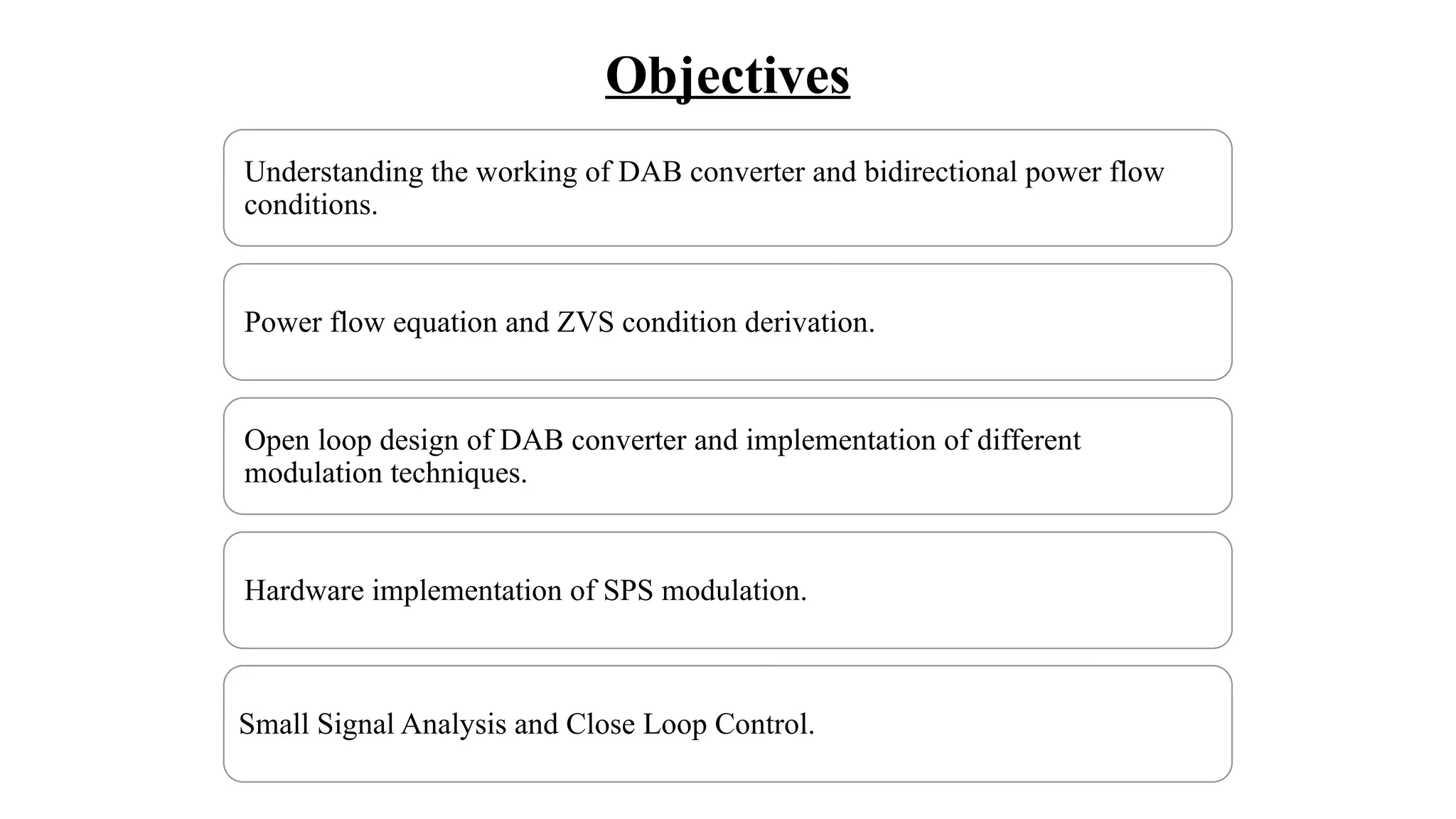
Objectives
Understanding the workingof DAB converter and bidirectional power flow
conditions.
Power flow equation and ZVS condition derivation.
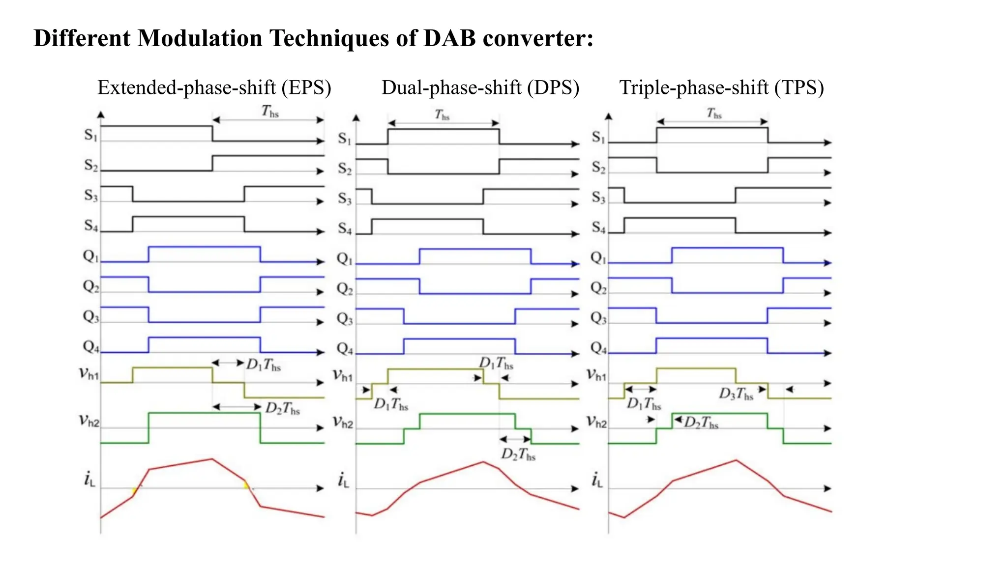
Open loop design of DAB converter and implementation of different
modulation techniques.
Hardware implementation of SPS modulation.
Small Signal Analysis and Close Loop Control.
4.
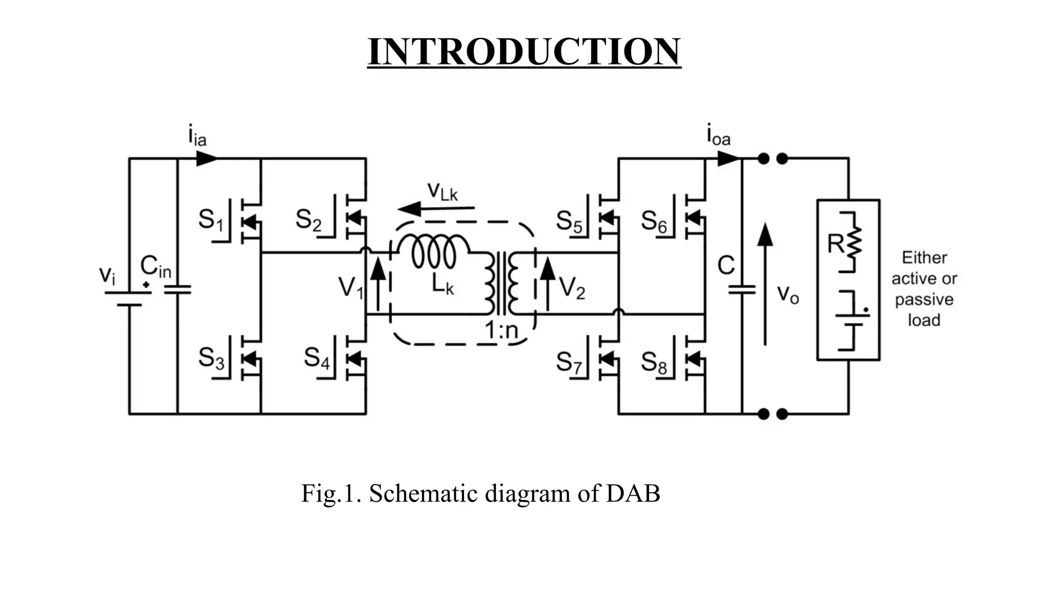
Why DAB?
Capable ofbidirectional power flow.
Isolated, essential in various applications to ensure safety and
protection.
Simple implementation, lower number of passive components.
Zero-voltage-switching (ZVS) characteristics.
It provide a significant amount of power in a relatively compact
size and lightweight design.
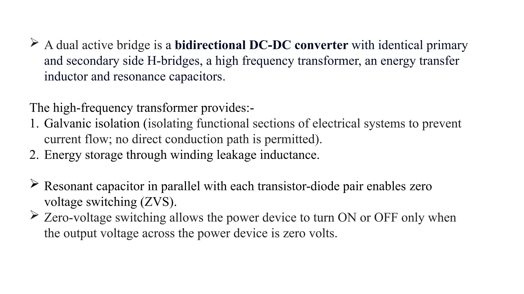
A dualactive bridge is a bidirectional DC-DC converter with identical primary
and secondary side H-bridges, a high frequency transformer, an energy transfer
inductor and resonance capacitors.
The high-frequency transformer provides:-
1. Galvanic isolation (isolating functional sections of electrical systems to prevent
current flow; no direct conduction path is permitted).
2. Energy storage through winding leakage inductance.
Resonant capacitor in parallel with each transistor-diode pair enables zero
voltage switching (ZVS).
Zero-voltage switching allows the power device to turn ON or OFF only when
the output voltage across the power device is zero volts.
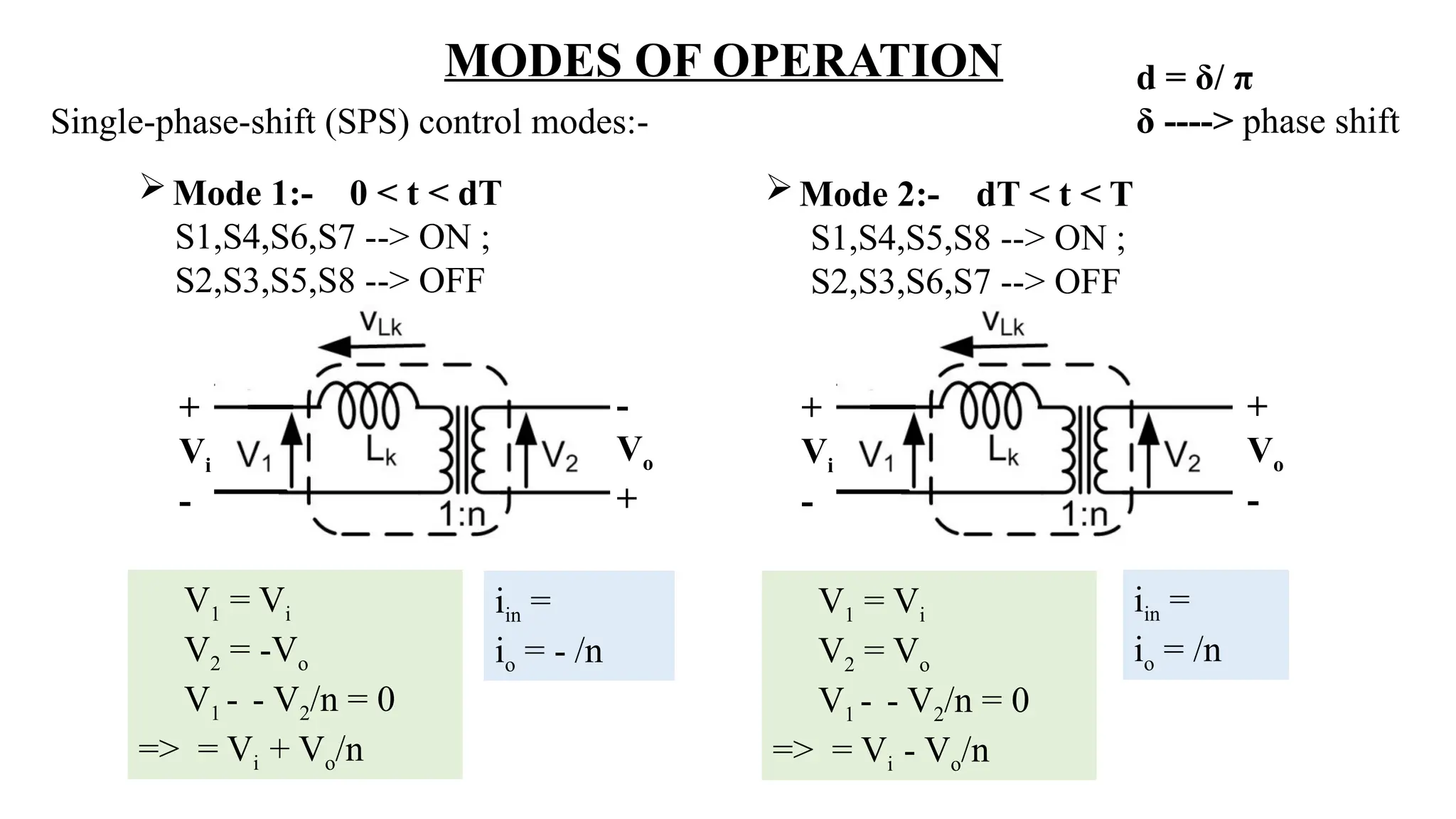
7.
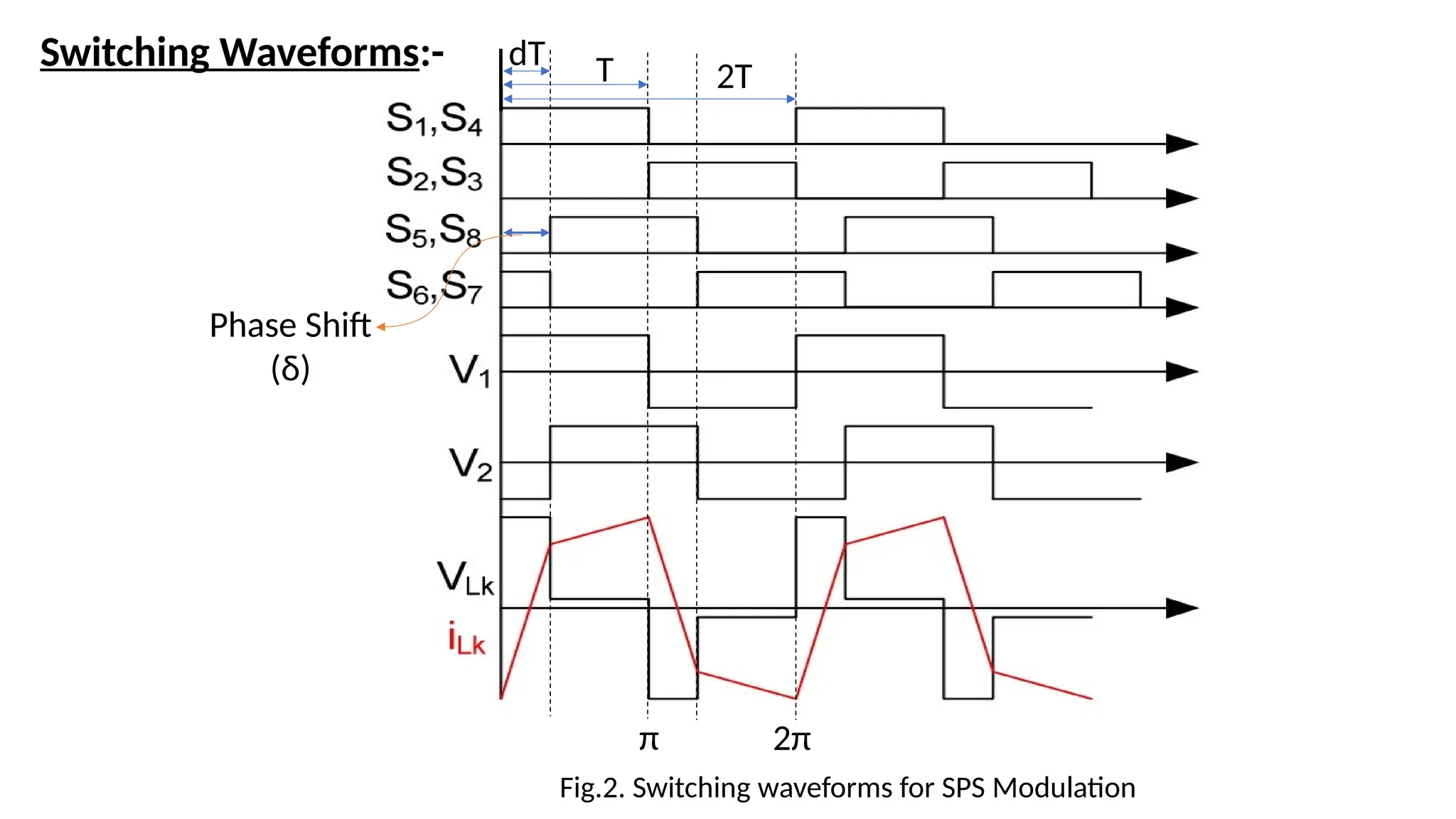
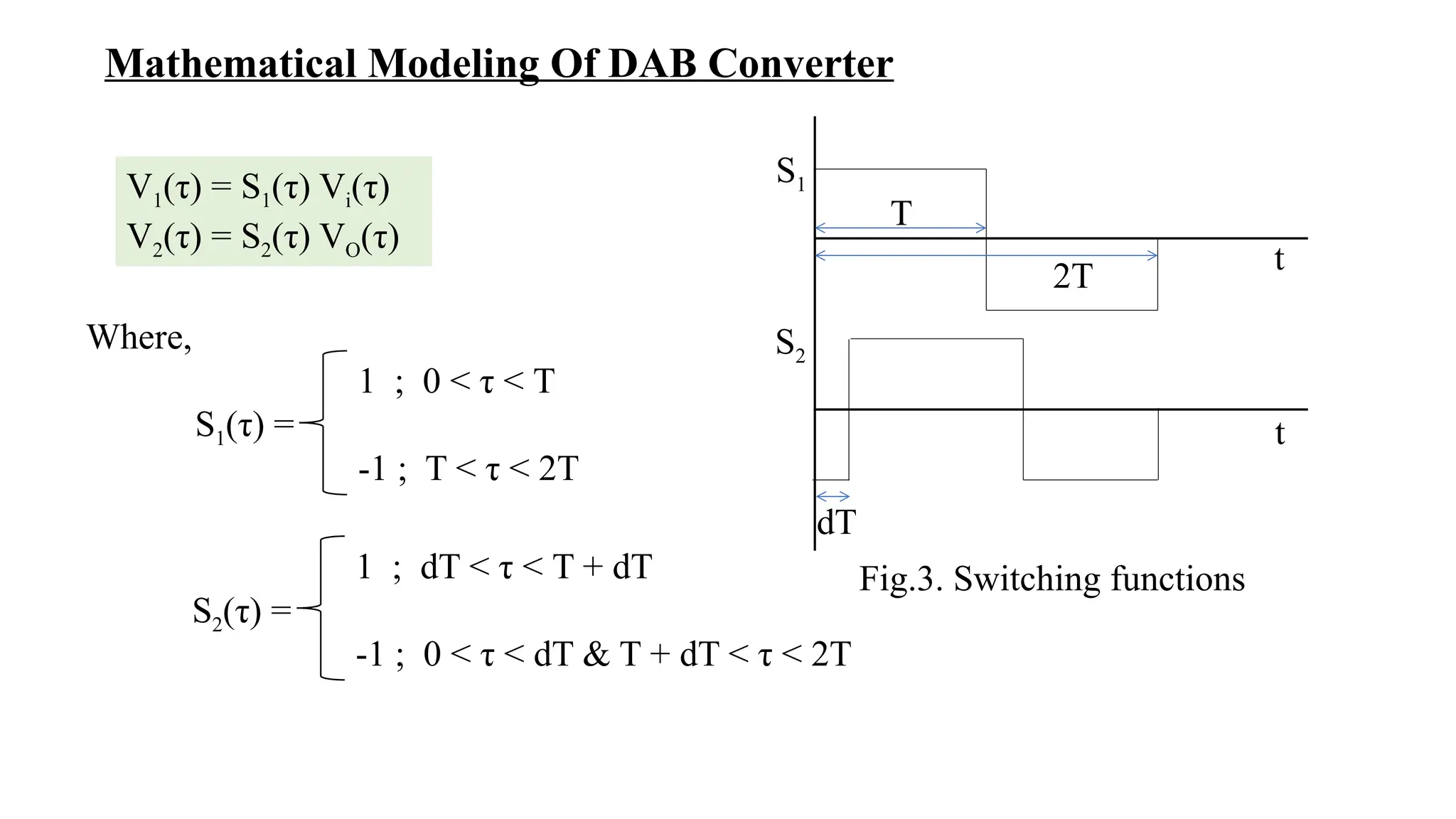
MODES OF OPERATION
Mode1:- 0 < t < dT
S1,S4,S6,S7 --> ON ;
S2,S3,S5,S8 --> OFF
+
Vi
-
-
Vo
+
V1 = Vi
V2 = -Vo
V1 - - V2/n = 0
=> = Vi + Vo/n
Single-phase-shift (SPS) control modes:-
d = δ/ π
δ ----> phase shift
iin =
io = - /n
Mode 2:- dT < t < T
S1,S4,S5,S8 --> ON ;
S2,S3,S6,S7 --> OFF
+
Vi
-
+
Vo
-
V1 = Vi
V2 = Vo
V1 - - V2/n = 0
=> = Vi - Vo/n
iin =
io = /n
8.
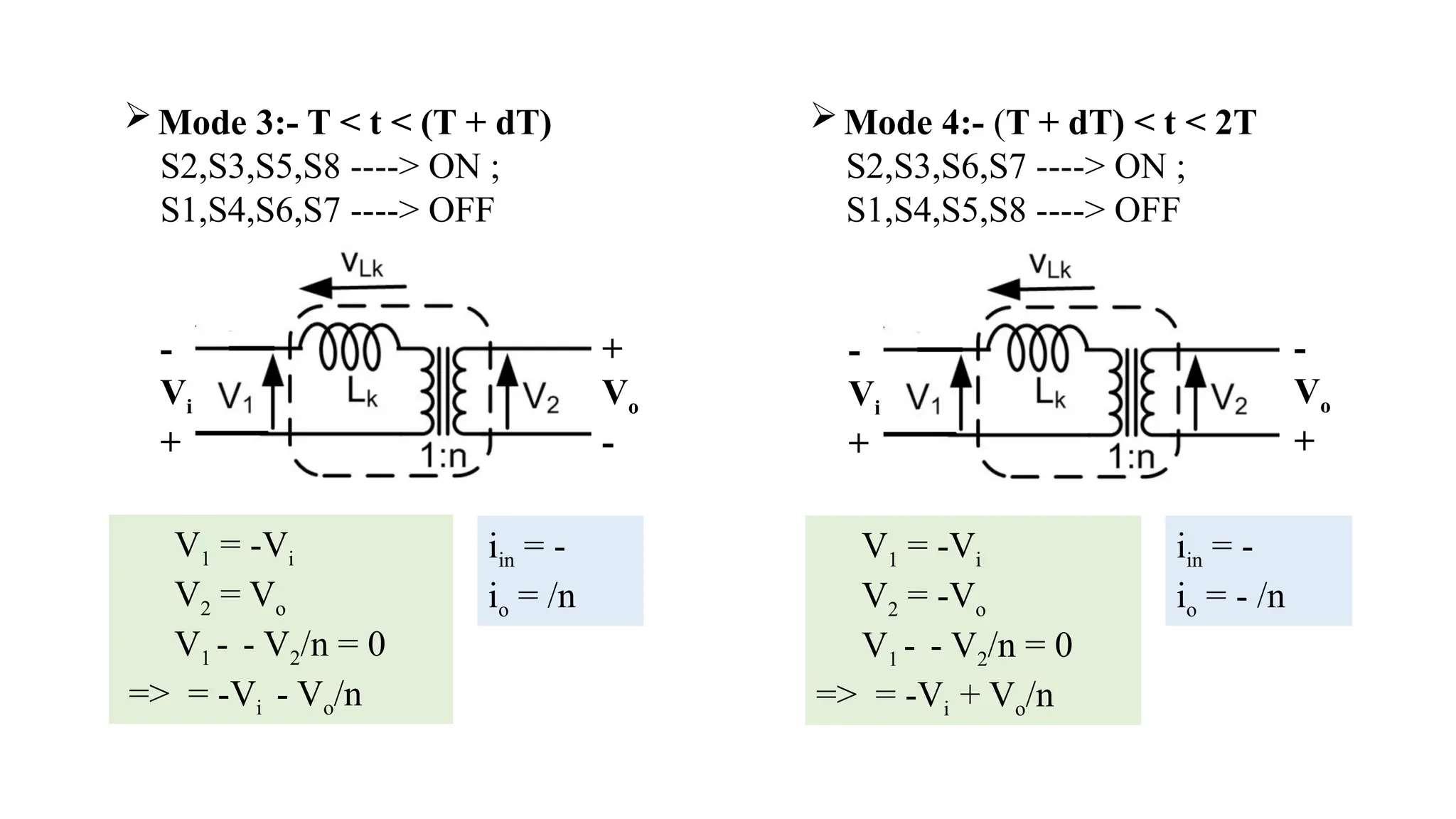
Mode 3:- T< t < (T + dT)
S2,S3,S5,S8 ----> ON ;
S1,S4,S6,S7 ----> OFF
-
Vi
+
+
Vo
-
V1 = -Vi
V2 = Vo
V1 - - V2/n = 0
=> = -Vi - Vo/n
iin = -
io = /n
Mode 4:- (T + dT) < t < 2T
S2,S3,S6,S7 ----> ON ;
S1,S4,S5,S8 ----> OFF
-
Vi
+
-
Vo
+
V1 = -Vi
V2 = -Vo
V1 - - V2/n = 0
=> = -Vi + Vo/n
iin = -
io = - /n
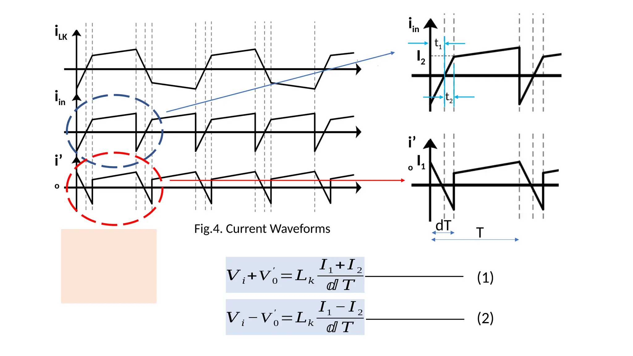
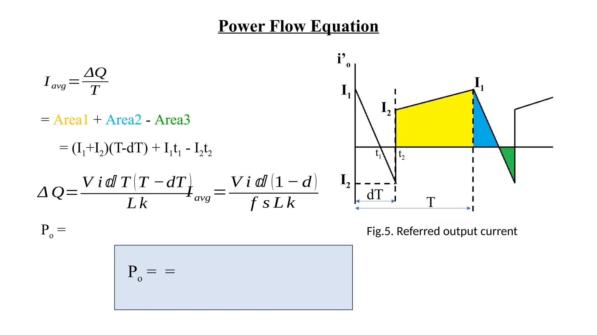
Power Flow Equation
i’o
I1
I2
dT
T
t1t2
Iavg =
ΔQ
T
= Area1 + Area2 - Area3
= (I1+I2)(T-dT) + I1t1 - I2t2
I2
I1
Δ Q=
V i ⅆ T (T −dT )
L k
Iavg =
V i ⅆ (1 − d )
f s L k
Po =
Po = =
Fig.5. Referred output current
15.
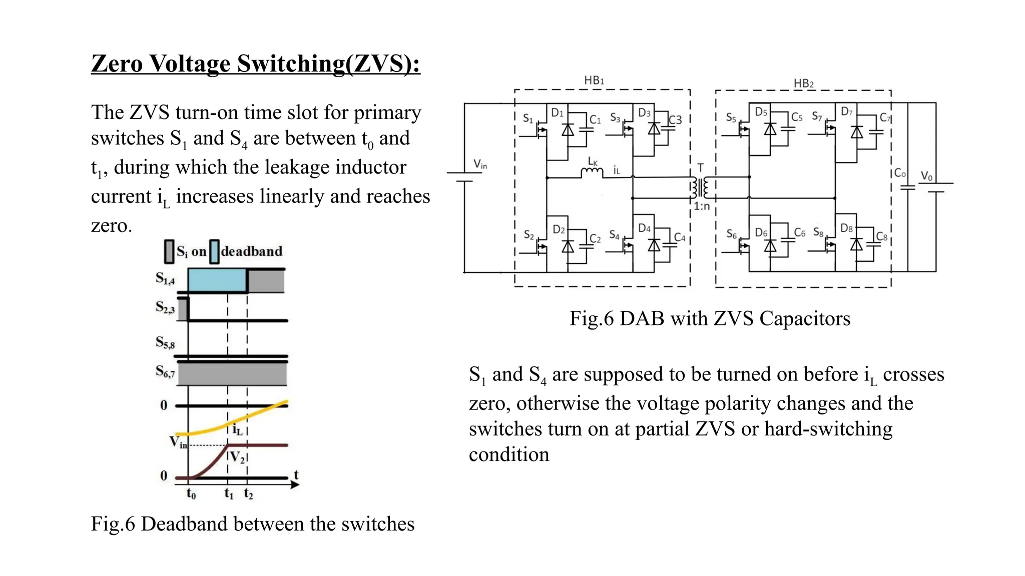
Zero Voltage Switching(ZVS):
TheZVS turn-on time slot for primary
switches S1 and S4 are between t0 and
t1, during which the leakage inductor
current iL increases linearly and reaches
zero.
S1 and S4 are supposed to be turned on before iL crosses
zero, otherwise the voltage polarity changes and the
switches turn on at partial ZVS or hard-switching
condition
Fig.6 DAB with ZVS Capacitors
Fig.6 Deadband between the switches
16.
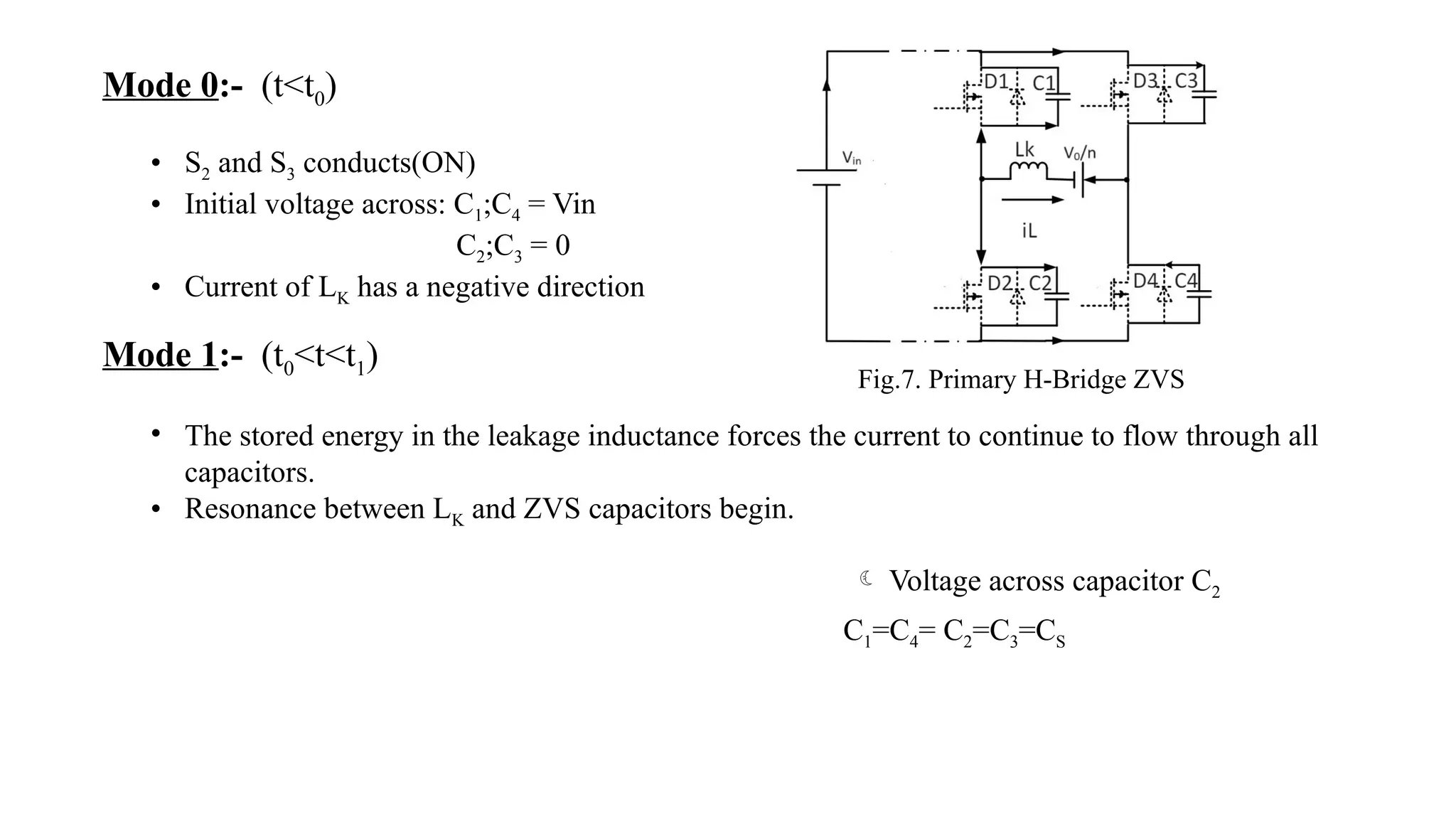
Mode 0:- (t<t0)
•S2 and S3 conducts(ON)
• Initial voltage across: C1;C4 = Vin
C2;C3 = 0
• Current of LK has a negative direction
Mode 1:- (t0<t<t1)
• The stored energy in the leakage inductance forces the current to continue to flow through all
capacitors.
• Resonance between LK and ZVS capacitors begin.
C1=C4= C2=C3=CS
Voltage across capacitor C2
Fig.7. Primary H-Bridge ZVS
17.
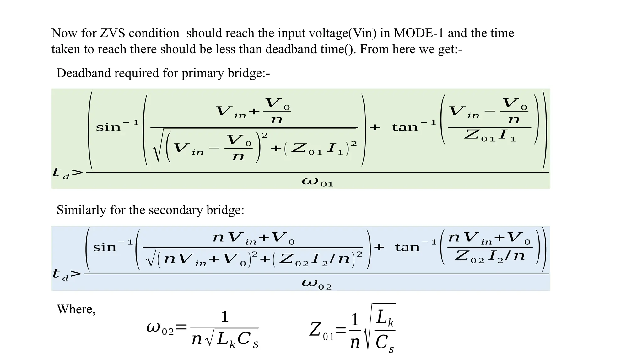
Mode 2:- (t1<t<t2)
Byconducting D1 and D4 the resonance phenomena ends and S1 and S4 can be turned
ON under ZVS condition.
On solving the previous differential equation we get:
Where,
)
I 1 → initial current
18.
𝑡 d >
(sin
−1
(
𝑉 𝑖𝑛 +
𝑉 0
𝑛
√(𝑉 𝑖𝑛 −
𝑉 0
𝑛 )
2
+( 𝑍0 1 𝐼1 )
2
)+ tan
− 1
(𝑉 𝑖𝑛 −
𝑉 0
𝑛
𝑍0 1 𝐼 1
))
𝜔01
Deadband required for primary bridge:-
Now for ZVS condition should reach the input voltage(Vin) in MODE-1 and the time
taken to reach there should be less than deadband time(). From here we get:-
Similarly for the secondary bridge:
𝑡 d >
(sin
− 1
(
𝑛 𝑉 𝑖𝑛+𝑉 0
√( 𝑛𝑉 𝑖𝑛+ 𝑉 0 )
2
+( 𝑍0 2 𝐼 2 / 𝑛)
2
)+ tan
− 1
(𝑛 𝑉 𝑖𝑛+𝑉 0
𝑍0 2 𝐼2 / 𝑛 ))
𝜔0 2
𝜔02=
1
𝑛√𝐿𝑘𝐶S
𝑍01=
1
𝑛 √𝐿𝑘
𝐶𝑠
Where,
19.
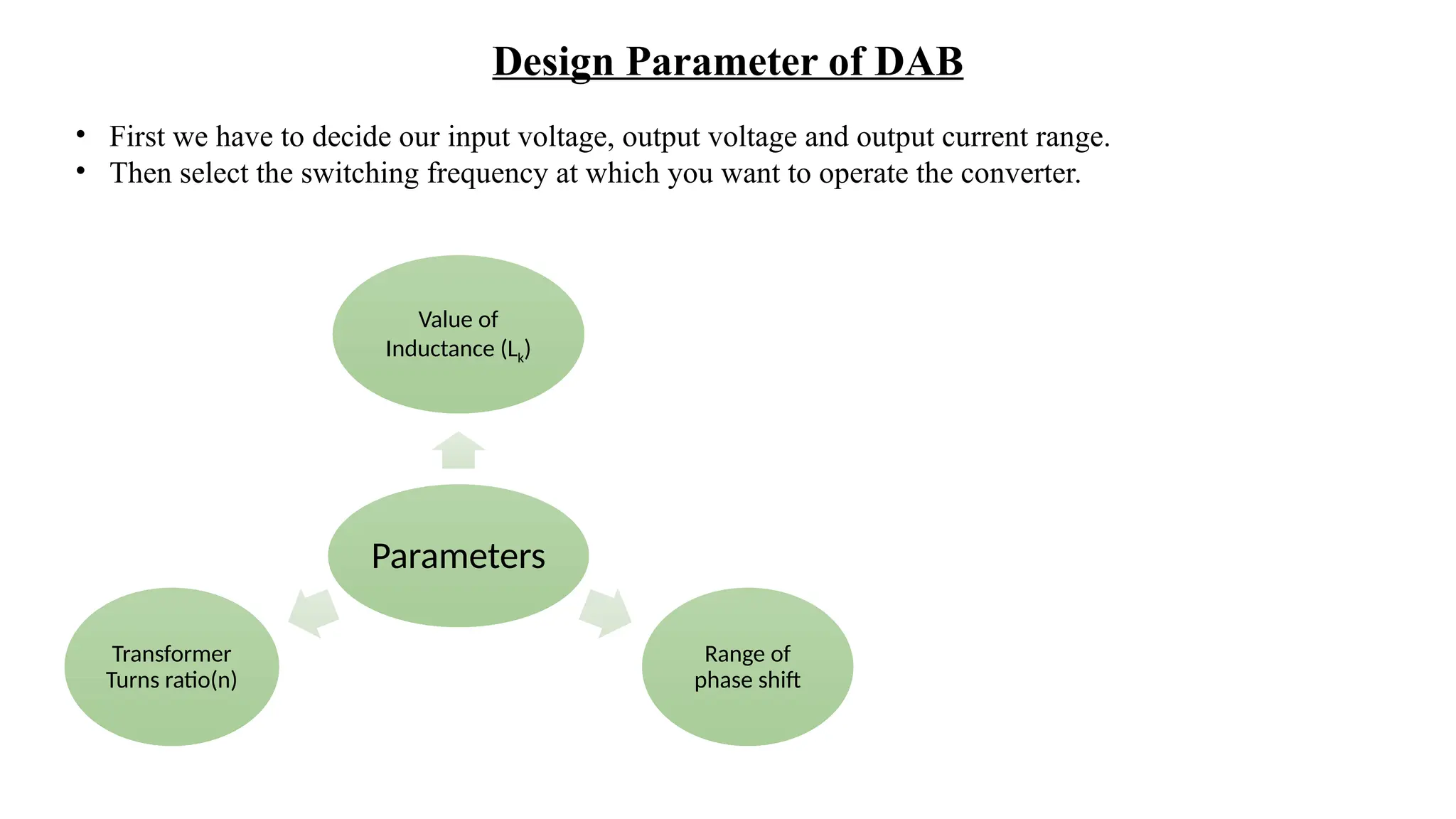
Design Parameter ofDAB
• First we have to decide our input voltage, output voltage and output current range.
• Then select the switching frequency at which you want to operate the converter.
Parameters
Value of
Inductance (Lk)
Range of
phase shift
Transformer
Turns ratio(n)
20.
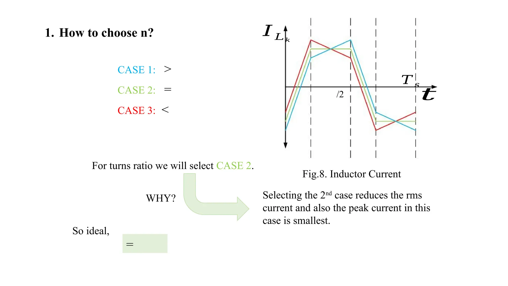
1. How tochoose n?
CASE 1: >
CASE 2: =
CASE 3: <
𝐼 𝐿𝑘
𝑡
/2
𝑇 𝑠
For turns ratio we will select CASE 2.
WHY? Selecting the 2nd
case reduces the rms
current and also the peak current in this
case is smallest.
=
So ideal,
Fig.8. Inductor Current
21.
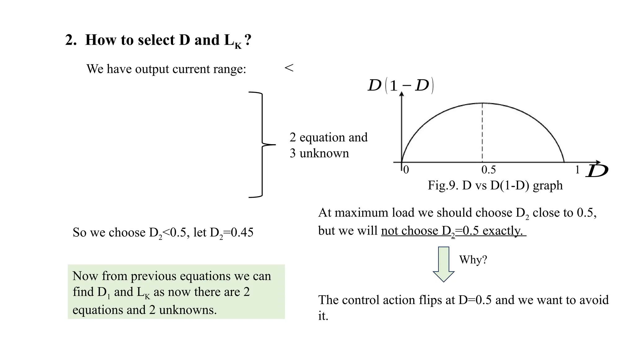
2. How toselect D and LK ?
We have output current range: <
2 equation and
3 unknown
𝐷 (1 − 𝐷)
𝐷
0 0.5 1
At maximum load we should choose D2 close to 0.5,
but we will not choose D2=0.5 exactly.
Why?
The control action flips at D=0.5 and we want to avoid
it.
So we choose D2<0.5, let D2=0.45
Now from previous equations we can
find D1 and LK as now there are 2
equations and 2 unknowns.
Fig.9. D vs D(1-D) graph
22.
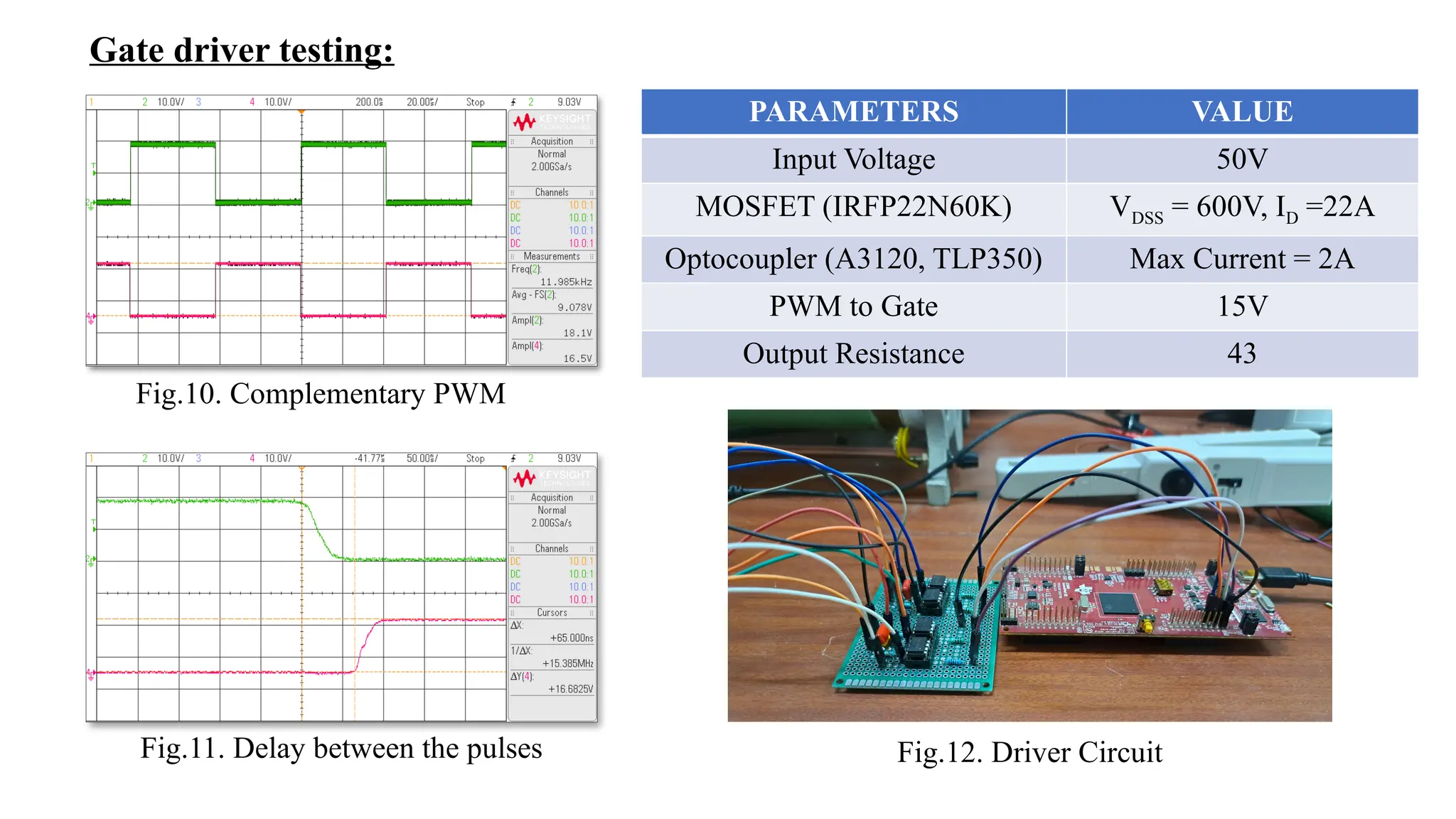
Gate driver testing:
Fig.10.Complementary PWM
Fig.11. Delay between the pulses Fig.12. Driver Circuit
PARAMETERS VALUE
Input Voltage 50V
MOSFET (IRFP22N60K) VDSS = 600V, ID =22A
Optocoupler (A3120, TLP350) Max Current = 2A
PWM to Gate 15V
Output Resistance 43
23.
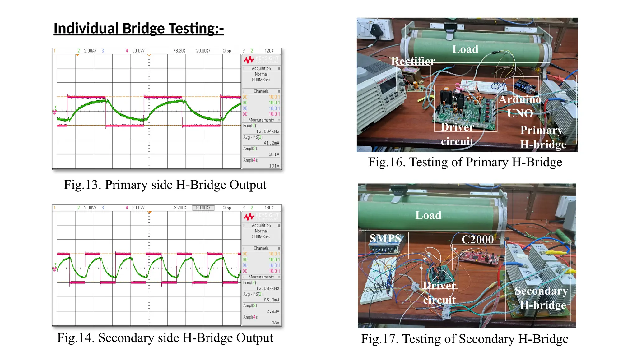
Fig.13. Primary sideH-Bridge Output
Fig.14. Secondary side H-Bridge Output
Load
Secondary
H-bridge
Driver
circuit
SMPS C2000
Fig.16. Testing of Primary H-Bridge
Fig.17. Testing of Secondary H-Bridge
Rectifier
Load
Driver
circuit
Arduino
UNO
Primary
H-bridge
Individual Bridge Testing:-
24.
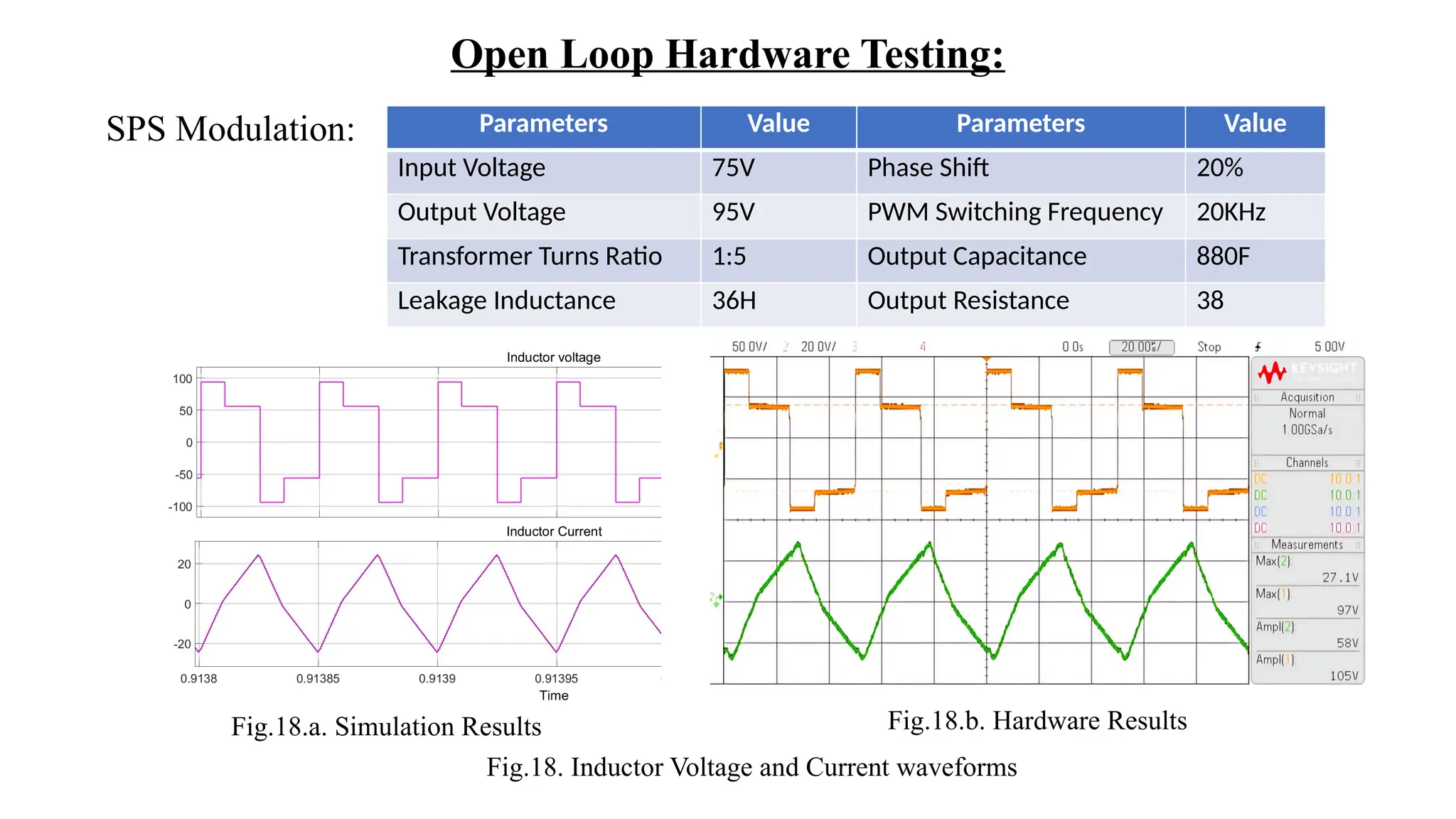
Open Loop HardwareTesting:
SPS Modulation: Parameters Value Parameters Value
Input Voltage 75V Phase Shift 20%
Output Voltage 95V PWM Switching Frequency 20KHz
Transformer Turns Ratio 1:5 Output Capacitance 880F
Leakage Inductance 36H Output Resistance 38
Fig.18.b. Hardware Results
Fig.18.a. Simulation Results
Fig.18. Inductor Voltage and Current waveforms
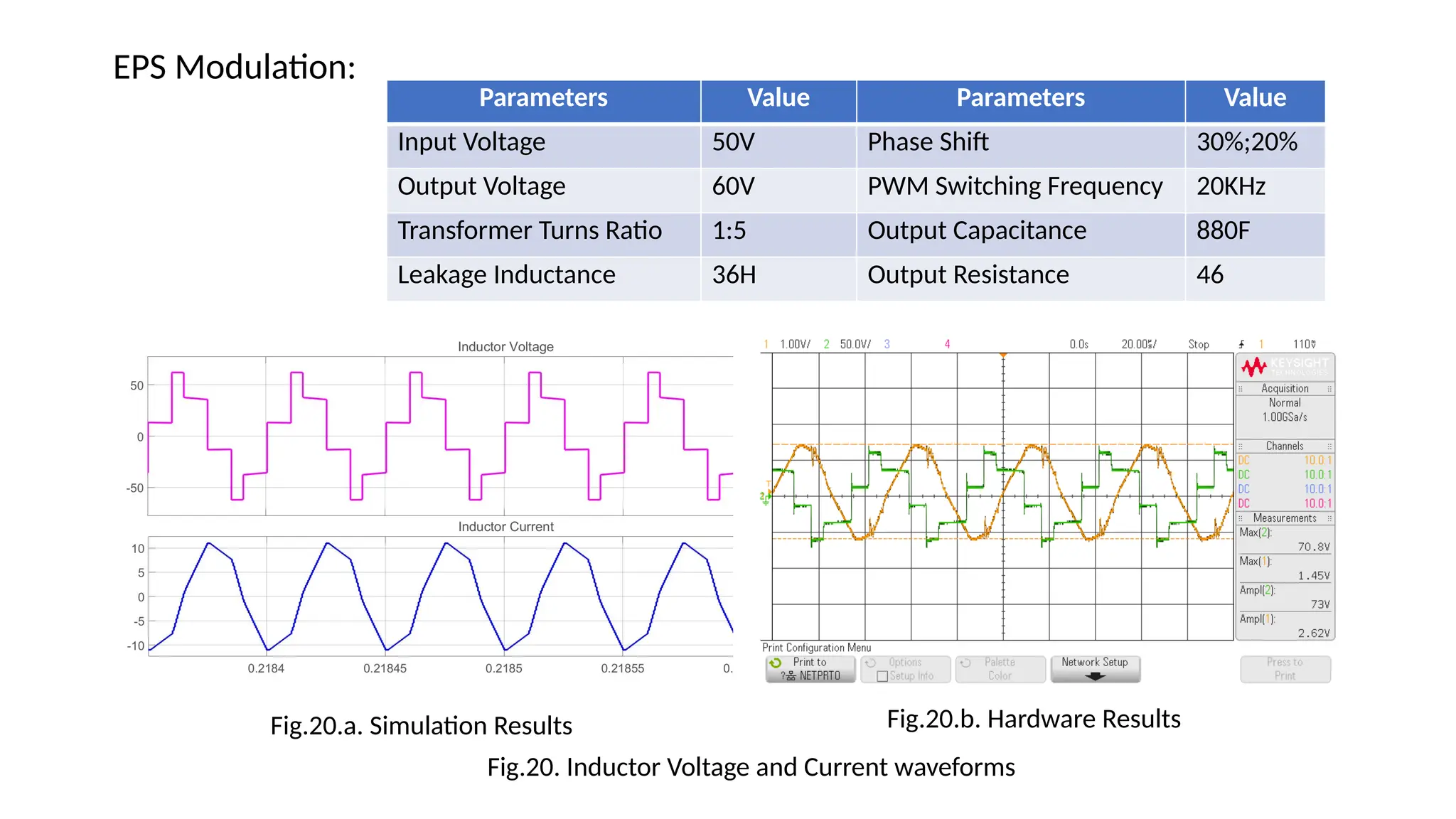
EPS Modulation:
Parameters ValueParameters Value
Input Voltage 50V Phase Shift 30%;20%
Output Voltage 60V PWM Switching Frequency 20KHz
Transformer Turns Ratio 1:5 Output Capacitance 880F
Leakage Inductance 36H Output Resistance 46
Fig.20.a. Simulation Results Fig.20.b. Hardware Results
Fig.20. Inductor Voltage and Current waveforms
27.
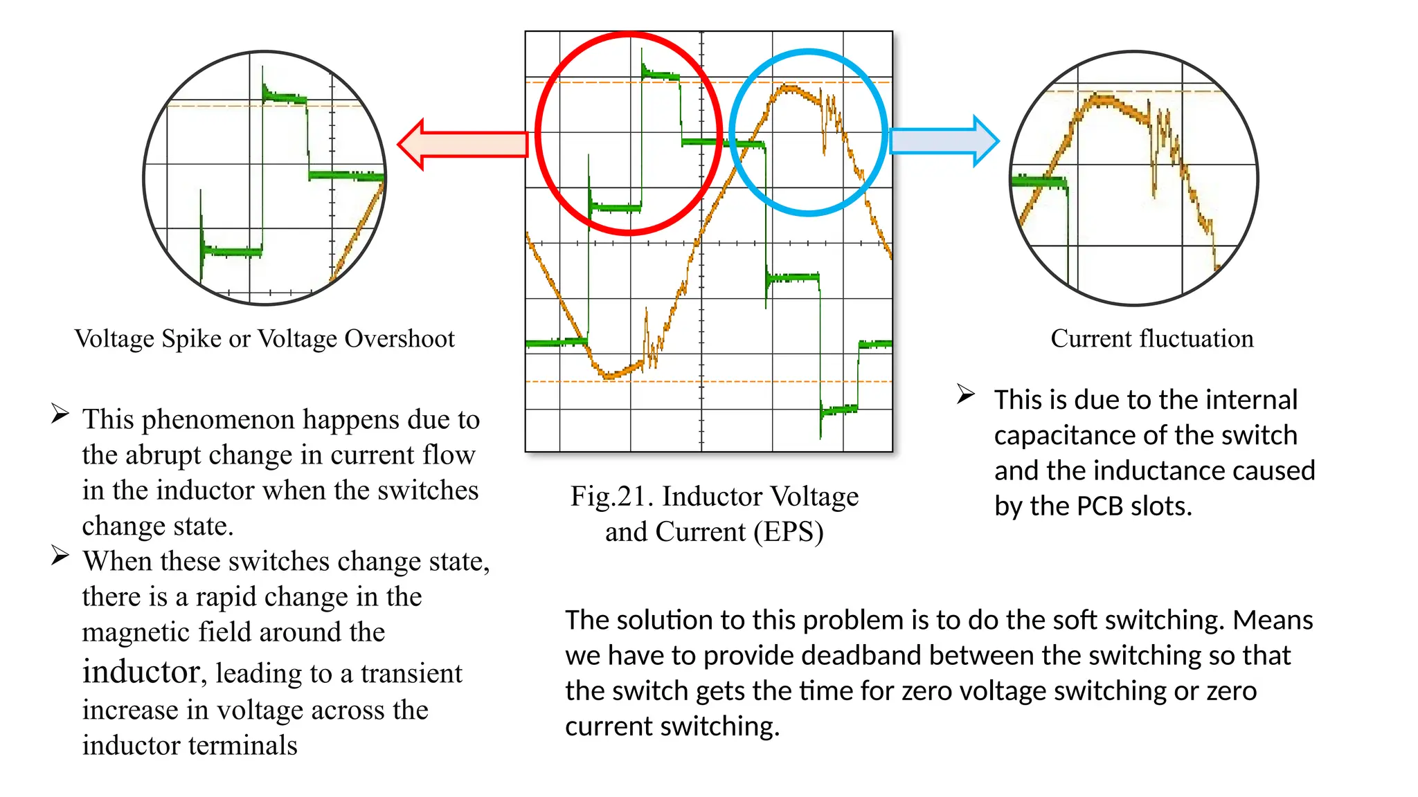
Voltage Spike orVoltage Overshoot
This phenomenon happens due to
the abrupt change in current flow
in the inductor when the switches
change state.
When these switches change state,
there is a rapid change in the
magnetic field around the
inductor, leading to a transient
increase in voltage across the
inductor terminals
Current fluctuation
Fig.21. Inductor Voltage
and Current (EPS)
This is due to the internal
capacitance of the switch
and the inductance caused
by the PCB slots.
The solution to this problem is to do the soft switching. Means
we have to provide deadband between the switching so that
the switch gets the time for zero voltage switching or zero
current switching.
28.
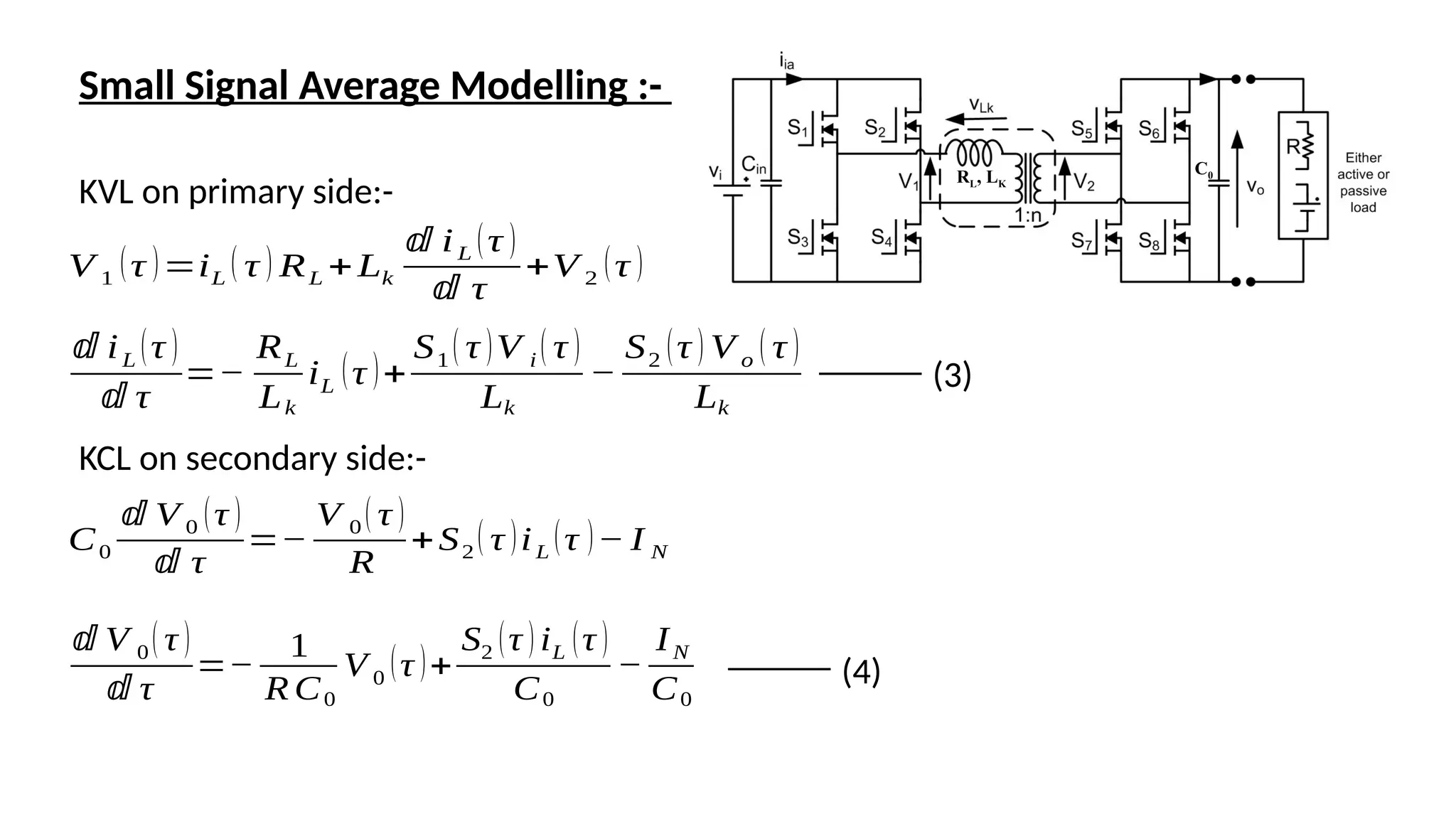
Small Signal AverageModelling :-
KVL on primary side:-
V 1
(τ )=iL
( τ ) RL +Lk
ⅆ iL (τ )
ⅆ τ
+V 2
(τ )
ⅆ iL (τ )
ⅆ τ
=−
RL
Lk
iL
(τ )+
S1 ( τ )V i ( τ )
Lk
−
S2 (τ ) V o ( τ )
Lk
KCL on secondary side:-
C0
ⅆ V 0 (τ )
ⅆ τ
=−
V 0 ( τ )
R
+S2
( τ )iL
(τ )− I N
ⅆ V 0( τ )
ⅆ τ
=−
1
R C0
V 0
(τ )+
S2 (τ ) iL (τ )
C0
−
IN
C0
(3)
(4)
RL, LK
C0
29.
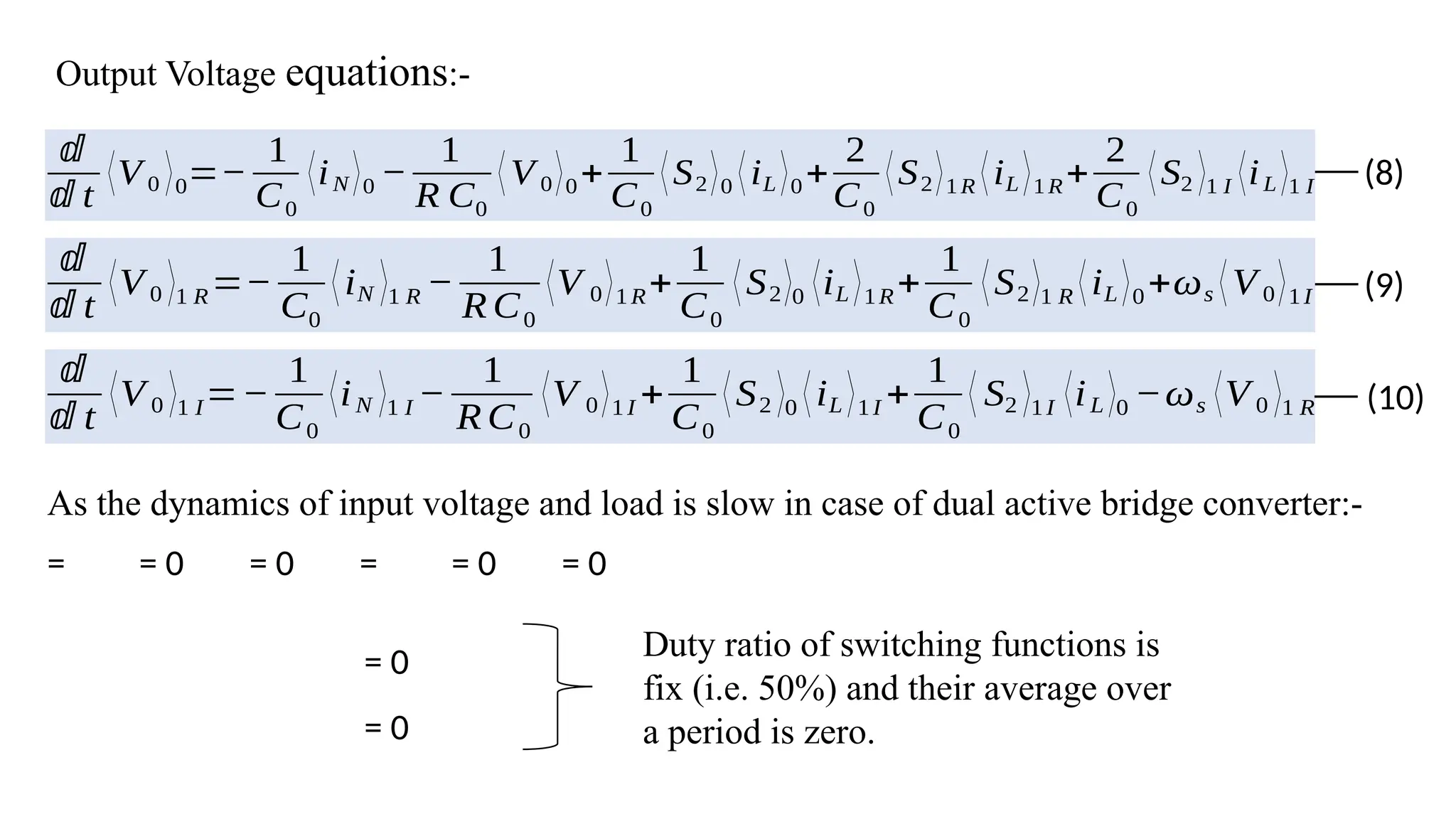
Generalized averaging:
x (τ)=∑
k=− ∞
∞
⟨x⟩k (t)ejk ωs τ
⟨ x⟩k (t)=
1
2T
∫
t−2T
t
x (τ)e
− jk ωsτ
ⅆ τ
Properties of Fourier series:-
1. =
2. =
3. = *
+ 2{ +
+ j
Where,
= +
= +
State variable
Kth
coefficient of
Fourier series
ⅆ
ⅆ t
⟨V 0⟩0=−
1
C0
⟨iN ⟩0 −
1
R C0
⟨V 0⟩0+
1
C0
⟨S2⟩0 ⟨iL ⟩0+
2
C0
⟨S2⟩1R ⟨iL ⟩1R+
2
C0
⟨S2 ⟩1 I ⟨iL ⟩1 I
ⅆ
ⅆ t
⟨V 0 ⟩1 R=−
1
C0
⟨iN ⟩1 R −
1
R C0
⟨V 0⟩1R+
1
C0
⟨S2⟩0 ⟨iL ⟩1R+
1
C0
⟨S2⟩1 R ⟨iL ⟩0+ωs ⟨V 0⟩1I
ⅆ
ⅆ t
⟨V 0 ⟩1 I=−
1
C0
⟨iN ⟩1 I −
1
R C0
⟨V 0⟩1I +
1
C0
⟨S2 ⟩0 ⟨iL ⟩1I +
1
C0
⟨ S2 ⟩1I ⟨iL ⟩0 −ωs ⟨V 0 ⟩1 R
Output Voltage equations:-
(8)
(9)
(10)
As the dynamics of input voltage and load is slow in case of dual active bridge converter:-
= = 0 = 0 = = 0 = 0
= 0
= 0
Duty ratio of switching functions is
fix (i.e. 50%) and their average over
a period is zero.
32.
⟨ S1 ⟩k=
1
2Tk ωs
{[2sin (k T ωs)−sin (2kT ωs)]+ j[2cos(kT ωs)− cos(2 kT ωs)−1]} (11)
(12)
Switching function equations:-
From eq. (11) and eq. (12) we get:-
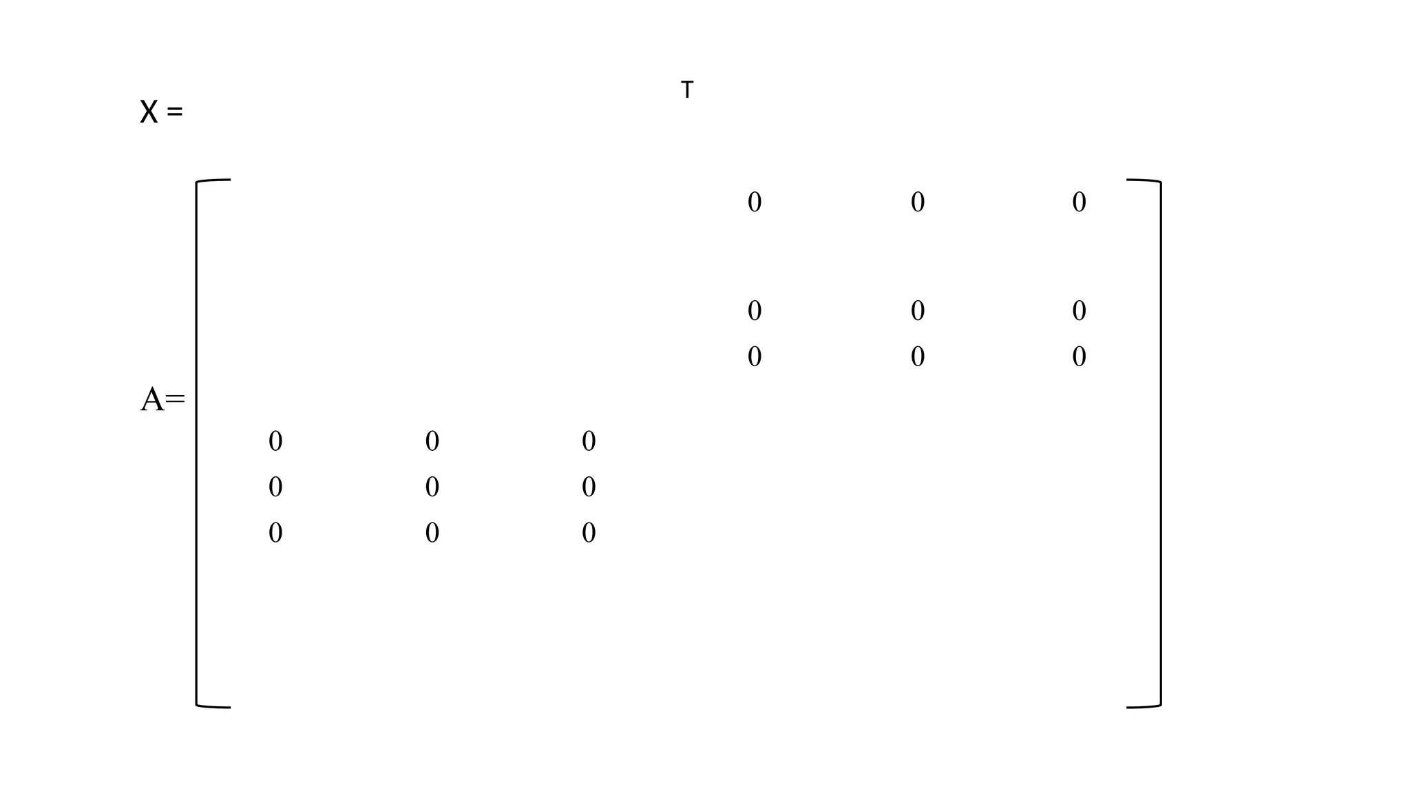
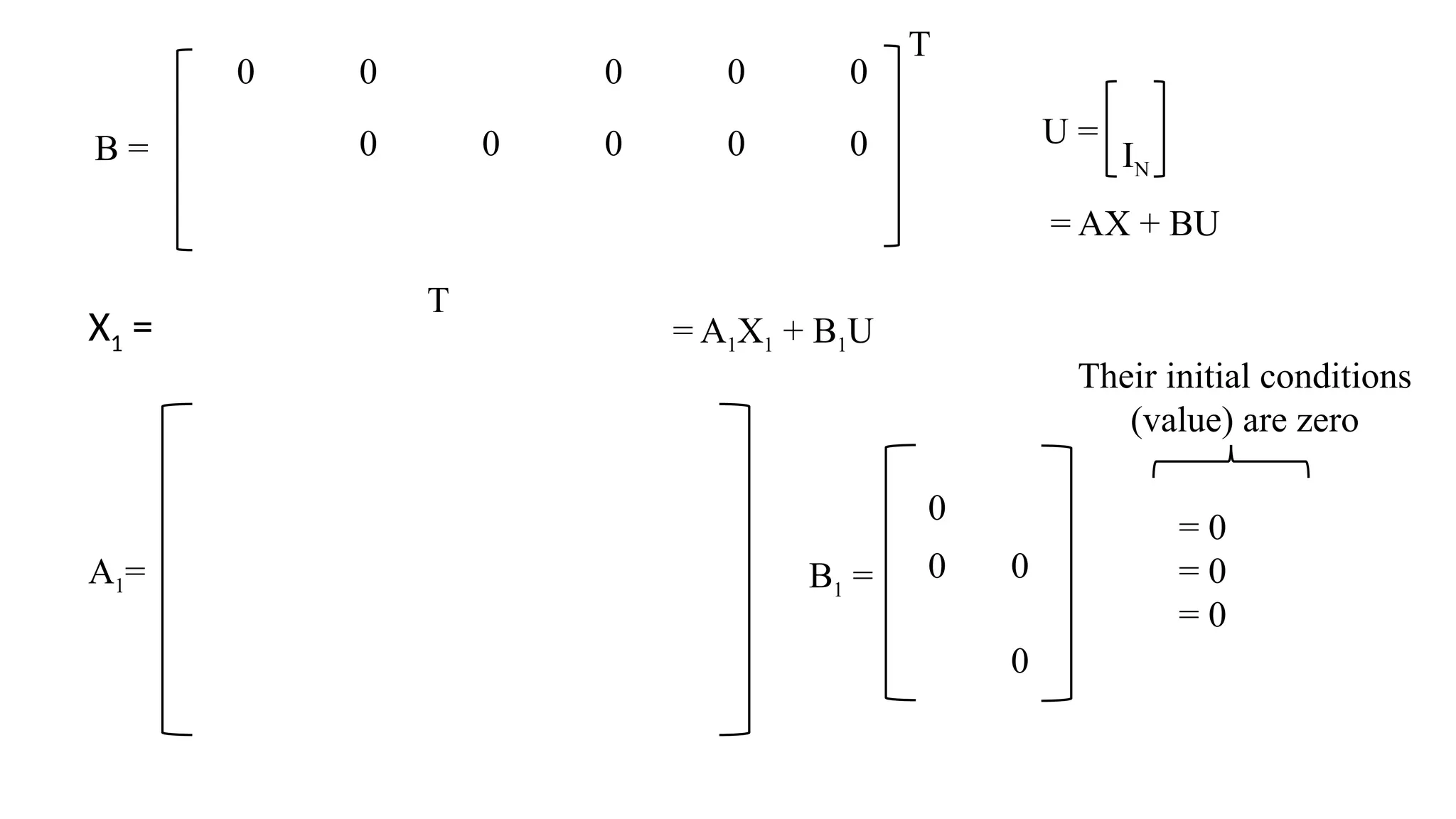
B = IN
U=
= AX + BU
= 0
= 0
= 0
Their initial conditions
(value) are zero
A1=
0
0 0
0
B1 =
0 0 0 0 0
0 0 0 0 0
T
X1 =
T
= A1X1 + B1U
35.
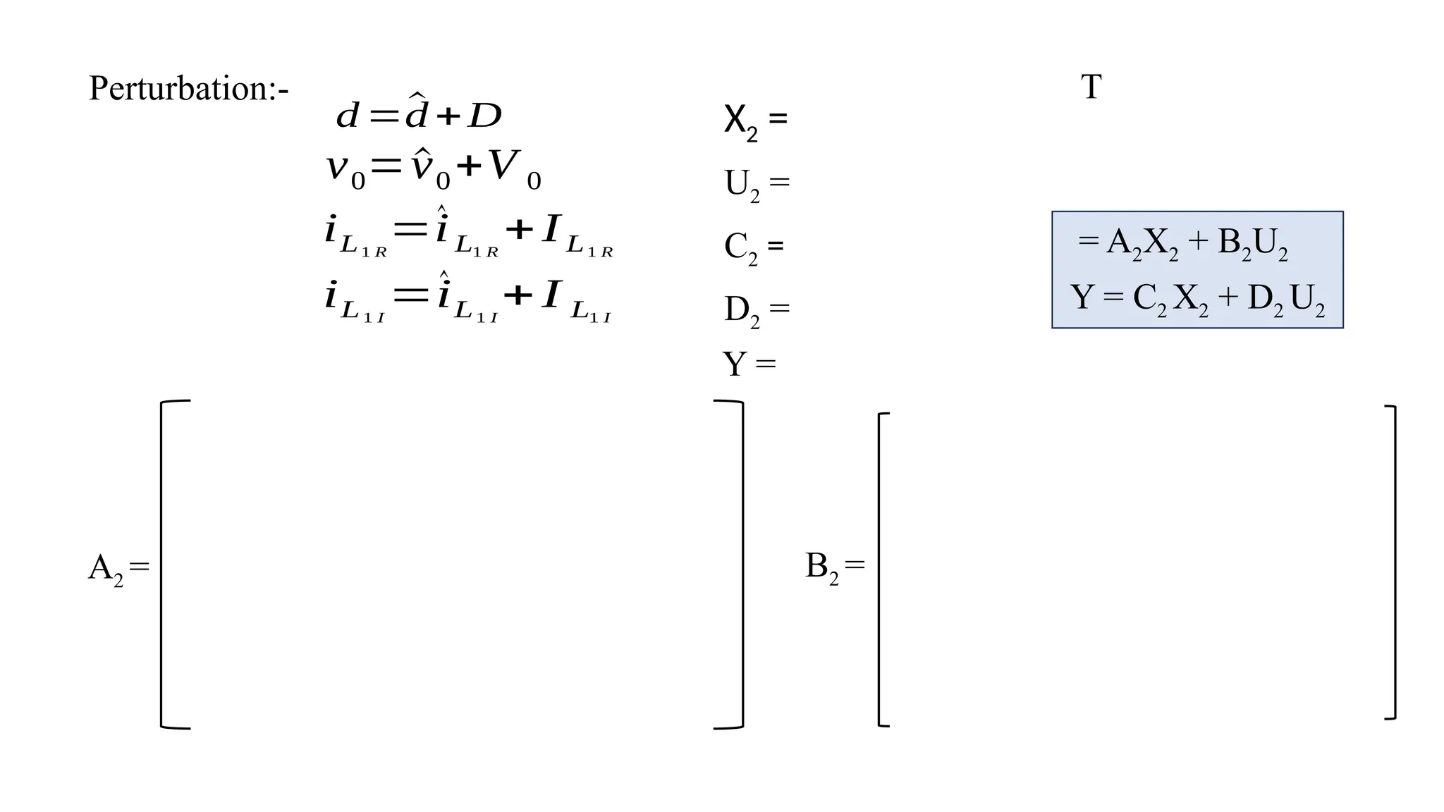
Perturbation:-
d =^
d +D
v0=^
v0+V 0
iL1 R
=^
iL1 R
+IL1 R
iL1 I
=^
iL1 I
+ I L1 I
X2 =
T
A2 =
U2 =
= A2X2 + B2U2
C2 =
D2 = Y = C2 X2 + D2 U2
Y =
B2 =
36.
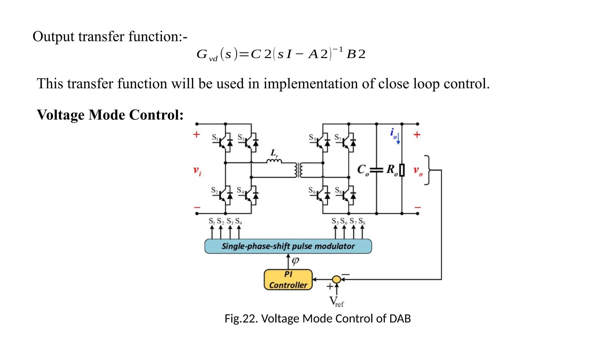
Output transfer function:-
Gvd(s)=C 2( s I − A 2)−1
B 2
This transfer function will be used in implementation of close loop control.
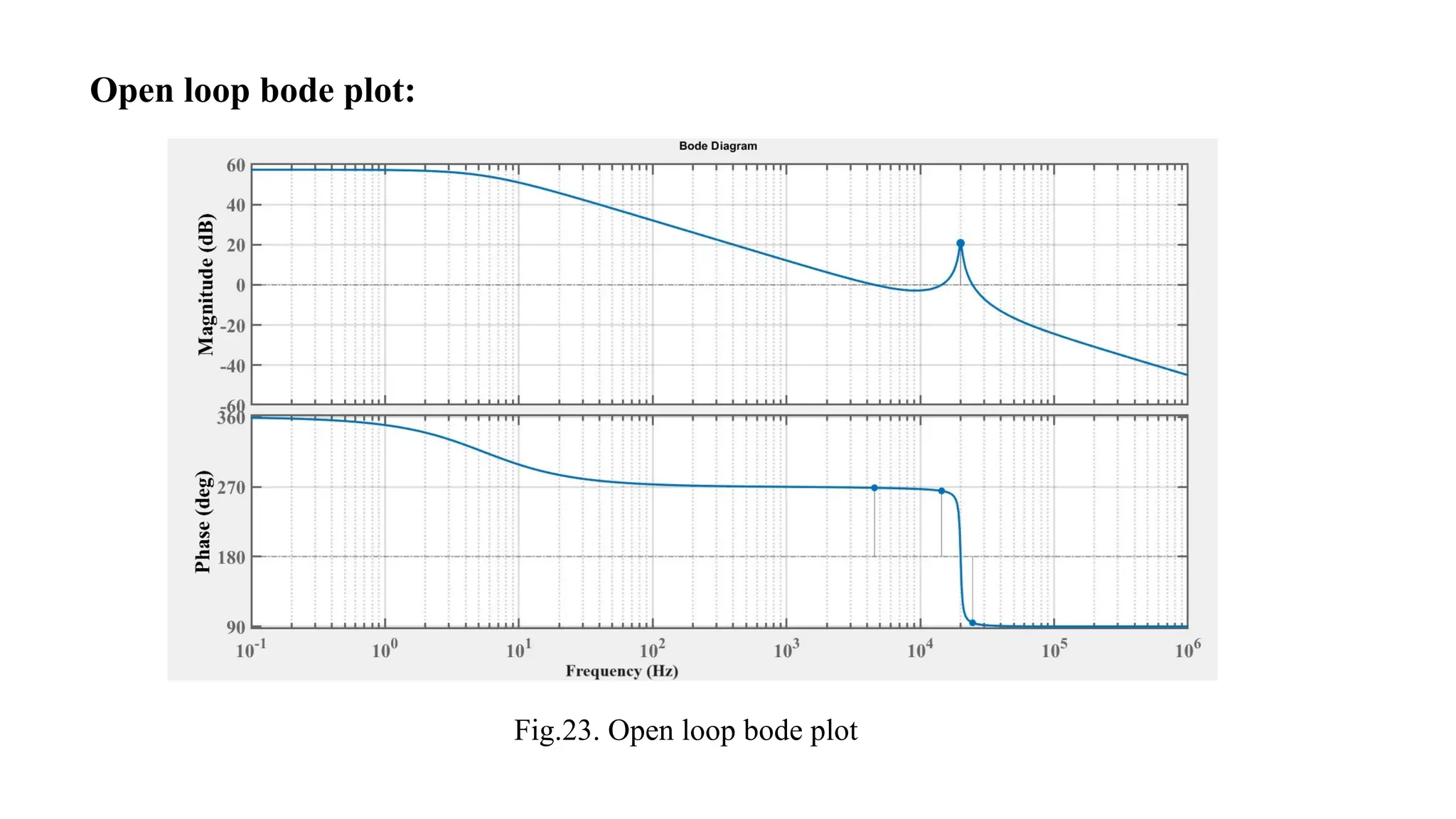
Voltage Mode Control:
Fig.22. Voltage Mode Control of DAB
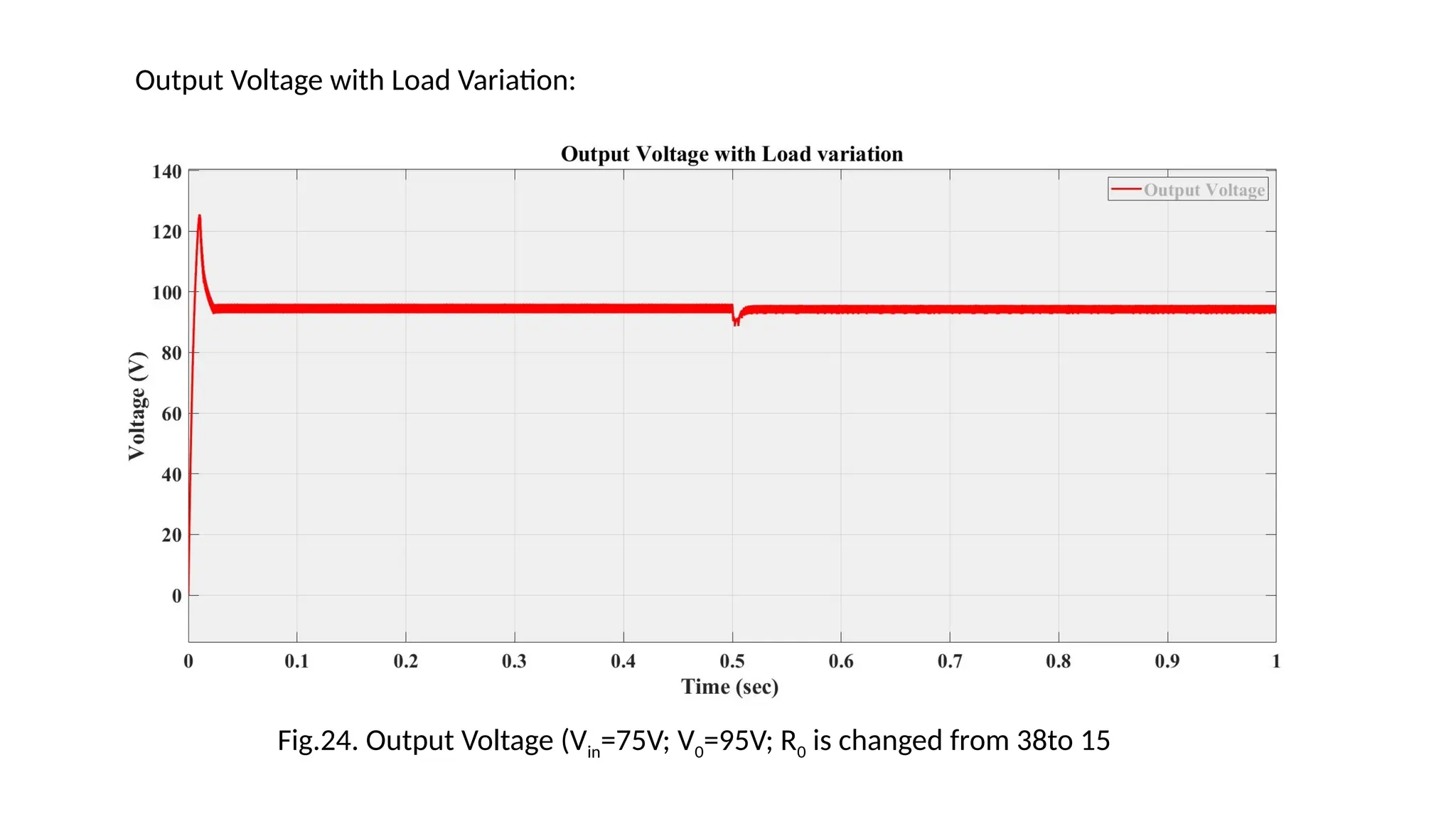
Output Voltage withLoad Variation:
Fig.24. Output Voltage (Vin=75V; V0=95V; R0 is changed from 38to 15
39.
Conclusion:
• Working ofDAB converter and all the modes of operation have been understand.
• Power flow equation has been derived.
• Zero Voltage Switching conditions have been derived and implemented.
• Hardware implementation has been done using different modulation techniques.
• Small signal Analysis and Close loop control has been done.
DAB can be used in many application that requires bidirectional power flow and also in
between the grid and other applications that requires DC DC convertion.
40.
REFERENCES
1. H. Qinand J.W. Kimball, “Generalized average modeling of dual active bridge DC-DC converter,”
IEEE Trans. on Power Elec., vol. 27, no. 4, pp. 2078-2084, April 2012.
2. B. Zhao, Q. Song, W. Liu and Y. Sun, “Overview of Dual-Active-Bridge Isolated Bidirectional DC-
DC Converter for High-Frequency-Link Power Conversion System,” IEEE Trans. on Power Elec.,
vol. 29, no. 8, pp. 4091-4106, Aug. 2014.
3. H. Qin and J. W. Kimball, "Closed-loop control of DC-DC dual-active bridge converters driving
single-phase inverter", IEEE Trans. Power Electron., vol. 29, no. 2, pp. 1006-1017, Feb. 2014.
4. F. Krismeri, S. Round and J.W. Kolar, “Performance optimization of a high current dual active
bridge with a wide operating voltage range,” in: 37th IEEE Power Electronics Specialists
Conference, Jeju, South Korea, June, 18-22,2006, pp. 1-7.
5. S.R. Sanders, J.M. Noworolski, X.Z. Liu and G.C. Verghese, “Generalized averaging method for
power conversion circuits,” IEEE Trans on Power Elec., vol. 6, no. 2, pp. 251-259, April 1991.
6. J.A. Mueller and J.W. Kimball, “An improved generalized average model of DC-DC dual active
bridge converters,” IEEE Trans. on Power Elec. vol. 33, no. 11, pp. 9975-9988, Nov. 2018.
7. M. N. Kheraluwala, R. W. Gascoigne, D. M. Divan, and E. D. Baumann, “Performance
characterization of a high-power dual active bridge,” IEEE Trans. Ind. Appl., vol. 28, no. 6, pp.
1294–1301, 1992.


![⟨ S1 ⟩k =
1
2Tk ωs
{[2sin (k T ωs)−sin (2kT ωs)]+ j[2cos(kT ωs)− cos(2 kT ωs)−1]} (11)
(12)
Switching function equations:-
From eq. (11) and eq. (12) we get:-](https://image.slidesharecdn.com/rp-2dab-240810131337-ab0b2e3a/75/Dual-Active-Bridge-Converter-a-Bidirectional-Isolated-DC-DC-Converter-32-2048.jpg)