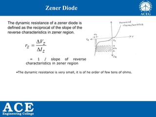
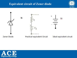
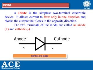
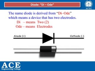
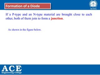
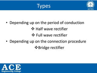
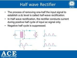
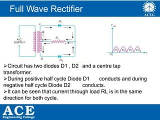
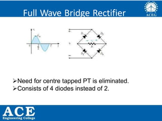
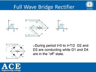
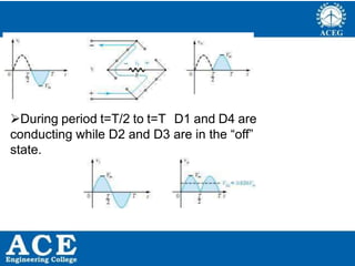
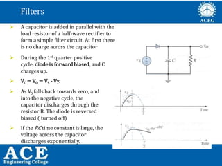
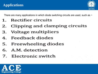
Varactor diode is a type of PN junction diode where the capacitance of the PN junction can be controlled by applying a reverse bias voltage. As the reverse bias voltage is changed, the width of the depletion region between the P and N semiconductors changes, altering the capacitance. Varactor diodes are commonly used in applications like variable resonant tank circuits, automatic frequency control circuits, and frequency modulation in radios and televisions. They operate by varying the capacitance through adjustment of the depletion region width, similar to how the distance between capacitor plates controls capacitance.
Diodes and its application encapsulate the different characteristics of different type of diodes. Also, define its different biases and how it works.
It provides shortcut method in analyzing Clamper and clipper.
At the end of the powerpoint, there has a review question to answer with answer key provided.
Thyristors require commutation to turn off, which involves reducing the anode current to zero and then applying a reverse voltage for a time. There are natural and forced commutation methods. Forced methods include classes A through F, which use resonant circuits, auxiliary thyristors, or line voltage reversals to commutate the main thyristor. Turn off time has two stages - reverse recovery time to remove outer layer carriers, then gate recovery time for inner layer recombination. Proper commutation circuit design is needed to apply reverse voltage for longer than the thyristor's turn off time.
The document discusses diodes, including their history and components. It describes how a diode is constructed from a P-type and N-type semiconductor material, forming a PN junction. At the junction, electrons diffuse into holes, creating a depletion region that acts as an insulator under reverse bias but allows current to flow under forward bias. The document outlines diode applications such as rectification in power supplies and their characteristic I-V curve.
Clampers are electronic circuits that shift a waveform to a different voltage level without changing its appearance. There are two main types: positive clampers shift the input signal in a positive direction above a reference level, while negative clampers shift it in a negative direction below the reference. Clampers work by using diodes and capacitors to either pass or block portions of the input signal depending on its polarity, resulting in the output being shifted to a different DC level from the input but retaining the same AC waveform. They are commonly used in applications like test equipment, radar, sonar, and television receivers.
Clipper circuits are used to remove parts of a signal that are above or below a defined reference level. There are several types of clipper circuits: unbiased positive and negative clippers which clip either the positive or negative portions of a signal, and biased positive and negative clippers which use an external bias voltage to adjust the clipping level. Unbiased clippers cut off either the positive or negative half of the input waveform based on the diode configuration. Biased clippers allow changing the clipping level by adjusting the bias voltage applied in series with the input signal and diode.
Tunnel diodes are heavily doped PN junction diodes that exhibit negative resistance. They were invented in 1958 by Dr. Leo Esaki and operate based on the quantum mechanical principle of tunneling. When forward biased, the current initially increases with voltage but then decreases as the voltage is further increased, demonstrating the unique property of negative resistance. Tunnel diodes find application in ultrafast switching, memory storage, satellite communication equipment, and oscillators due to their negative resistance characteristic.
Original Uni-junction transistor or UJT is a simple device in which a bar of N-type semiconductor material into which P-type material is diffused; somewhere along its length defining the device parameter as intrinsic standoff. The 2N2646 is the most commonly used version of UJT.
This document provides an overview of basic electronics concepts including lattices, semiconductors, diodes, and transistors. It begins by defining lattices and their applications in mathematics. It then discusses superconductors, insulators, intrinsic and extrinsic semiconductors, and the band theory of conduction. Diodes and rectifiers are introduced, including half-wave and full-wave rectification circuits. The document concludes by explaining transistors, including bipolar junction transistors with npn and pnp configurations and their characteristics curves. Transistors are shown to have applications as amplifiers and switches in devices like LED spotlights and single transistor radios.
The document discusses different types of power supplies including regulated, unregulated, offline UPS, online UPS, and switch mode power supplies (SMPS). It explains that regulated power supplies use voltage regulating devices like zener diodes or transistors to maintain a constant output voltage regardless of input or load variations. Unregulated supplies do not have this regulation and output voltage fluctuates with input/load. It also compares offline and online UPS configurations and their advantages. Finally, it provides a brief overview of how SMPS work and their benefits over linear power supplies.
Bipolar junction transistors (BJTs) are three-terminal semiconductor devices consisting of two pn junctions. There are two types, NPN and PNP, depending on the order of doping. BJTs can operate as amplifiers and switches by controlling the flow of majority charge carriers through the base terminal. Proper biasing is required to operate the transistor in its active region between cutoff and saturation. Common configurations include common-base, common-emitter, and common-collector, each with different input and output characteristics. Maximum ratings like power dissipation and voltages must be considered for circuit design and temperature derating.
The MOSFET is a four-terminal semiconductor device used for switching and amplifying electronic signals. It comes in two basic forms, P-channel and N-channel, and two modes, depletion and enhancement. MOSFETs exhibit three operating regions - cut-off, where no current flows; ohmic or linear, where current increases with drain-source voltage; and saturation, where current reaches a maximum. MOSFETs are voltage-controlled, unipolar devices that can switch or amplify depending on their operating region.
The document discusses different types of choppers, which are static devices that produce a variable DC voltage from a constant DC source. It describes step-down and step-up choppers and the principles of their operation. Various chopper control methods and classifications are covered, including Class A through Class E choppers and their characteristics. Load and source inductance effects are also summarized.
This document discusses DIACs and TRIACs. It provides details on their construction, operation, characteristics and applications. DIACs are two-terminal bidirectional thyristors that can be triggered in either polarity to allow for firing of TRIACs. TRIACs are three-terminal bidirectional thyristors composed of two SCRs connected in inverse parallel. They can conduct current in both directions when triggered by a gate pulse. Common applications of DIACs and TRIACs include light dimming, heating control, motor drives and solid state relays.
This document appears to be lecture slides on digital electronics and number systems from an Electronics and Communication Engineering course. It covers topics like:
- Binary and other number systems like octal and hexadecimal
- Converting between number systems like binary to decimal and vice versa
- Digital logic gates and their truth tables
- Logic families like Diode-Transistor Logic and Transistor-Transistor Logic
- Representing and operating on negative numbers in binary
The document provides information, examples, and explanations of key concepts in a way that is likely useful for students taking a course on digital circuits and logic design.
Diodes are semiconductor components that allow current to flow in only one direction. They have two terminals called the anode and cathode. Current can flow from the anode to the cathode but not in the reverse direction. When a forward bias is applied, the depletion region collapses and current can flow through the diode. When a reverse bias is applied, the depletion region expands and blocks current flow. Diodes are used in applications such as rectifiers, reverse current protection, logic gates, and voltage spike suppression.
This ppt provides a brief overview on thyristors commonly known as SCRs. V- I characteristics curve, triggering methods, protection methods, series and parallel operations of SCRs, applications are discussed in this slide.
This article discusses different power electronics devices that are in use like power diodes, power thyristors, power transistors, IGBT, GTO, IGCT and others. This article will give a basic view of these devices and their operations.
This document describes 11 different types of diodes: Zener diode, varactor diode, light-emitting diode (LED), photodiode, laser diode, Schottky diode, PIN diode, tunnel diode, small signal diode, large signal diode, and Shockley diode. It provides details on each diode type, including its basic structure and functions, symbol, and common applications. The document also includes separate sections focused on describing the key characteristics and uses of LEDs, photodiodes, and laser diodes.
- Forward voltage triggering turns on an SCR by increasing the voltage across it until avalanche breakdown occurs at the inner junction J2, known as the forward breakover voltage VBO.
- Temperature triggering increases the junction temperature until breakdown, but causes thermal runaway and is not commonly used.
- DV/DT triggering rapidly changes the forward bias voltage, inducing a current that exceeds the holding current and turns on the SCR.
- Light triggering uses photons to generate electron-hole pairs, lowering the breakdown voltage and turning on the SCR. It prevents electrical noise but the SCR remains unidirectional.
A silicon-controlled rectifier or semiconductor-controlled rectifier is a four-layer solid-state current-controlling device. Some sources define silicon-controlled rectifiers and thyristors as synonymous,[5] other sources define silicon-controlled rectifiers as a proper subset of the set of thyristors. SCRs are mainly used in devices where the control of high power, possibly coupled with high voltage, is demanded. Their operation makes them suitable for use in medium- to high-voltage AC power control applications, such as lamp dimming, power regulators and motor control.
This document discusses TRIACs and DIACs. TRIACs are bidirectional semiconductor switches that can control AC in a load. They consist of two SCRs connected in inverse parallel with a common gate. DIACs are also bidirectional semiconductor devices that can be switched from off to on with either polarity of applied voltage. They have no control terminal. Both devices exhibit avalanche breakdown and negative resistance characteristics. TRIACs are used for phase control and lamp switching. DIACs are primarily used to trigger TRIACs in applications like light dimmers and heat controls.
This document discusses the V-I characteristics of a PN junction diode under forward and reverse bias conditions. In forward bias, the current increases exponentially with voltage until reaching a knee point, after which it increases rapidly. In reverse bias, a small leakage current flows until the breakdown voltage is reached, causing a large increase in reverse current. The minimum voltage required for forward conduction is called the knee or threshold voltage, which is around 0.3V for germanium diodes and 0.7V for silicon diodes.
This document summarizes the key characteristics and properties of a p-n junction diode. It discusses:
1) The basic structure of a p-n junction diode consisting of p-type and n-type semiconductor materials.
2) The operation of a diode under reverse and forward bias conditions, including the formation of a depletion region and how it affects carrier flow.
3) The current-voltage characteristics of a diode and how the current changes exponentially with forward voltage but remains low in reverse bias.
4) Important diode parameters like the reverse saturation current, thermal voltage, and their relationship to the diode current equation.
The document discusses insulated gate bipolar transistors (IGBTs). It describes IGBTs as having MOSFET-like input characteristics and bipolar junction transistor-like output characteristics. The document summarizes IGBT structure, working principles, characteristics including transfer and switching characteristics, and methods of connecting IGBTs in series and parallel. It also discusses protection of IGBTs from overvoltage, overcurrent, high dv/dt, and overheating.
The document is a presentation on silicon controlled rectifiers (SCRs) given by five students. It introduces SCRs, explaining that they are power electronic devices that can convert AC to DC and control power to a load. The presentation describes the basic structure and operation of SCRs, including how applying a voltage to the gate terminal allows current to flow. It also covers the characteristics curve and applications of SCRs in areas like rectification, power supplies, motor controls and battery charging. In conclusion, SCRs are widely used power components due to their ability to easily switch high currents and their low cost.
This document contains a syllabus for a course on Analog and Digital Electronics. The syllabus covers 5 units: Diodes and Applications, Bipolar Junction Transistors, Combinational Logic Circuits, Field Effect Transistors and Digital Circuits, and Sequential Logic Circuits. Unit I focuses on diode characteristics such as I-V curves and applications like rectifiers. Diode types covered include PN junction diodes, Zener diodes, and photo diodes. Rectifier circuits such as half wave, full wave, and bridge rectifiers are also discussed along with capacitor filters.
This document discusses semiconductor diodes and related topics. It covers PN junction diodes, including their construction, zero bias voltage calculation, and forward and reverse bias characteristics. It also discusses semiconductor materials, doping to create N-type and P-type semiconductors, and the resulting carrier concentrations and conductivity. Additional sections cover diode current equations, drift and diffusion current densities, energy band diagrams, transition and diffusion capacitances, and switching and breakdown characteristics of PN junction diodes.
The three types of rectifiers in just 18 slides. Learn and enjoy the concepts. This PowerPoint presentation not only tells about the working and principles of rectifiers but also determines the disadvantages and advantages of different rectifiers. This PowerPoint presentation also has circuit diagrams that suit your necessities. This PPT can be written as an answer for a long type of question too.
This document provides an overview of basic electronics concepts including definitions, atomic structure, semiconductors, diodes, transistors, and feedback amplifiers. It covers key topics such as the definition of electronics, atomic structure including atoms, electrons and protons, semiconductors including intrinsic and extrinsic types, rectification using diodes, amplification using transistors, and feedback in amplifiers. It also discusses oscillators and provides definitions and examples of different types of oscillators including sinusoidal and relaxation oscillators. The document is intended as teaching material to introduce fundamental electronics topics.
This document discusses analog electronics and semiconductor devices. It describes the properties of conductors, insulators, and semiconductors. It also explains the different types of semiconductors such as N-type and P-type, and how a PN junction diode is formed between a P-type and N-type semiconductor. Additionally, it covers the operation and characteristics of a PN junction diode under forward and reverse bias conditions. The document concludes with discussions on Zener diodes, bipolar junction transistors (BJT), transistor biasing methods, and applications of semiconductor devices.
This document provides an overview of semiconductor diodes, including PN junction diodes. It discusses intrinsic and extrinsic semiconductors, doping to create N-type and P-type materials, the PN junction, depletion region and built-in voltage calculations. Forward and reverse bias characteristics are examined along with current equations. Energy band diagrams are presented for the PN junction under zero, forward and reverse bias. Other topics covered include drift and diffusion current densities, transition and diffusion capacitances, switching characteristics and breakdown mechanisms in PN junction diodes. Ratings for diodes such as maximum current and voltage are also defined.
This document provides an overview of semiconductor devices and digital logic circuits. It discusses:
1. Semiconductors including intrinsic and extrinsic types, N-type and P-type materials, and the energy band structure.
2. PN junction diodes including the theory of operation, I-V characteristics under forward and reverse bias, and applications as rectifiers.
3. Bipolar junction transistors (BJTs) including transistor biasing and operation.
4. Digital logic circuit design including realization of logic expressions using gates, combinational logic design methods like SOP and POS forms, Karnaugh maps, and introduction to FPGAs.
1) The document discusses different types of PN junction devices including PN junction diodes, rectifiers, LEDs, laser diodes, and Zener diodes.
2) It explains the structure and operation of PN junction diodes, describing how a PN junction is formed and how diffusion causes a depletion region and barrier potential.
3) The characteristics of PN junction diodes under forward and reverse bias are discussed, including their V-I characteristics and the factors that determine diode current.
This document provides an overview of semiconductors, diodes, transistors, and power devices. It discusses the energy band structure of semiconductors and classifications of intrinsic, n-type, and p-type semiconductors. The document then covers the theory and characteristics of PN junction diodes under forward and reverse bias conditions. Applications of diodes as rectifiers, clippers, and clampers are also discussed. Bipolar junction transistors and their biasing are introduced. Finally, the document discusses types of power converters including AC to DC converters using diode rectifiers and phase controlled rectifiers, as well as DC to DC converters.
The document discusses PN junction diodes, rectifiers, and bridge rectifiers. It begins by explaining the history and workings of PN junction diodes, including the depletion region and forward/reverse biasing. It then covers half-wave and full-wave rectifiers for converting AC to DC. Finally, it describes bridge rectifiers, including their types, working principle, advantages of higher output voltage and efficiency over center-tap rectifiers, and applications in power supplies.
This document provides an overview of electronic devices and circuits. It discusses semiconductors like silicon and germanium and how they are doped to create p-type and n-type materials. The junction diode is described as the simplest electronic device, formed by joining p-type and n-type silicon. Diode applications in rectifiers and clipping/clamping circuits are explained. The document also covers LEDs and provides the junction diode current equation.
PN JUNCTION DIODE CONSTRUCTION AND VI CHARACTERISTICSShobanaS19
The document provides a syllabus for the course EC 8351 Electronic Devices and Circuits. It outlines 5 units that will be covered: (1) PN junction devices including diodes and their characteristics; (2) transistors including BJT, JFET, MOSFET and their structure and characteristics; (3) amplifiers including small signal models and analysis of various amplifier configurations; (4) multistage amplifiers and differential amplifiers; and (5) feedback amplifiers and oscillators including various oscillator configurations. The syllabus provides a overview of the key topics and concepts that will be examined in the course.
The document discusses electronic devices and circuits, specifically focusing on PN diodes. It describes the theory of PN junctions, how a PN junction forms a diode, and the characteristics and properties of PN diode currents and voltages. It discusses topics like volt-amp characteristics, temperature effects, and switching times of PN diodes. It also provides explanations and circuit diagrams of half-wave and full-wave rectifiers, zener diodes, liquid crystal displays, and series voltage regulators.
This document discusses using diodes in half-wave and full-wave rectifier circuits. The objectives are to study how diodes can convert alternating current (AC) to direct current (DC) as a half-wave rectifier and a full-wave rectifier. As a half-wave rectifier, only one half of the AC input cycle is rectified. A full-wave rectifier rectifies both halves of each AC input cycle by using diodes arranged such that one set conducts on the positive cycle and the other on the negative cycle. Capacitors are also discussed, which help convert the pulsating DC output of the rectifiers into a less fluctuating DC signal.
Semiconductors: Crystalline material: Mechanical properties, Energy band theory, Fermi levels; Conductors, Semiconductors & Insulators: electrical properties, band diagrams. Semiconductors: intrinsic & extrinsic, energy band diagram, P&N-type semiconductors, drift & diffusion carriers.
Diodes and Diode Circuits: Formation of P-N junction, energy band diagram, built-in-potential, forward and reverse biased P-N junction, formation of depletion zone, V-I characteristics, Zener breakdown, Avalanche breakdown and its reverse characteristics; Junction capacitance and Varactor diode. Simple diode circuits, load line, linear piecewise model; Rectifier circuits: half wave, full wave, PIV, DC voltage and current, ripple factor, efficiency, idea of regulation.
The document discusses tunnel diodes and their operation. It explains that tunnel diodes use quantum tunneling effects to allow electrons to pass through a potential barrier. The document then provides energy band diagrams and descriptions of tunnel diode operation under forward and reverse bias. It discusses their applications as oscillators, switches, logic devices and amplifiers. The document also compares tunnel diodes to conventional PN diodes and describes other specialized electronic devices like varactor diodes and photodiodes.
This document discusses key concepts related to PN junction diodes. It begins by defining a semiconductor as a material with conduction properties between metals and insulators. It then discusses intrinsic and extrinsic semiconductors, doping, and the charge carriers in pure, n-type, and p-type semiconductors. The document defines a junction diode as a structure formed by intimate contact of p-type and n-type semiconductors. It also discusses forward and reverse bias, knee voltage, reverse breakdown, Zener diodes, and their application as voltage regulators. Key diode parameters like barrier potential, reverse saturation current, static and dynamic resistance, and transition capacitance are also defined.
This document provides an overview of electronics and semiconductor devices and circuits. It begins with definitions of electronics and electrical and electronics. It then discusses materials used in electronics like silicon and germanium. It covers key semiconductor concepts such as the energy band gap, intrinsic and extrinsic materials, and PN junctions. It also examines the structure and characteristics of semiconductor diodes under forward and reverse bias.
Similar to CS301ES: ANALOG AND DIGITAL ELECTRONICS (20)
satellite communication jntuh
Satellite Link Design: Basic Transmission Theory, System Noise Temperature, and G/T Ratio,
Design of Down Links, Up Link Design, Design Of Satellite Links For Specified C/N, System Design
Examples.
Multiple Access: Frequency Division Multiple Access (FDMA), Inter modulation, Calculation of C/N,
Time Division Multiple Access (TDMA), Frame Structure, Examples, Satellite Switched TDMA
Onboard Processing, DAMA, Code Division Multiple Access (CDMA), Spread Spectrum Transmission
and Reception.
satellite communication jntuh
Satellite Subsystems: Attitude and Orbit Control System, Telemetry, Tracking, Command And
Monitoring, Power Systems, Communication Subsystems, Satellite Antennas, Equipment Reliability
and Space Qualification.
satellite communication jntuh
Earth Station Technology: Introduction, Transmitters, Receivers, Antennas, Tracking Systems,
Terrestrial Interface, Primary Power Test Methods.
UNIT - IV
Combinational Logic Circuits: Basic Theorems and Properties of Boolean Algebra, Canonical and Standard Forms, Digital Logic Gates, The Map Method, Product-of-Sums Simplification, Don’t-Care Conditions, NAND and NOR Implementation, Exclusive-OR Function, Binary Adder-Subtractor, Decimal Adder, Binary Multiplier, Magnitude Comparator, Decoders, Encoders, Multiplexers.
This document contains lecture slides on Bipolar Junction Transistors (BJTs) and transistor amplifiers from a course on Analog and Digital Electronics. It covers BJT characteristics, transistor configurations including common-base, common-emitter, and common-collector, biasing techniques such as fixed bias, collector base bias, and voltage divider bias, and small signal analysis. The slides include diagrams of transistor circuits and characteristics as well as explanations of concepts like stability, thermal runaway, and frequency response.
The document is a lab manual for the Pulse and Digital Circuits lab at ACE Engineering College. It contains instructions and circuit diagrams for experiments on linear and non-linear wave shaping. Experiment 1 involves designing high-pass and low-pass RC filters and observing their responses to a square wave input. Experiment 2 examines the operation of various clipping and clamping circuits using diodes and their output waveforms for sinusoidal inputs. Precise procedures are provided to set up the circuits and measure the relevant voltage levels and waveforms on an oscilloscope.
Standard T, π, L Sections, Characteristic impedance, image transfer constants, Design of
Attenuators, impedance matching network, T and π Conversion, LC Networks and Filters:
Properties of LC Networks, Foster’s Reactance theorem, design of constant K, LP, HP and
BP Filters, Composite filter design
Two port network parameters, Z, Y, ABCD, h and g parameters, Characteristic impedance,
Image transfer constant, image and iterative impedance, network function, driving point and
transfer functions – using transformed (S) variables, Poles and Zeros.
This document discusses resonance circuits and their applications. Resonance occurs when the capacitive and inductive reactances are equal, resulting in a purely resistive impedance. Key parameters of resonance circuits include the resonance frequency, half-power frequencies, bandwidth, and quality factor. Resonance circuits are useful for constructing filters and are used in applications like bandpass and bandstop filters, which allow only certain frequency ranges to pass.
Magnetic Circuits, Self and Mutual
inductances, dot convention, impedance, reactance concept, Impedance transformation and
coupled circuits, co-efficient of coupling, equivalent T for Magnetically coupled circuits,
Ideal Transformer.
This document outlines the terms and conditions for a rental agreement between John Doe and Jane Smith for the property located at 123 Main St. It specifies the monthly rental rate of $1,000 due on the 1st of each month, the security deposit of $500, and responsibilities of landlord and tenant for repairs and maintenance. The initial lease term is one year beginning January 1st, 2023 and the agreement will automatically renew month-to-month unless otherwise terminated.
Standard T, π, L Sections, Characteristic impedance, image transfer constants, Design of
Attenuators, impedance matching network, T and π Conversion, LC Networks and Filters:
Properties of LC Networks, Foster’s Reactance theorem, design of constant K, LP, HP and
BP Filters, Composite filter design
Two port network parameters, Z, Y, ABCD, h and g parameters, Characteristic impedance,
Image transfer constant, image and iterative impedance, network function, driving point and
transfer functions – using transformed (S) variables, Poles and Zeros.
The document outlines the terms and conditions for a home loan agreement between a lender and borrower. It specifies details such as the loan amount, interest rate, repayment schedule, borrower obligations, default conditions, and foreclosure procedures. The lender agrees to provide a loan to the borrower to purchase a home, and the borrower agrees to repay the loan amount plus interest according to the payment schedule described.
WAVE (Wireless Access in Vehicular Environments) uses dedicated short-range communications (DSRC) technology to enable high-speed vehicle-to-vehicle and vehicle-to-infrastructure communication. It has applications in intelligent transportation systems for vehicle safety and Internet access. A WAVE system consists of roadside units (RSUs) that broadcast information to onboard units (OBUs) in passing vehicles. OBUs listen for safety information on a default control channel and can join local wireless networks called WAVE basic service sets to receive additional information on other channels.
বাংলাদেশের অর্থনৈতিক সমীক্ষা ২০২৪ [Bangladesh Economic Review 2024 Bangla.pdf] কম্পিউটার , ট্যাব ও স্মার্ট ফোন ভার্সন সহ সম্পূর্ণ বাংলা ই-বুক বা pdf বই " সুচিপত্র ...বুকমার্ক মেনু 🔖 ও হাইপার লিংক মেনু 📝👆 যুক্ত ..
আমাদের সবার জন্য খুব খুব গুরুত্বপূর্ণ একটি বই ..বিসিএস, ব্যাংক, ইউনিভার্সিটি ভর্তি ও যে কোন প্রতিযোগিতা মূলক পরীক্ষার জন্য এর খুব ইম্পরট্যান্ট একটি বিষয় ...তাছাড়া বাংলাদেশের সাম্প্রতিক যে কোন ডাটা বা তথ্য এই বইতে পাবেন ...
তাই একজন নাগরিক হিসাবে এই তথ্য গুলো আপনার জানা প্রয়োজন ...।
বিসিএস ও ব্যাংক এর লিখিত পরীক্ষা ...+এছাড়া মাধ্যমিক ও উচ্চমাধ্যমিকের স্টুডেন্টদের জন্য অনেক কাজে আসবে ...
How to Manage Your Lost Opportunities in Odoo 17 CRMCeline George
Odoo 17 CRM allows us to track why we lose sales opportunities with "Lost Reasons." This helps analyze our sales process and identify areas for improvement. Here's how to configure lost reasons in Odoo 17 CRM
A review of the growth of the Israel Genealogy Research Association Database Collection for the last 12 months. Our collection is now passed the 3 million mark and still growing. See which archives have contributed the most. See the different types of records we have, and which years have had records added. You can also see what we have for the future.
Strategies for Effective Upskilling is a presentation by Chinwendu Peace in a Your Skill Boost Masterclass organisation by the Excellence Foundation for South Sudan on 08th and 09th June 2024 from 1 PM to 3 PM on each day.
A workshop hosted by the South African Journal of Science aimed at postgraduate students and early career researchers with little or no experience in writing and publishing journal articles.
Exploiting Artificial Intelligence for Empowering Researchers and Faculty, In...Dr. Vinod Kumar Kanvaria
Exploiting Artificial Intelligence for Empowering Researchers and Faculty,
International FDP on Fundamentals of Research in Social Sciences
at Integral University, Lucknow, 06.06.2024
By Dr. Vinod Kumar Kanvaria
How to Setup Warehouse & Location in Odoo 17 InventoryCeline George
In this slide, we'll explore how to set up warehouses and locations in Odoo 17 Inventory. This will help us manage our stock effectively, track inventory levels, and streamline warehouse operations.
How to Make a Field Mandatory in Odoo 17Celine George
In Odoo, making a field required can be done through both Python code and XML views. When you set the required attribute to True in Python code, it makes the field required across all views where it's used. Conversely, when you set the required attribute in XML views, it makes the field required only in the context of that particular view.
1. DEPARTMENT OF
ELECTRONICS AND COMMUNICATION
ENGINEERING
Instructor
Mr. D V S RAMANJANEYULU
Assistant Professor
Accredited by NBA & NAAC with “A” Grade
CS301ES : ANALOG & DIGITAL ELECTRONICS
2. P.KIRAN KUMAR,ECE DEPARTMENT 2
UNIT - I : Diodes and Applications
UNIT – II : BJTs
UNIT – III : FETs and Digital Circuits
UNIT – IV : Combinational Logic Circuits
UNIT – V : Sequential Logic Circuits
3. P.KIRAN KUMAR,ECE DEPARTMENT 3
•Integrated Electronics: Analog and Digital
Circuits and Systems, 2/e, Jaccob Millman,
Christos Halkias and Chethan D. Parikh, Tata
McGraw-Hill Education, India, 2010.
•Digital Design, 5/e, Morris Mano and Michael
D. Cilette, Pearson, 2011
TEXTBOOKS:
4. P.KIRAN KUMAR,ECE DEPARTMENT 4
UNIT - I : DIODES AND APPLICATIONS
Diodes and Applications:
Junction diode characteristics: Open circuited p-n
junction, p-n junction as a rectifier, V-I characteristics,
effect of temperature, diode resistance, diffusion
capacitance, diode switching times, breakdown diodes,
Tunnel diodes, photo diode, LED.
Diode Applications:
Clipping circuits,
Comparators,
Half wave rectifier,
Full wave rectifier, Rectifier with capacitor filter .
5. P.KIRAN KUMAR,ECE DEPARTMENT 5
A Diode is the simplest two-terminal electronic
device. It allows current to flow only in one direction and
blocks the current that flows in the opposite direction.
The two terminals of the diode are called as anode
(+) and cathode (-).
DIODE
A K
Symbol of a Diode
6. P.KIRAN KUMAR,ECE DEPARTMENT 6
The name diode is derived from “Di–Ode”
which means a device that has two electrodes.
Di – means Two (2)
Ode – means Electrodes
Diode: “Di – Ode”
7. P.KIRAN KUMAR,ECE DEPARTMENT 7
Formation of a Diode
If a P-type and an N-type material are brought close to each
other, both of them join to form a junction.
As shown in the figure below.
8. P.KIRAN KUMAR,ECE DEPARTMENT 8
P-type material has holes as the majority carriers and
an N-type material has electrons as the majority carriers.
As opposite charges attract, few holes in P-type tend to go
toN-side, whereas few electrons in N-type tend to go to P-
side.
As both of them travel towards the junction, holes and
electrons recombine with each other to neutralize and forms
ions.
Now, in this junction, there exists a region where the
positive and negative ions are formed, called as PN junction
or junction barrier
9. P.KIRAN KUMAR,ECE DEPARTMENT 99
Diode’s Three Operation Regions
• In order to understand the operation of a diode,
it is necessary to study its three operation
regions: equilibrium, reverse bias, and forward
bias.
10. P.KIRAN KUMAR,ECE DEPARTMENT 10
The formation of negative ions on P-side and
positive ions on N-side results in the formation of a
narrow charged region on either side of the PN
junction. This region is now free from movable
charge carriers.
11. P.KIRAN KUMAR,ECE DEPARTMENT 11
The ions present here have been stationary and
maintain a region of space between them
without any charge carriers. As this region acts
as a barrier between P and N type materials, this
is also called as Barrier junction. This has
another name called as Depletion
region meaning it depletes both the regions.
13. P.KIRAN KUMAR,ECE DEPARTMENT 13
The PN junction diode is a two terminal device, which is
formed when one side of the PN junction diode is made
with p-type and doped with the N-type material.
Forward & Reverse Biased
14. P.KIRAN KUMAR,ECE DEPARTMENT 14
Current-Voltage Relationship
Forward Bias: current exponentially
increases.
Reverse Bias: low leakage current equal
to ~Io
Ability of pn junction to pass current in
only one direction is known as
“rectifying” behavior.
PN Junction: I-V Characteristics
15. P.KIRAN KUMAR,ECE DEPARTMENT 15
Effects of Temperature on V-I Characteristics
In the forward bias , it's shifts to 2.5mV per °C
In the reverse biased condition because the reverse
saturation current of a silicon diode doubles for every
10°C rose in temperature
16. P.KIRAN KUMAR,ECE DEPARTMENT 16
Diode resistance
Static Resistance or (DC resistance)
Forward Resistance Rf
Reverse Resistance Rr
Dynamic Resistance or (AC resistance)
Forward Resistance rf
Reverse Resistance rr
17. P.KIRAN KUMAR,ECE DEPARTMENT 17
Diode resistance
• ΔV/ΔI is called ac (dynamic) resistance of the diode because we
consider small change in voltage
• We would not want to calculate ac resistance between V=0.55V and
V=0.65V
• rd= ΔV/ΔI ohms
• The dc resistance of a diode is found by dividing the dc voltage
across it by dc current through it. DC resistance also called the static
resistance.
Rd=V/I ohms
• Diode is nonlinear in both the dc & the ac sense, that is, both its dc
& ac resistance change over a wide range.
18. P.KIRAN KUMAR,ECE DEPARTMENT 18
AC & DC Resistance
V (V)
I (mA)
0 0.1 0.60.50.40.30.2
0
40
10
20
30
ΔI
ΔV
rD = ΔV / ΔI
RD = V / I
AC ResistanceDC Resistance
rD = VT / I
19. P.KIRAN KUMAR,ECE DEPARTMENT 19
Diode capacitance
•Transition capacitance (CT)
The change of capacitance at the depletion
region can be defined as the change in
electric charge per change in voltage.
CT = dQ / dV
C = ε A / W
Where,
CT = Transition capacitance
dQ = Change in electric charge
dV = Change in voltage
The transition capacitance can be
mathematically written as,
20. P.KIRAN KUMAR,ECE DEPARTMENT 20
•Diffusion capacitance or Storage capacitance (CD)
,
•CD is due to the storage of minority
carriers in a forward biased diode
•It will dominate in the device only during
high frequency operation
•CD>CT
21. P.KIRAN KUMAR,ECE DEPARTMENT 21
switching characteristics of pn junction diode
The sudden change from forward to reverse and from reverse to forward bias, affects
the circuit. The time taken to respond to such sudden changes is the important criterion
to define the effectiveness of an electrical switch.
•The time taken before the diode recovers its steady state is called as Recovery
Time.(trr)
•The time interval taken by the diode to switch from reverse biased state to forward
biased state is called as Forward Recovery Time.
•The time interval taken by the diode to switch from forward biased state to reverse
biased state is called as Reverse Recovery Time.
Storage time − The time period for which the diode remains in the conduction
state even in the reverse biased state, is called as Storage time.
Transition time − The time elapsed in returning back to the state of non-
conduction, i.e. steady state reverse bias, is called Transition time.
25. P.KIRAN KUMAR,ECE DEPARTMENT 25
Rectifiers
• Rectifier is a device which convert AC
voltage in to pulsating DC
• A rectifier utilizes unidirectional
conducting device Ex : P-N junction
diodes
26. P.KIRAN KUMAR,ECE DEPARTMENT 26
Types
• Depending up on the period of conduction
Half wave rectifier
Full wave rectifier
• Depending up on the connection procedure
Bridge rectifier
27. P.KIRAN KUMAR,ECE DEPARTMENT 27
Half wave Rectifier
• The process of removing one-half the input signal to
establish a dc level is called half-wave rectification.
• In Half wave rectification, the rectifier conducts current
during positive half cycle of input ac signal only.
• Negative half cycle is suppressed.
28. P.KIRAN KUMAR,ECE DEPARTMENT 28
Full Wave Rectifier
Circuit has two diodes D1 , D2 and a centre tap
transformer.
During positive half cycle Diode D1 conducts and during
negative half cycle Diode D2 conducts.
It can be seen that current through load RL is in the same
direction for both cycle.
29. P.KIRAN KUMAR,ECE DEPARTMENT 29
Full Wave Bridge Rectifier
Need for centre tapped PT is eliminated.
Consists of 4 diodes instead of 2.
30. P.KIRAN KUMAR,ECE DEPARTMENT 30
Full Wave Bridge Rectifier
During period t=0 to t=T/2 D2 and
D3 are conducting while D1 and D4
are in the “off” state.
31. P.KIRAN KUMAR,ECE DEPARTMENT 31
During period t=T/2 to t=T D1 and D4 are
conducting while D2 and D3 are in the “off”
state.
32. P.KIRAN KUMAR,ECE DEPARTMENT 32
Filters
A capacitor is added in parallel with the
load resistor of a half-wave rectifier to
form a simple filter circuit. At first there
is no charge across the capacitor
During the 1st quarter positive
cycle, diode is forward biased, and C
charges up.
VC = VO = VS - V.
As VS falls back towards zero, and
into the negative cycle, the
capacitor discharges through the
resistor R. The diode is reversed
biased ( turned off)
If the RC time constant is large, the
voltage across the capacitor
discharges exponentially.
33. P.KIRAN KUMAR,ECE DEPARTMENT 33
Filters
During the next positive cycle of the input
voltage, there is a point at which the input
voltage is greater than the capacitor
voltage, diode turns back on.
The diode remains on until the input
reaches its peak value and the
capacitor voltage is completely
recharged.
34. P.KIRAN KUMAR,ECE DEPARTMENT 34
Quarter cycle;
capacitor
charges up
Capacitor discharges
through R since diode
becomes off
Input voltage is greater
than the capacitor
voltage; recharge before
discharging again
VC = Vme – t / RC
Since the capacitor filters out a large portion of the sinusoidal signal, it is called a
filter capacitor.
NOTE: Vm is the peak value of the capacitor voltage = VP - V
Vp
Vm
35. P.KIRAN KUMAR,ECE DEPARTMENT 35
Figure: Half-wave rectifier with smoothing capacitor.
Ripple Voltage, and Diode Current
Vr = ripple voltage
Vr = VM – VMe -T’/RC
where T’ = time of the
capacitor to discharge to its
lowest value
Vr = VM ( 1 – e -T’/RC )
Expand the exponential in
series,
Vr = ( VMT’) / RC
T’
Tp
36. P.KIRAN KUMAR,ECE DEPARTMENT 36
• If the ripple is very small, we can approximate T’ = Tp
which is the period of the input signal
• Hence for half wave rectifier
Vr = ( VMTp) / RC
For full wave rectifier
Vr = ( VM 0.5Tp) / RC
37. P.KIRAN KUMAR,ECE DEPARTMENT 37
DIODE CLIPPERS
Clipping circuits basically limit the amplitude of the input signal either below or
above certain voltage level. They are referred to as Voltage limiters, Amplitude
selectors or Slicers. A clipping circuit is one, in which a small section of input
waveform is missing or cut or truncated at the out put section.
Clipping circuits are classified based on the position of Diode.
1.Series Diode Clipper
2.Shunt Diode Clipper
40. 40
In electronics, a comparator is a device that compares
two voltages or currents and outputs a digital signal indicating which is larger.
It has two analog input terminals V+ and V- and one binary digital output .
Series diode clipper with bias
44. P.KIRAN KUMAR,ECE DEPARTMENT 44P.KIRAN KUMAR,ECE DEPARTMENT 44
Applications
There are many applications in which diode switching circuits are used, such as −
45. P.KIRAN KUMAR,ECE DEPARTMENT 45
Breakdown Mechanisms in a diode
When reverse voltage increases beyond certain value, large diode
current flows, this is called breakdown of diode, and corresponding
voltage is called reverse breakdown voltage of diode.
There are two distinct mechanisms due to which the break down
may occur in the diode, these are:
•Avalanche breakdown
•Zener break down
46. P.KIRAN KUMAR,ECE DEPARTMENT 46
Breakdown Mechanisms in a diode
Avalanche Breakdown:
The avalanche breakdown occurs in lightly doped diodes.
The multiplication factor due to the avalanche effect is given by
1
1
M n
V
VBD
Where M is carrier multiplication factor
n-type silicon n=4 and For p-type n=2
V is applied reverse voltage
VBD is reverse breakdown voltage
47. P.KIRAN KUMAR,ECE DEPARTMENT 47
Breakdown Mechanisms in a diode
Zener Breakdown
•The zener breakdown occurs in heavily doped diodes.
•For heavily doped diodes, the depletion region width is small.
•Under reverse bias conditions, the electric field across the depletion layer is very
intense. Breaking of covalent bonds due to intense electric field across the narrow
depletion region and generating large number of electrons is called Zener effect.
•These generated electrons constitute a very large current and the mechanism is
called Zener breakdown.
•The diodes having reverse breakdown voltage less than 5v shows the Zener
mechanism of breakdown.
48. P.KIRAN KUMAR,ECE DEPARTMENT 48
Zener Diode
•Zener diode is a heavily doped diode, and is designed with adequate power
dissipation capabilities to operate in the reverse breakdown region.
•The operation of the zener diode is same as that of ordinary PN diode under
forward biased condition.
•In reverse biased condition, the diode carries reverse saturation current, till the
reverse voltage applied is less than the reverse breakdown voltage.
•When the reverse voltage exceeds the reverse breakdown voltage, the current
through it changes drastically but the voltage across it remains almost constant such
a break down region is a normal operating region for a zener diode.
The symbol of zener diode is
49. P.KIRAN KUMAR,ECE DEPARTMENT 49
Zener Diode
The dynamic resistance of a zener diode is
defined as the reciprocal of the slope of the
reverse characteristics in zener region.
Vzrz
Iz
= 1 / slope of reverse
characteristics in zener region
•The dynamic resistance is very small, it is of he order of few tens of ohms.
51. P.KIRAN KUMAR,ECE DEPARTMENT 51
Applications of zener diode
The various applications of zener diode are,
•As a voltage regulating element in voltage regulators.
•In various protecting circuits.
•In zener limiters i.e., clipping circuits which are used to clip off the unwanted
portion of the voltage waveform.
52. P.KIRAN KUMAR,ECE DEPARTMENT 52
Tunnel diode
•If the concentration of impurity atoms is greatly increased, say 1 part in 103
the device characteristics are completely changed.
•The new diode was announced in 1958 by Leo Esaki. This diode is called
‘Tunnel diode’ or ‘Esaki diode’.
•The barrier potential VB is related with the width of the depletion region with
the following equation.
•From the above equation the width of the barrier varies inversely as the
square root of impurity concentration.
•As the depletion width decreases there is a large probability that an electron
will penetrate through the barrier. This quantum mechanical behavior is
referred to as tunneling and hence these high impurity density pn-junction
devices are called Tunnel diodes.
q NAV . ²B 2
B2V
² .
q NA
53. P.KIRAN KUMAR,ECE DEPARTMENT 53
Tunnel diode
Energy band structure of heavily doped pn-junction diode under open
circuited conditions
57. P.KIRAN KUMAR,ECE DEPARTMENT 57
Tunnel diode
The tunnel diode symbol and small-signal model are
Applications of Tunnel diode:
•It is used as a very high speed switch, since tunneling takes place at the speed of
light.
•It is used as a high frequency oscillator.
58. P.KIRAN KUMAR,ECE DEPARTMENT 58
Photodiode
•The photodiode is a device that operates in reverse diode.
•The photodiode has a small transparent window that allows light to strike
one surface of the pn-junction, keeping the remaining sides unilluminated.
The symbol of photodiode is
60. P.KIRAN KUMAR,ECE DEPARTMENT 60
Photodiode
Advantages of Photo diodes:
•It can be used as variable-resistance device.
•Highly sensitive to the light.
•The speed of operation is very high.
Disadvantages of Photo diodes:
The dark current is temperature dependent.
Applications of photodiode:
Photodiodes are commonly used in alarm systems and counting systems.
Used in demodulators.
Used in encoders.
Used in light detectors.
Used in optical communication systems.
61. P.KIRAN KUMAR,ECE DEPARTMENT 61
Light Emitting Diode (LED)
The LED is an optical diode which emits light when forward biased, by a
phenomenon called electroluminescence.
The LEDs use the materials like Gallium Arsenide (GaAs), Gallium
Arsenide Phospide (GaAsP) or Gallium Phospide (GaP). These are the
mixtures of elements Ga,As,P.
The symbol of LED is
62. P.KIRAN KUMAR,ECE DEPARTMENT 62
LED Working Principle
•When an LED is forward biased, the electrons and holes move towards the
junction and recombination takes place.
• As a result of recombination, the electrons lying in the conduction bands of
n-region fall into the holes lying in the valance band of p-region.
•The difference of energy between the conduction band and the valance
band is radiated in the form of light energy.
•The energy released in the form of light depends on the energy
corresponding to the forbidden gap. This determines the wavelength of the
emitted light.
•The wavelength determines the color of the light and also determines
whether the light is visible or invisible (infrared).
63. P.KIRAN KUMAR,ECE DEPARTMENT 63
LED Working Principle
•The color of the emitted light depends on the type of material used.
Gallium Arsenide (GaAs) --- Infrared radiation (invisible)
Gallium Phospide (GaP) --- Red or Green
Gallium Arsenide Phospide (GaAsP) --- Red or Yellow.
•The brightness of the emitted light is directly proportional to the forward
bias current.
64. P.KIRAN KUMAR,ECE DEPARTMENT 64
Output characteristics of LED
Typical output characteristics for LED
Process of electro luminescence
65. P.KIRAN KUMAR,ECE DEPARTMENT 65
Light Emitting Diode (LED)
Advantages of LEDs:
• LEDs are small in size.
•LEDs are fast operating devices.
•LEDs are light in weight.
•LEDs are available in various colors.
•The LEDs have long life.
•The LEDs are cheap and readily available.
•LEDs are easy to interface with various other electronic circuits.
Disadvantages of LEDs:
• Needs large power for the operation.
•The characteristics are affected by the temperature.
66. P.KIRAN KUMAR,ECE DEPARTMENT 66
Light Emitting Diode (LED)
Applications of LEDs:
• The LEDs are used in all kinds of visual displays i.e., seven
segment displays and alpha numeric displays. Such displays
are commonly used in multimeter, calculator, watches etc.
•LEDs are also used in optical devices such as optocouplers.
They are also used in burglar alarm systems.