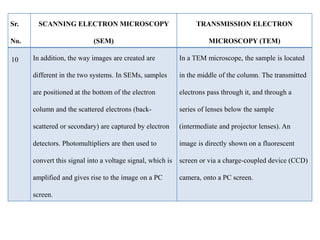
DIFFERENCE BETWEEN SCANNING
ELECTRON MICROSCOPY (SEM) AND
TRANSMISSION ELECTRON
MICROSCOPY (TEM)
Dr. Vrushali Sachinkumar Tambe
Professor (Department of Pharmaceutical Chemistry)
PES Modern College of Pharmacy (for Ladies), Pune,
India
Sr. No. SCANNING ELECTRON
MICROSCOPY (SEM)
TRANSMISSION
ELECTRON MICROSCOPY
(TEM)
1 SEM provides information on the
sample’s surface and its composition.
SEMs use a specific set of coils to scan
the beam in a raster-like pattern and
collect the scattered electrons.
TEM use the transmitted electrons; the
electrons which are passing through the
sample before they are collected. So,
TEM offers invaluable information on the
inner structure of the sample, such as
crystal structure, morphology and stress
state information.
2 SEM resolution is limited to ~0.5 nm. TEM has resolution of even less than 50
pm.
3 If you want to get information on the
surface of your sample, like roughness or
contamination detection, then you should
choose a SEM.
If you would like to know what the
crystal structure of your sample is, or if
you want to look for possible structural
defects or impurities, then using a TEM is
the only way to do so.
Sr.
No.
SCANNING ELECTRON
MICROSCOPY (SEM)
TRANSMISSION ELECTRON
MICROSCOPY (TEM)
4 SEMs provide a 3D image of the
surface of the sample.
TEM images are 2D projections of the sample, which
in some cases makes the interpretation of the results
more difficult for the operator.
5 SEM imaging there is no specific
requirement of sample preparation.
Due to the requirement for transmitted electrons, TEM
samples must be very thin, generally below 150 nm,
and in cases that high-resolution imaging is required,
even below 30 nm.
6 SEM samples require little or no
effort for sample preparation and can
be directly imaged by mounting
them on an aluminum stub.
TEM sample preparation is a quite complex and tedious
procedure that only trained and experienced users can
follow successfully. The samples need to be very thin,
as flat as possible, and the preparation technique should
not induce any artefacts (such as precipitates or
amorphisation) to the sample. Many methods have been
developed, including electro polishing, mechanical
polishing and focused ion beam milling. Dedicated
grids and holders are used to mount the TEM samples.
Sr. No. SCANNING ELECTRON
MICROSCOPY (SEM)
TRANSMISSION ELECTRON
MICROSCOPY (TEM)
7 SEMs usually use acceleration voltages
up to 30 kV.
TEM uses it in the range of 60 – 300 kV.
8 The magnifications for the SEM is
limited up to 1-2 million times.
The magnifications that TEMs is much
higher compared to SEMs. TEM users can
magnify their samples by more than 50
million times,
9 However, the maximum Field of View
(FOV) that SEMs can achieve is far
larger than TEMs, Similarly, the depth of
field of SEM systems are much higher
than in TEM systems.
Users can only use to image a very small
part of their sample.
Sr.
No.
SCANNING ELECTRON MICROSCOPY
(SEM)
TRANSMISSION ELECTRON
MICROSCOPY (TEM)
10 In addition, the way images are created are
different in the two systems. In SEMs, samples
are positioned at the bottom of the electron
column and the scattered electrons (back-
scattered or secondary) are captured by electron
detectors. Photomultipliers are then used to
convert this signal into a voltage signal, which is
amplified and gives rise to the image on a PC
screen.
In a TEM microscope, the sample is located
in the middle of the column. The transmitted
electrons pass through it, and through a
series of lenses below the sample
(intermediate and projector lenses). An
image is directly shown on a fluorescent
screen or via a charge-coupled device (CCD)
camera, onto a PC screen.
Sr. No. SCANNING ELECTRON
MICROSCOPY (SEM)
TRANSMISSION ELECTRON
MICROSCOPY (TEM)
11 Relatively simple to operate Generally, TEMs are more complex to
operate. TEM users require intensive
training before being able to operate them.
Special procedures need to be performed
before every use, with several steps
included that ensure that the electron beam
is perfectly aligned.
12 Relatively simple TEMs may enable much more resolving
power and versatility to the user, but they
are much more expensive and larger than
SEMs and require more effort in order to
acquire and interpret results.

Difference between SEM and TEM

  • 1.
    DIFFERENCE BETWEEN SCANNING ELECTRONMICROSCOPY (SEM) AND TRANSMISSION ELECTRON MICROSCOPY (TEM) Dr. Vrushali Sachinkumar Tambe Professor (Department of Pharmaceutical Chemistry) PES Modern College of Pharmacy (for Ladies), Pune, India
  • 2.
    Sr. No. SCANNINGELECTRON MICROSCOPY (SEM) TRANSMISSION ELECTRON MICROSCOPY (TEM) 1 SEM provides information on the sample’s surface and its composition. SEMs use a specific set of coils to scan the beam in a raster-like pattern and collect the scattered electrons. TEM use the transmitted electrons; the electrons which are passing through the sample before they are collected. So, TEM offers invaluable information on the inner structure of the sample, such as crystal structure, morphology and stress state information. 2 SEM resolution is limited to ~0.5 nm. TEM has resolution of even less than 50 pm. 3 If you want to get information on the surface of your sample, like roughness or contamination detection, then you should choose a SEM. If you would like to know what the crystal structure of your sample is, or if you want to look for possible structural defects or impurities, then using a TEM is the only way to do so.
  • 3.
    Sr. No. SCANNING ELECTRON MICROSCOPY (SEM) TRANSMISSIONELECTRON MICROSCOPY (TEM) 4 SEMs provide a 3D image of the surface of the sample. TEM images are 2D projections of the sample, which in some cases makes the interpretation of the results more difficult for the operator. 5 SEM imaging there is no specific requirement of sample preparation. Due to the requirement for transmitted electrons, TEM samples must be very thin, generally below 150 nm, and in cases that high-resolution imaging is required, even below 30 nm. 6 SEM samples require little or no effort for sample preparation and can be directly imaged by mounting them on an aluminum stub. TEM sample preparation is a quite complex and tedious procedure that only trained and experienced users can follow successfully. The samples need to be very thin, as flat as possible, and the preparation technique should not induce any artefacts (such as precipitates or amorphisation) to the sample. Many methods have been developed, including electro polishing, mechanical polishing and focused ion beam milling. Dedicated grids and holders are used to mount the TEM samples.
  • 4.
    Sr. No. SCANNINGELECTRON MICROSCOPY (SEM) TRANSMISSION ELECTRON MICROSCOPY (TEM) 7 SEMs usually use acceleration voltages up to 30 kV. TEM uses it in the range of 60 – 300 kV. 8 The magnifications for the SEM is limited up to 1-2 million times. The magnifications that TEMs is much higher compared to SEMs. TEM users can magnify their samples by more than 50 million times, 9 However, the maximum Field of View (FOV) that SEMs can achieve is far larger than TEMs, Similarly, the depth of field of SEM systems are much higher than in TEM systems. Users can only use to image a very small part of their sample.
  • 5.
    Sr. No. SCANNING ELECTRON MICROSCOPY (SEM) TRANSMISSIONELECTRON MICROSCOPY (TEM) 10 In addition, the way images are created are different in the two systems. In SEMs, samples are positioned at the bottom of the electron column and the scattered electrons (back- scattered or secondary) are captured by electron detectors. Photomultipliers are then used to convert this signal into a voltage signal, which is amplified and gives rise to the image on a PC screen. In a TEM microscope, the sample is located in the middle of the column. The transmitted electrons pass through it, and through a series of lenses below the sample (intermediate and projector lenses). An image is directly shown on a fluorescent screen or via a charge-coupled device (CCD) camera, onto a PC screen.
  • 6.
    Sr. No. SCANNINGELECTRON MICROSCOPY (SEM) TRANSMISSION ELECTRON MICROSCOPY (TEM) 11 Relatively simple to operate Generally, TEMs are more complex to operate. TEM users require intensive training before being able to operate them. Special procedures need to be performed before every use, with several steps included that ensure that the electron beam is perfectly aligned. 12 Relatively simple TEMs may enable much more resolving power and versatility to the user, but they are much more expensive and larger than SEMs and require more effort in order to acquire and interpret results.