SlideShare a Scribd company logo
Basic Electronics Lab Manual
Sanjay Memorial Polytechnic, Sagar
Basic Electronics Lab Manual
(For First Semester Diploma in Computer Science and Engineering)
Hemanth Y.R
Lecturer, Dept. of E & C
Sanjay Memorial Polytechnic, Sagar
Basic Electronics Lab Manual
Diploma in Computer Science and Engineering)
Sagar
1
2
Basic Electronics Lab Manual
Sanjay Memorial Polytechnic, Sagar
GENERAL OBJECTIVES: No. of Hrs
On completion of the lab course, the student will be able to 96
1 Comprehend the art of Soldering
2 Understand the behavioral characteristics of passive components
GRADED EXERCISES:
SECTION -- A
STUDY EXERCISES
Note: In Study Exercises the student should become familiar with
specification of equipments & components & should draw a neat
diagram of the control panel of equipment & actual appearance in
case of components. Symbols should also be indicated wherever
applicable
1
Familiarization and precautionary measures to be taken while using
the following Equipments –
Analog multimeter, Digital multimeter, Regulated power supply
LCR Meter, Ammeters, Voltmeter and Galvanometer
Ammeters voltmeter and Galvanometer
6
2
Identification of components ----- Passive and Active components
with Symbol
6
3
Colour code--- Calculation of Resistance & Capacitance value by
colour code method
6
4 Measurement of Resistance & Capacitance value by colour codes 6
5
Soldering Practice:
Tool, Bending of Wires, Soldering of Passive and Active components
6
6 Testing of Passive Components 6
7
Familiarization, Study and Application of following Hardware
materials and symbol
FUSES --- Rewirable, Cartridge, High rupturing capacity Fuse
KEYS--- Rectangular Buttons, Spring loaded, Mechanical , Electronic
feather touch
PLUGS AND SOCKETS--- 2 pin, 3 pin, Multiple, Round type
CONNECTORS : IC and relay connector, PCB connector, BNC,
threaded neutral modular
TERMINALS ---Different sizes
CABLES --- twisted pair, co-axial cable, optical cable
CLIPS --- Crocodile , Banana
Crimping tools
6
8
Study the block diagram of UPS & SMPS & state their merits and
demerits
6
Total (Section A) 48
3
Basic Electronics Lab Manual
Sanjay Memorial Polytechnic, Sagar
SECTION -- B
Conduction Exercises:
11 Verification of Ohm's law, 3
12 Verification of Kirchhoff's Current law for D.C Circuits 3
13 Verification of Kirchhoff's Voltage law for D.C Circuits 3
14 Characteristics of junction diode (Forward & Reverse Bias) 6
15 Characteristics of Zener diode (Forward & Reverse bias) 6
16 Inverting amplifier using OP-AMP 3
17 Non-inverting amplifier using OP-AMP 3
18
Half wave rectifier - construction, calculation of ripple factor with
and without shunt capacitor filter
6
19
Full wave bridge rectifier - construction, calculation of ripple factor
with and without shunt capacitor filter
9
Total (Section B) 48
Total 96
SCHEME OF VALUATION
1 Record 5
2 Part A - Study Exercise 25
3
Part B - Write up any One Experiment (Circuit Diagram, Tabular
column, Formula )
20
3 Construction using soldering and Conduction of Experiment 20
4 Result 10
5 Viva-Voce 20
Total 100
4
Basic Electronics Lab Manual
Sanjay Memorial Polytechnic, Sagar
SECTION -- A
Study Exercises
1. Familiarization of meters.
Connecting meters
It is important to connect meters the correct way round:
• The positive terminal of the meter, marked + or coloured red should be connected
nearest to + on the battery or power supply.
• The negative terminal of the meter, marked - or coloured black should be connected
nearest to - on the battery or power supply.
Voltmeters
• Voltmeters measure voltage.
• Voltage is measured in volts, V.
• Voltmeters are connected in parallel across
components.
• Voltmeters have a very high resistance.
Measuring voltage at a point
When testing circuits you often
need to find the voltages at
various points, for example the
voltage at pin 2 of a 555 timer
IC. This can seem confusing -
where should you connect the
second voltmeter lead?
• Connect the black
(negative -) voltmeter
lead to 0V, normally the
negative terminal of the
battery or power
supply.
• Connect the red (positive +) voltmeter lead to the point you where you need to
measure the voltage.
• The black lead can be left permanently connected to 0V while you use the red lead
as a probe to measure voltages at various points.
Connecting a voltmeter in parallel
5
Basic Electronics Lab Manual
Sanjay Memorial Polytechnic, Sagar
• You may wish to use a crocodile clip on the black lead to hold it in place.
Voltage at a point really means the voltage difference between that point and 0V (zero
volts) which is normally the negative terminal of the battery or power supply. Usually 0V will
be labeled on the circuit diagram as a reminder.
Analogue meters take a little power from the circuit under test to operate their pointer. This
may upset the circuit and give an incorrect reading. To avoid this voltmeters should have a
resistance of at least 10 times the circuit resistance (take this to be the highest resistor value
near where the meter is connected).
Most analogue voltmeters used in school science are not suitable for electronics because
their resistance is too low, typically a few k . 100k or more is required for most
electronics circuits.
Ammeters
• Ammeters measure current.
• Current is measured in amps (amperes), A.
1A is quite large, so mA (milliamps) and µA
(microamps) are often used. 1000mA = 1A,
1000µA = 1mA, 1000000µA = 1A.
• Ammeters are connected in series.
To connect in series you must break the circuit
and put the ammeter across the gap, as shown
in the diagram.
• Ammeters have a very low resistance.
The need to break the circuit to connect in series means
that ammeters are difficult to use on soldered circuits. Most testing in electronics is done
with voltmeters which can be easily connected without disturbing circuits.
Galvanometers
Galvanometers are very sensitive meters which are used to
measure tiny currents, usually 1mA or less. They are used to
make all types of analogue meters by adding suitable resistors
as shown in the diagrams below. The photograph shows an
educational 100µA galvanometer for which various multipliers and shunts are available.
Connecting an ammeter in series
6
Basic Electronics Lab Manual
Sanjay Memorial Polytechnic, Sagar
Making a Voltmeter
A galvanometer with a
high resistance
multiplier in series to
make a voltmeter.
Making an Ammeter
A galvanometer with
a low resistance
shunt in parallel to
make an ammeter.
Galvanometer with multiplier and shunt
Maximum meter current 100µA (or 20µA
reverse).
This meter is unusual in allowing small
reverse readings to be shown.
Ohmmeters
An ohmmeter is used to measure resistance in ohms ( ).
Ohmmeters are rarely found as separate meters but all
standard multimeters have an ohmmeter setting.
1 is quite small so k and M are often used.
1k = 1000 , 1M = 1000k = 1000000 .
Multimeters
Multimeters are very useful test
instruments. By operating a multi-
position switch on the meter they can
be quickly and easily set to be a
voltmeter, an ammeter or an
ohmmeter. They have several settings
(called 'ranges') for each type of meter
and the choice of AC or DC.
Some multimeters have additional
features such as transistor testing and
ranges for measuring capacitance and
frequency.
Analogue multimeters consist of a
galvanometer with various resistors which can be switched in as multipliers (voltmeter
ranges) and shunts (ammeter ranges).
Analogue Multimeter Digital Multimeter
Multimeter Photographs © Rapid Electronics
7
Basic Electronics Lab Manual
Sanjay Memorial Polytechnic, Sagar
2. Electronic Components and symbols
1. ACTIVE components increase the power of a signal and must be supplied with the
signal and a source of power.
Examples are bipolar transistors, field effect transistors etc.
The signal is fed into one connection of the active device and the amplified version
taken from another connection.
In a transistor, the signal can be applied to the base connection and the amplified
version taken from the collector.
2. PASSIVE components do not increase the power of a signal.
They often cause power to be lost.
Some can increase the voltage at the expense of current, so overall there is a loss of
power.
Resistors, capacitors, inductors and diodes are examples of passive components.
Some of the active components are
1. Diodes
2. Transistors
3. Integrated circuits
4. Optoelectronic components
Similarly some of the passive components are
1. Resistors
2. Capacitors
3. Inductors
4. Sensors
5. Detectors
6. Antennas
Wires and connections
Component Circuit Symbol Function of Component
Wire
To pass current very easily from one part of
a circuit to another.
Wires joined
A 'blob' should be drawn where wires are
connected (joined), but it is sometimes
omitted. Wires connected at 'crossroads'
should be staggered slightly to form two T-
junctions, as shown on the right.
8
Basic Electronics Lab Manual
Sanjay Memorial Polytechnic, Sagar
Wires not joined
In complex diagrams it is often necessary to
draw wires crossing even though they are
not connected. The simple crossing on the
left is correct but may be misread as a join
where the 'blob' has been forgotten. The
bridge symbol on the right leaves no doubt!
Power Supplies
Component Circuit Symbol Function of Component
Cell
Supplies electrical energy.
The larger terminal (on the left) is positive (+).
A single cell is often called a battery, but strictly
a battery is two or more cells joined together.
Battery
Supplies electrical energy. A battery is more
than one cell.
The larger terminal (on the left) is positive (+).
Solar Cell
Converts light to electrical energy.
The larger terminal (on the left) is positive (+).
DC supply
Supplies electrical energy.
DC = Direct Current, always flowing in one
direction.
AC supply
Supplies electrical energy.
AC = Alternating Current, continually changing
direction.
Fuse
A safety device which will 'blow' (melt) if the
current flowing through it exceeds a specified
value.
Transformer
Two coils of wire linked by an iron core.
Transformers are used to step up (increase) and
step down (decrease) AC voltages. Energy is
transferred between the coils by the magnetic
field in the core. There is no electrical
connection between the coils.
Earth
(Ground)
A connection to earth. For many electronic
circuits this is the 0V (zero volts) of the power
supply, but for mains electricity and some radio
circuits it really means the earth. It is also
known as ground.
9
Basic Electronics Lab Manual
Sanjay Memorial Polytechnic, Sagar
Output Devices: Lamps, Heater, Motor, etc.
Component Circuit Symbol Function of Component
Lamp (lighting)
A transducer which converts electrical energy
to light. This symbol is used for a lamp
providing illumination, for example a car
headlamp or torch bulb.
Lamp (indicator
)
A transducer which converts electrical energy
to light. This symbol is used for a lamp which
is an indicator, for example a warning light on
a car dashboard.
Heater
A transducer which converts electrical energy
to heat.
Motor
A transducer which converts electrical energy
to kinetic energy (motion).
Bell
A transducer which converts electrical energy
to sound.
Buzzer
A transducer which converts electrical energy
to sound.
Inductor
(Coil, Solenoid)
A coil of wire which creates a magnetic field
when current passes through it. It may have
an iron core inside the coil. It can be used as a
transducer converting electrical energy to
mechanical energy by pulling on something.
Switches
Component Circuit Symbol Function of Component
Push Switch
(push-to-
make)
A push switch allows current to flow only
when the button is pressed. This is the
switch used to operate a doorbell.
Push-to-Break
Switch
This type of push switch is normally closed
(on), it is open (off) only when the button is
pressed.
On-Off Switch
(SPST)
SPST = Single Pole, Single Throw.
An on-off switch allows current to flow only
when it is in the closed (on) position.
10
Basic Electronics Lab Manual
Sanjay Memorial Polytechnic, Sagar
2-way Switch
(SPDT)
SPDT = Single Pole, Double Throw.
A 2-way changeover switch directs the flow
of current to one of two routes according
to its position. Some SPDT switches have a
central off position and are described as
'on-off-on'.
Dual On-Off
Switch
(DPST)
DPST = Double Pole, Single Throw.
A dual on-off switch which is often used to
switch mains electricity because it can
isolate both the live and neutral
connections.
Reversing
Switch
(DPDT)
DPDT = Double Pole, Double Throw.
This switch can be wired up as a reversing
switch for a motor. Some DPDT switches
have a central off position.
Relay
An electrically operated switch, for
example a 9V battery circuit connected to
the coil can switch a 230V AC mains circuit.
NO = Normally Open, COM = Common,
NC = Normally Closed.
Resistors
Component Circuit Symbol Function of Component
Resistor
A resistor restricts the flow of current, for
example to limit the current passing through
an LED. A resistor is used with a capacitor in
a timing circuit.
Some publications use the old resistor
symbol:
Variable Resistor
(Rheostat)
This type of variable resistor with 2 contacts
(a rheostat) is usually used to control
current. Examples include: adjusting lamp
brightness, adjusting motor speed, and
adjusting the rate of flow of charge into a
capacitor in a timing circuit.
Variable Resistor
(Potentiometer)
This type of variable resistor with 3 contacts
(a potentiometer) is usually used to control
voltage. It can be used like this as a
transducer converting position (angle of the
control spindle) to an electrical signal.
11
Basic Electronics Lab Manual
Sanjay Memorial Polytechnic, Sagar
Variable Resistor
(Preset)
This type of variable resistor (a preset) is
operated with a small screwdriver or similar
tool. It is designed to be set when the circuit
is made and then left without further
adjustment. Presets are cheaper than
normal variable resistors so they are often
used in projects to reduce the cost.
Capacitors
Component Circuit Symbol Function of Component
Capacitor
A capacitor stores electric charge. A
capacitor is used with a resistor in a timing
circuit. It can also be used as a filter, to
block DC signals but pass AC signals.
Capacitor,
polarised
A capacitor stores electric charge. This
type must be connected the correct way
round. A capacitor is used with a resistor
in a timing circuit. It can also be used as a
filter, to block DC signals but pass AC
signals.
Variable Capacitor
A variable capacitor is used in a radio
tuner.
Trimmer
Capacitor
This type of variable capacitor (a trimmer)
is operated with a small screwdriver or
similar tool. It is designed to be set when
the circuit is made and then left without
further adjustment.
Diodes
Component Circuit Symbol Function of Component
Diode
A device which only allows current to
flow in one direction.
LED
Light Emitting Diode
A transducer which converts electrical
energy to light.
Zener Diode
A special diode which is used to maintain
a fixed voltage across its terminals.
Photodiode A light-sensitive diode.
12
Basic Electronics Lab Manual
Sanjay Memorial Polytechnic, Sagar
Transistors
Component Circuit Symbol Function of Component
Transistor NPN
A transistor amplifies current. It can be used with other
components to make an amplifier or switching circuit.
Transistor PNP
A transistor amplifies current. It can be used with other
components to make an amplifier or switching circuit.
Phototransistor A light-sensitive transistor.
Audio and Radio Devices
Component Circuit Symbol Function of Component
Microphone
A transducer which converts sound to electrical
energy.
Earphone
A transducer which converts electrical energy to
sound.
Loudspeaker
A transducer which converts electrical energy to
sound.
Piezo Transducer
A transducer which converts electrical energy to
sound.
Amplifier
(general symbol)
An amplifier circuit with one input. Really it is a
block diagram symbol because it represents a
circuit rather than just one component.
13
Basic Electronics Lab Manual
Sanjay Memorial Polytechnic, Sagar
Aerial
(Antenna)
A device which is designed to receive or transmit
radio signals. It is also known as an antenna.
Meters and Oscilloscope
Component Circuit Symbol Function of Component
Voltmeter
A voltmeter is used to measure voltage.
The proper name for voltage is 'potential
difference', but most people prefer to say
voltage!
Ammeter An ammeter is used to measure current.
Galvanometer
A galvanometer is a very sensitive meter which
is used to measure tiny currents, usually 1mA
or less.
Ohmmeter
An ohmmeter is used to measure resistance.
Most multimeters have an ohmmeter setting.
Oscilloscope
An oscilloscope is used to display the shape of
electrical signals and it can be used to measure
their voltage and time period.
Sensors (input devices)
Component Circuit Symbol Function of Component
LDR
A transducer which converts brightness (light)
to resistance (an electrical property).
LDR = Light Dependent Resistor
Thermistor
A transducer which converts temperature (heat)
to resistance (an electrical property).
14
Basic Electronics Lab Manual
Sanjay Memorial Polytechnic, Sagar
3. Colour code
Resistor values - the resistor colour code
Resistance is measured in ohms, the symbol for ohm is an omega .
1 is quite small so resistor values are often given in k and M .
1 k = 1000 1 M = 1000000 .
Resistor values are normally shown using coloured bands.
Each colour represents a number as shown in the table.
Most resistors have 4 bands:
• The first band gives the first digit.
• The second band gives the second digit.
• The third band indicates the number of zeros.
• The fourth band is used to shows the tolerance (precision) of the
resistor, this may be ignored for almost all circuits but further
details are given below.
This resistor has red (2), violet (7), yellow (4 zeros) and gold bands.
So its value is 270000 = 270 k .
On circuit diagrams the is usually omitted and the value is written 270K.
Small value resistors (less than 10 ohm)
The standard colour code cannot show values of less than 10 . To show these small values
two special colours are used for the third band: gold which means × 0.1 and silver which
means × 0.01. The first and second bands represent the digits as normal.
For example:
red, violet, gold bands represent 27 × 0.1 = 2.7
green, blue, silver bands represent 56 × 0.01 = 0.56
Tolerance of resistors (fourth band of colour code)
The tolerance of a resistor is shown by the fourth band of the colour code. Tolerance is the
precision of the resistor and it is given as a percentage. For example a 390 resistor with a
tolerance of ±10% will have a value within 10% of 390 , between 390 - 39 = 351 and 390
+ 39 = 429 (39 is 10% of 390).
The Resistor
Colour Code
Colour Number
Black 0
Brown 1
Red 2
Orange 3
Yellow 4
Green 5
Blue 6
Violet 7
Grey 8
White 9
15
Basic Electronics Lab Manual
Sanjay Memorial Polytechnic, Sagar
A special colour code is used for the fourth band tolerance:
silver ±10%, gold ±5%, red ±2%, brown ±1%.
If no fourth band is shown the tolerance is ±20%.
Tolerance may be ignored for almost all circuits because precise resistor values are rarely
required.
Resistor shorthand
Resistor values are often written on circuit diagrams using a code system which avoids using
a decimal point because it is easy to miss the small dot. Instead the letters R, K and M are
used in place of the decimal point. To read the code: replace the letter with a decimal point,
then multiply the value by 1000 if the letter was K, or 1000000 if the letter was M. The letter
R means multiply by 1.
For example:
560R means 560
2K7 means 2.7 k = 2700
39K means 39 k
1M0 means 1.0 M = 1000 k
16
Basic Electronics Lab Manual
Sanjay Memorial Polytechnic, Sagar
4. Soldering
What is solder?
Traditional solder is an alloy (mixture) of tin and lead, typically 60% tin and 40% lead. It
melts at a temperature of about 200°C.
Modern lead-free solder is an alloy of tin with other metals including copper and silver. It
melts at a temperature of about 220°C.
Coating a surface with solder is called 'tinning' because of the tin content of solder.
Desoldering
At some stage you will probably need to desolder a joint to remove or re-position a wire or
component. There are two ways to
remove the solder:
1. With a desoldering pump (solder
sucker)
• Set the pump by pushing the
spring-loaded plunger down until
it locks.
• Apply both the pump nozzle and
the tip of your soldering iron to
the joint.
• Wait a second or two for the
solder to melt.
• Then press the button on the
pump to release the plunger and
suck the molten solder into the
tool.
• Repeat if necessary to remove as much solder as possible.
• The pump will need emptying occasionally by unscrewing the nozzle.
How to Solder
First a few safety precautions:
• Never touch the element or tip of the soldering iron.
They are very hot (about 400°C) and will give you a nasty burn.
• Take great care to avoid touching the mains flex with the tip of the iron.
The iron should have a heatproof flex for extra protection. An ordinary plastic flex
will melt immediately if touched by a hot iron and there is a serious risk of burns and
electric shock.
• Always return the soldering iron to its stand when not in use.
Never put it down on your workbench, even for a moment!
Using a desoldering pump (solder sucker)
17
Basic Electronics Lab Manual
Sanjay Memorial Polytechnic, Sagar
• Work in a well-ventilated area.
The smoke formed as you melt solder is mostly from the flux and quite irritating.
Avoid breathing it by keeping you head to the side of, not above, your work.
• Wash your hands after using solder.
Traditional solder contains lead which is a poisonous metal.
Preparing the soldering iron:
• Place the soldering iron in its stand and plug in.
The iron will take a few minutes to reach its operating temperature of about 400°C.
• Dampen the sponge in the stand.
The best way to do this is to lift it out the stand and hold it under a cold tap for a
moment, then squeeze to remove excess water. It should be damp, not dripping wet.
• Wait a few minutes for the soldering iron to warm up.
You can check if it is ready by trying to melt a little solder on the tip.
• Wipe the tip of the iron on the damp sponge.
This will clean the tip.
• Melt a little solder on the tip of the iron.
This is called 'tinning' and it will help the heat to flow from the iron's tip to the joint.
It only needs to be done when you plug in the iron, and occasionally while soldering
if you need to wipe the tip clean on the sponge.
You are now ready to start
soldering:
• Hold the soldering iron like
a pen, near the base of the
handle.
Imagine you are going to
write your name!
Remember to never touch
the hot element or tip.
• Touch the soldering iron
onto the joint to be made.
Make sure it touches both
the component lead and the track. Hold the tip there for a few seconds and...
• Feed a little solder onto the joint.
It should flow smoothly onto the lead and track to form a volcano shape as shown in
the diagram. Apply the solder to the joint, not the iron.
• Remove the solder, then the iron, while keeping the joint still.
Allow the joint a few seconds to cool before you move the circuit board.
• Inspect the joint closely.
It should look shiny and have a 'volcano' shape. If not, you will need to reheat it and
feed in a little more solder. This time ensure that both the lead and track are heated
fully before applying solder.
18
Basic Electronics Lab Manual
Sanjay Memorial Polytechnic, Sagar
SECTION -- B
Conduction Exercises
Experiment No. 1
Verification of Ohm's law
Aim of the Experiment:
To study the dependence of current (I) on the potential difference (V) across a
resistor and determine its resistance. Also plot a graph between V and I.
In this lab, you will verify Ohms Law for different values of voltage and
resistances. You will measure the true resistance of each resistor and the voltage applied to
each resistor. You will then calculate the predicted current through each resistor. Finally,
you will measure the actual current through each resistor to verify (or disprove!) Ohm’s
Law.
Equipments & Components Required:
1. Rheostat or Decade resistance box.
2. Regulated power supply.
3. Connecting wires.
4. Multimeter.
Theory:
The Ohm’s law states that the direct current flowing in a conductor is directly
proportional to the potential difference between its ends. It is usually formulated as V = IR,
where V is the potential difference, or voltage, I is the current, and R is the resistance of the
conductor.
Basic Electronics Lab Manual
Sanjay Memorial Polytechnic, Sagar
Consider the circuit shown below
The resistance of that circuit would be given by R=V/I
The current flowing through the circuit would be given by
The voltage would be given by I x R
Following figure shows graph of Voltage V/s Current
Experiment:
Circuit Diagram:
Sanjay Memorial Polytechnic, Sagar
Consider the circuit shown below
The resistance of that circuit would be given by R=V/I = 24/2 = 12 ohms
The current flowing through the circuit would be given by V/IR 24/12 = 2amps
The voltage would be given by I x R = 2 x 12 = 24 volts
Following figure shows graph of Voltage V/s Current
19
24/2 = 12 ohms
V/IR 24/12 = 2amps
20
Basic Electronics Lab Manual
Sanjay Memorial Polytechnic, Sagar
Data Table:
Resistance R = 1 KΩ Resistance R = 2 KΩ
Trial
No.
Voltage V
Applied in
Volts
Current I
Thro’ R
in mili
amps
Current I
By Ohm’s
Law
I=V/R
Trial
No.
Voltage V
Applied in
Volts
Current I
Thro’ R
in mili
amps
Current I
By Ohm’s
Law
I=V/R
1 1 1 1
2 2 2 2
3 3 3 3
4 4 4 4
5 5 5 5
6 6 6 6
7 7 7 7
8 8 8 8
9 9 9 9
10 10 10 10
Calculations Here ↓:
21
Basic Electronics Lab Manual
Sanjay Memorial Polytechnic, Sagar
Procedure:
1. Before doing the connection, check all the components and equipments.
2. Make the connection as shown in the circuit diagram.
3. Keep value of Rheostat or DRB to 1 KΩ and start first set of ten trials.
4. Vary voltage applied across R from 1V to 10V and record corresponding values of
current from the ammeter.
5. Also calculate theoretical values of current using ohm’s law and record in the
data table.
6. Observe the difference between theoretical and practical values of current.
7. Repeat from step 3 by keeping value of Rheostat or DRB to 2 K Ohm.
Results:
Basic Electronics Lab Manual
Sanjay Memorial Polytechnic, Sagar
Verification of Kirch
Aim of the Experiment:
To verify Kirchhoff’s current law.
Equipments & Components Required:
1. Two fixed value resistors.
2. Regulated power supply.
3. Connecting wires.
4. Ammeter or Multimeter.
Theory:
Kirchhoff's first law, Kirchhoff's point rule
states that at any node (junction) in an electrical circuit, the sum of currents flowing into
that node is equal to the sum of currents flowing out of that
currents in a network of conductors meeting at a point is zero.
The current entering any junction is equal to the current leaving that junction.
i2 + i3 = i1 + i4
Experiment No. 2
Verification of Kirchhoff's Current law for D.C Circuits
To verify Kirchhoff’s current law.
Equipments & Components Required:
Two fixed value resistors.
Regulated power supply.
Multimeter.
Kirchhoff's point rule, or Kirchhoff's junction rule
at any node (junction) in an electrical circuit, the sum of currents flowing into
that node is equal to the sum of currents flowing out of that node or the algebraic sum of
currents in a network of conductors meeting at a point is zero.
The current entering any junction is equal to the current leaving that junction.
22
off's Current law for D.C Circuits
Kirchhoff's junction rule (or nodal rule)
at any node (junction) in an electrical circuit, the sum of currents flowing into
node or the algebraic sum of
The current entering any junction is equal to the current leaving that junction.
23
Basic Electronics Lab Manual
Sanjay Memorial Polytechnic, Sagar
Experiment:
Circuit Diagram:
Current Equations:
Equivalent Resistance REQU = (R1*R2) / (R1+R2)
Total Current I = V/ REQU
Current Thro’ R1 is I1 = V/ R1
Current Thro’ R2 is I2= V/ R2
Data Table:
Trial
No.
Voltage V
Applied in
Volts
Theoretical Values Practical Values
Current
I in mili
amps
Current
I1
in mili
amps
Current
I2
in mili
amps
Current
I in mili
amps
Current
I1
in mili
amps
Current
I2
in mili
amps
1 0
2 5
3 10
4 15
5 20
6 25
7 30
V
30V
R1
1.0kohm
R2
2.0kohm
0.045 A
+ -
0.030 A
+
-
0.015 A
+
-
24
Basic Electronics Lab Manual
Sanjay Memorial Polytechnic, Sagar
Calculations Here ↓:
Procedure:
1. Before doing the connection, check all the components and equipments.
2. Make the connection as shown in the circuit diagram.
3. Take two fixed value resistors R1 and R2.
4. Vary voltage applied from 0V to 30V in steps of 5V and record corresponding
values of currents I, I1 and I2 from corresponding ammeters.
5. Also calculate theoretical values of current using equations given above and
record in the data table.
6. Observe the difference between theoretical and practical values of currents.
Results:
25
Basic Electronics Lab Manual
Sanjay Memorial Polytechnic, Sagar
Experiment No. 3
Verification of Kirchhoff's Voltage law for D.C Circuits
Aim of the Experiment:
To verify Kirchhoff’s voltage law.
Equipments & Components Required:
1. Two fixed value resistors.
2. Regulated power supply.
3. Connecting wires.
4. Ammeter or Multimeter.
Theory:
Kirchhoff's second law, Kirchhoff's loop (or mesh) rule states that the algebraic sum
of the voltage (potential) differences in any loop must equal zero.
If we consider a closed loop, conventionally if we consider all the voltage gains along
the loop are positive then all the voltage drops along the loop should be considered as
negative. The summation of all these voltages in a closed loop is equal to zero.
Suppose n numbers of back to back connected elements form a closed loop. Among
these circuit element m number elements are voltage source and n – m number of elements
are resistors then,
The voltages of sources are V1, V2, V3,………………. Vm and voltage drops across the
resistors respectively, Vm + 1, Vm + 2, Vm + 3,………………… Vn.
26
Basic Electronics Lab Manual
Sanjay Memorial Polytechnic, Sagar
As it said that the voltage gain conventionally considered as positive, and voltage
drops are considered as negative, the voltages along the closed loop are
+ V1, + V2, + V3,………………. + Vm, − Vm + 1, − Vm + 2, − Vm + 3,…………………− Vn.
Now according to Kirchhoff Voltage law the summation of all these voltages results to zero.
That means, V1 + V2 + V3 + …………. + Vm − Vm + 1 − Vm + 2 − Vm + 3 + ……………− Vn = 0
So accordingly Kirchhoff Second Law, ∑V = 0
Experiment:
Circuit Diagram:
Current and Voltage Equations:
Equivalent Resistance REQU = R1+R2
Total Current I = V/ REQU
Voltage across R1 is V1 = I * R1
Voltage across R2 is V2 = I * R2
V
30V
R1
1.0kohm
R2
2.0kohm
0.010 A
+ -
10.007 V
+
-
19.993 V
+
-
27
Basic Electronics Lab Manual
Sanjay Memorial Polytechnic, Sagar
Data Table:
Trial
No.
Voltage V
Applied in
Volts
Theoretical Values Practical Values
Current
I in mili
amps
Voltage
V1 in
Volts
Voltage
V2 in
Volts
Current
I in mili
amps
Voltage
V1 in
Volts
Voltage
V2 in
Volts
1 0
2 5
3 10
4 15
5 20
6 25
7 30
Calculations Here ↓:
28
Basic Electronics Lab Manual
Sanjay Memorial Polytechnic, Sagar
Procedure:
1. Before doing the connection, check all the components and equipments.
2. Make the connection as shown in the circuit diagram.
3. Take two fixed value resistors R1 and R2.
4. Vary voltage applied from 0V to 30V in steps of 5V and record corresponding
values of currents I, V1 and V2 from corresponding meters.
5. Also calculate theoretical values of current I, Voltages V1 and V2 using equations
given above and record in the data table.
6. Observe the difference between theoretical and practical values.
Results:
Basic Electronics Lab Manual
Sanjay Memorial Polytechnic, Sagar
Characteristics of junction diode (Forward & Reverse Bias)
Aim of the Experiment:
To study characteristics of junction diode in both forward and reverse
Equipments & Components Required:
1. Resistors - 1K
2. Diode – BY127, 1N4001, …, 1N4007
3. Regulated power supply.
4. Connecting wires.
5. Ammeter and Multimeter.
Theory:
A diode is a two-terminal
low (ideally zero) resistance
resistance in the other.
A p–n junction diode is made of a crystal of
it to create a region on one side that contains negative
type semiconductor, and a region on the other side that contains positive charge carriers
(holes), called p-type semiconductor
attached together, a momentary flow of electrons occur from n to p side resulti
region where no charge carriers are present. It is called Depletion region due to the absence
of charge carriers (electrons and holes in this case). The diode's terminals are attached to
each of these regions. The boundary between these two r
where the action of the diode takes place. The crystal allows electrons to flow from the N
type side (called the cathode
direction.
The symbol used for a semiconductor diode in a
diode. There are alternate symbols for some types of diodes, though the differences are
minor.
Diode LED
Zener Diode Tunnel Diode
Sanjay Memorial Polytechnic, Sagar
Experiment No. 4
Characteristics of junction diode (Forward & Reverse Bias)
To study characteristics of junction diode in both forward and reverse
Equipments & Components Required:
1KΩ
BY127, 1N4001, …, 1N4007
Regulated power supply.
Connecting wires.
Multimeter.
terminal electronic component with asymmetric
resistance to current flow in one direction, and high (ideally
n junction diode is made of a crystal of semiconductor. Impurities are added to
it to create a region on one side that contains negative charge carriers
, and a region on the other side that contains positive charge carriers
type semiconductor. When two materials i.e. n-
attached together, a momentary flow of electrons occur from n to p side resulti
region where no charge carriers are present. It is called Depletion region due to the absence
of charge carriers (electrons and holes in this case). The diode's terminals are attached to
each of these regions. The boundary between these two regions, called a
where the action of the diode takes place. The crystal allows electrons to flow from the N
cathode) to the P-type side (called the anode), but not in the opposite
The symbol used for a semiconductor diode in a circuit diagram
diode. There are alternate symbols for some types of diodes, though the differences are
Photo Diode Schottky diode
Tunnel Diode Varicap
29
Characteristics of junction diode (Forward & Reverse Bias)
To study characteristics of junction diode in both forward and reverse bias condition.
with asymmetric conductance, it has
nt flow in one direction, and high (ideally infinite)
. Impurities are added to
charge carriers (electrons), called n-
, and a region on the other side that contains positive charge carriers
type and p-type are
attached together, a momentary flow of electrons occur from n to p side resulting in a third
region where no charge carriers are present. It is called Depletion region due to the absence
of charge carriers (electrons and holes in this case). The diode's terminals are attached to
egions, called a p–n junction, is
where the action of the diode takes place. The crystal allows electrons to flow from the N-
), but not in the opposite
circuit diagram specifies the type of
diode. There are alternate symbols for some types of diodes, though the differences are
Schottky diode
30
Basic Electronics Lab Manual
Sanjay Memorial Polytechnic, Sagar
Junction Diode Symbol and Static I-V Characteristics.
Forward Biased Junction Diode
When a diode is connected in a Forward Bias condition, a negative voltage is applied
to the N-type material and a positive voltage is applied to the P-type material. If this
external voltage becomes greater than the value of the potential barrier, approx. 0.7 volts
for silicon and 0.3 volts for germanium, the potential barriers opposition will be overcome
and current will start to flow.
This is because the negative voltage pushes or repels electrons towards the junction
giving them the energy to cross over and combine with the holes being pushed in the
opposite direction towards the junction by the positive voltage. This results in a
characteristics curve of zero current flowing up to this voltage point, called the "knee" on
the static curves and then a high current flow through the diode with little increase in the
external voltage as shown below.
Forward Characteristics Curve for a Junction Diode
31
Basic Electronics Lab Manual
Sanjay Memorial Polytechnic, Sagar
The application of a forward biasing voltage on the junction diode results in the
depletion layer becoming very thin and narrow which represents a low impedance path
through the junction thereby allowing high currents to flow. The point at which this sudden
increase in current takes place is represented on the static I-V characteristics curve above as
the "knee" point.
Forward Biased Junction Diode showing a Reduction in the Depletion Layer
This condition represents the low resistance path through the PN junction allowing
very large currents to flow through the diode with only a small increase in bias voltage. The
actual potential difference across the junction or diode is kept constant by the action of the
depletion layer at approximately 0.3v for germanium and approximately 0.7v for silicon
junction diodes.
Since the diode can conduct "infinite" current above this knee point as it effectively
becomes a short circuit, therefore resistors are used in series with the diode to limit its
current flow. Exceeding its maximum forward current specification causes the device to
dissipate more power in the form of heat than it was designed for resulting in a very quick
failure of the device.
Reverse Biased Junction Diode
When a diode is connected in a Reverse Bias condition, a positive voltage is applied
to the N-type material and a negative voltage is applied to the P-type material. The positive
voltage applied to the N-type material attracts electrons towards the positive electrode and
away from the junction, while the holes in the P-type end are also attracted away from the
junction towards the negative electrode.
The net result is that the depletion layer grows wider due to a lack of electrons and
holes and presents a high impedance path, almost an insulator. The result is that a high
potential barrier is created thus preventing current from flowing through the semiconductor
material.
32
Basic Electronics Lab Manual
Sanjay Memorial Polytechnic, Sagar
Reverse Biased Junction Diode showing an Increase in the Depletion Layer
This condition represents a high resistance value to the PN junction and practically
zero current flows through the junction diode with an increase in bias voltage. However, a
very small leakage current does flow through the junction which can be measured in
microamperes, (μA). One final point, if the reverse bias voltage Vr applied to the diode is
increased to a sufficiently high enough value, it will cause the PN junction to overheat and
fail due to the avalanche effect around the junction. This may cause the diode to become
shorted and will result in the flow of maximum circuit current, and this shown as a step
downward slope in the reverse static characteristics curve below.
Reverse Characteristics Curve for a Junction Diode
Sometimes this avalanche effect has practical applications in voltage stabilising
circuits where a series limiting resistor is used with the diode to limit this reverse
breakdown current to a preset maximum value thereby producing a fixed voltage output
across the diode. These types of diodes are commonly known as Zener Diodes and are
discussed in a later tutorial.
33
Basic Electronics Lab Manual
Sanjay Memorial Polytechnic, Sagar
Experiment:
Circuit Diagram:
Forward Biased Junction Diode
Data Table:
Trial
No.
Forward
Voltage Vd
In Volts
Forward
Current Id in
mili amps
1 0.1
2 0.2
3 0.3
4 0.4
5 0.5
6 0.6
7 0.7
8 0.8
9 0.9
10 1.0
V1
30V
R1
1.0kohm
0.029 A
+ -
0.668 V
+
-
D1
1N4001GP
34
Basic Electronics Lab Manual
Sanjay Memorial Polytechnic, Sagar
Reverse Biased Junction Diode
Data Table:
Trial
No.
Reverse Voltage
Vr
In Volts
Reverse Current
Ir in micro amps
1 2
2 4
3 6
4 8
5 10
6 12
7 14
8 16
9 18
10 20
V1
30V
R1
1.0kohm
0.028m A
+ -
29.969 V
+
-
D1
1N4001GP
35
Basic Electronics Lab Manual
Sanjay Memorial Polytechnic, Sagar
Procedure:
1. Before doing the connection, check all the components and equipments.
2. Make the connection as shown in the circuit diagram.
3. Vary the applied voltage in both forward and reverse bias as given in the data
table.
4. Record forward and reverse currents in both forward and reverse conditions.
5. Plot a graph for both forward and reverse bias conditions by taking voltage along
the X-axis and current along Y-axis
Results:
36
Basic Electronics Lab Manual
Sanjay Memorial Polytechnic, Sagar
Experiment No. 5
Characteristics of zener diode (Forward & Reverse Bias)
Aim of the Experiment:
To study characteristics of zener diode in both forward and reverse bias condition.
Equipments & Components Required:
1. Resistors - 1KΩ
2. Zener Diode
3. Regulated power supply.
4. Connecting wires.
5. Ammeter and Multimeter.
Theory:
A Zener diode is a diode which allows current to flow in the forward direction in the
same manner as an ideal diode, but will also permit it to flow in the reverse direction when
the voltage is above a certain value known as the breakdown voltage, "zener knee voltage",
"zener voltage" or "avalanche point".
A conventional solid-state diode will allow significant current if it is reverse-biased
above its reverse breakdown voltage. When the reverse bias breakdown voltage is
exceeded, a conventional diode is subject to high current due to avalanche breakdown.
Unless this current is limited by circuitry, the diode will be permanently damaged due to
overheating. A zener diode exhibits almost the same properties, except the device is
specially designed so as to have a reduced breakdown voltage, the so-called zener voltage.
By contrast with the conventional device, a reverse-biased zener diode will exhibit a
controlled breakdown and allow the current to keep the voltage across the zener diode
close to the zener breakdown voltage. For example, a diode with a zener breakdown voltage
of 3.2 V will exhibit a voltage drop of very nearly 3.2 V across a wide range of reverse
currents. The zener diode is therefore ideal for applications such as the generation of a
reference voltage (e.g. for an amplifier stage), or as a voltage stabilizer for low-current
applications.
Example: Circuit
symbol:
a = anode, k = cathode
Zener diodes are used to maintain a fixed voltage. They are
designed to 'breakdown' in a reliable and non-destructive
way so that they can be used in reverse to maintain a fixed
voltage across their terminals. The diagram shows how
they are connected, with a resistor in series to limit the
current.
37
Basic Electronics Lab Manual
Sanjay Memorial Polytechnic, Sagar
Zener diodes can be distinguished from ordinary diodes by their code and breakdown
voltage which are printed on them. Zener diode codes begin BZX... or BZY... Their
breakdown voltage is printed with V in place of a decimal point, so 4V7 means 4.7V for
example.
Zener diodes are rated by their breakdown voltage and maximum power:
• The minimum voltage available is 2.4V.
• Power ratings of 400mW and 1.3W are common.
Zener Diode Symbol and Static I-V Characteristics.
38
Basic Electronics Lab Manual
Sanjay Memorial Polytechnic, Sagar
Experiment:
Circuit Diagram:
Forward Biased Zener Diode
Data Table:
Trial
No.
Forward
Voltage Vd
In Volts
Forward
Current Id in
mili amps
1 0.1
2 0.2
3 0.3
4 0.4
5 0.5
6 0.6
7 0.7
8 0.8
9 0.9
10 1.0
V1
30V
R1
1.0kohm
0.029 A
+ -
0.627 V
+
-
D1
RD4.7
39
Basic Electronics Lab Manual
Sanjay Memorial Polytechnic, Sagar
Reverse Biased Zener Diode
Data Table:
Trial
No.
Reverse Voltage
Vr
In Volts
Reverse Current
Ir in micro amps
1 2
2 4
3 6
4 8
5 10
6 12
7 14
8 16
9 18
10 20
V1
10V
R1
1.0kohm
5.034m A
+ -
4.965 V
+
-
D1
RD4.7
40
Basic Electronics Lab Manual
Sanjay Memorial Polytechnic, Sagar
Procedure:
1. Before doing the connection, check all the components and equipments.
2. Make the connection as shown in the circuit diagram.
3. Vary the diode voltage in both forward and reverse bias as given in the data
table.
4. Record forward and reverse currents in both forward and reverse conditions.
5. Plot a graph for both forward and reverse bias conditions by taking voltage along
the X-axis and current along Y-axis
Results:
Basic Electronics Lab Manual
Sanjay Memorial Polytechnic, Sagar
Inverting amplifier using OP
Aim of the Experiment:
To study OP-AMP as an inverting amplifier
Equipments & Components Required:
1. Resistors - 1K
2. OP-AMP - µA741
3. Regulated power supply.
4. Signal Generator
5. Connecting wires.
6. CRO.
Theory:
An operational amplifier (op
amplifier with a differential input
an op-amp produces an output potential (relative to circuit ground) that is typically
hundreds of thousands of times larger than the potential difference between its input
terminals.
Circuit notation
Circuit diagram symbol for an
The circuit symbol for an op
• V+: non-inverting input
• V−: inverting input
• Vout: output
• VS+: positive power supply
• VS−: negative power supply
Sanjay Memorial Polytechnic, Sagar
Experiment No. 6
Inverting amplifier using OP-AMP
AMP as an inverting amplifier.
Equipments & Components Required:
1KΩ & 10KΩ
µA741
Regulated power supply.
Signal Generator
Connecting wires.
An operational amplifier (op-amp) is a DC-coupled high-gain
differential input and, usually, a single-ended output. In this
amp produces an output potential (relative to circuit ground) that is typically
hundreds of thousands of times larger than the potential difference between its input
Circuit diagram symbol for an op-amp
The circuit symbol for an op-amp is shown to the right, where:
inverting input
: inverting input
: output
: positive power supply
: negative power supply
41
gain electronic voltage
ended output. In this configuration,
amp produces an output potential (relative to circuit ground) that is typically
hundreds of thousands of times larger than the potential difference between its input
Basic Electronics Lab Manual
Sanjay Memorial Polytechnic, Sagar
Operation
An op-amp without negative feedback (a comparator)
The amplifier's differential inputs consist of a
op-amp amplifies only the difference in voltage between the two, which is called the
differential input voltage. The output voltage of the op
Where V+ is the voltage at the non
inverting terminal and A
loop" refers to the absence of a feedback loop from the output to the input).
The magnitude of AOL is typically very large
op-amps—and therefore even a quite small difference between V+ and V
amplifier output nearly to the supply voltage. Situations in which the output voltage
is equal to or greater than the supply voltage are referred to as saturation of the
amplifier. The magnitude of AOL is not well controlled by the manufacturing process,
and so it is impractical to use an operational amplifier as a stand
amplifier. Without negative feedback
inverting input is held at ground (0 V) directly or by a resistor, and the input voltage
Vin applied to the non-
positive; if Vin is negative, the output will be maximum negative. Since there is no
feedback from the output to either input, this is an
comparator.
An op-amp with negative feedback (a non
amp without negative feedback (a comparator)
The amplifier's differential inputs consist of a V+ input and a V− input, and ideally the
amp amplifies only the difference in voltage between the two, which is called the
. The output voltage of the op-amp is given by the equa
is the voltage at the non-inverting terminal, V− is the voltage at the
AOL is the open-loop gain of the amplifier (the term "open
loop" refers to the absence of a feedback loop from the output to the input).
The magnitude of AOL is typically very large—100,000 or more for integrated circuit
and therefore even a quite small difference between V+ and V
amplifier output nearly to the supply voltage. Situations in which the output voltage
ual to or greater than the supply voltage are referred to as saturation of the
amplifier. The magnitude of AOL is not well controlled by the manufacturing process,
and so it is impractical to use an operational amplifier as a stand-alone
negative feedback, an op-amp acts as a comparator
inverting input is held at ground (0 V) directly or by a resistor, and the input voltage
-inverting input is positive, the output will be maximum
tive; if Vin is negative, the output will be maximum negative. Since there is no
feedback from the output to either input, this is an open loop circuit acti
amp with negative feedback (a non-inverting amplifier)
42
input, and ideally the
amp amplifies only the difference in voltage between the two, which is called the
amp is given by the equation:
is the voltage at the
gain of the amplifier (the term "open-
loop" refers to the absence of a feedback loop from the output to the input).
100,000 or more for integrated circuit
and therefore even a quite small difference between V+ and V− drives the
amplifier output nearly to the supply voltage. Situations in which the output voltage
ual to or greater than the supply voltage are referred to as saturation of the
amplifier. The magnitude of AOL is not well controlled by the manufacturing process,
alone differential
comparator. If the
inverting input is held at ground (0 V) directly or by a resistor, and the input voltage
inverting input is positive, the output will be maximum
tive; if Vin is negative, the output will be maximum negative. Since there is no
circuit acting as a
inverting amplifier)
Basic Electronics Lab Manual
Sanjay Memorial Polytechnic, Sagar
If predictable operation is desired, negative feedback is used, by applying a portion
of the output voltage to the inverting input. The
reduces the gain of the amplifier. When negative feedback is used, the circuit's
overall gain and response becomes determined mostly by the feedback network
rather than by the op
For example, in a non
negative feedback via the voltage divider Rf, Rg reduces the gain. Equilibrium will be
established when Vout is just sufficient to reach around and "pull" the inverting
input to the same voltage as Vin. The voltage gain of the entire circuit is determined
by 1 + Rf/Rg. As a simple example, if Vin = 1V and Rf = Rg, Vout will be 2V, the
amount required to keep V
a closed loop circuit. Its overall gain Vout
Because the feedback is negative, in this case ACL is less than the AOL of the op
Another way of looking at it is to make two relatively valid assumptions.
One, that when an op
difference in voltage between the non
small as to be considered negligible.
The second assumption is that the input impedance at both (+) and
extremely high (at least several megohms with modern op
Thus, when the circuit to the right is operated as a non
will appear at the (+) and (
Sinc Kirchhoff's current law states that the same current must leave a node as enter
it, and since the impedance into the (
overwhelming majority of the same current i travels through Rf, creating an output
voltage equal to Vin + i × Rf. By combining terms, we can easily determine the gain of
this particular type of circuit.
Sanjay Memorial Polytechnic, Sagar
If predictable operation is desired, negative feedback is used, by applying a portion
ltage to the inverting input. The closed loop
reduces the gain of the amplifier. When negative feedback is used, the circuit's
overall gain and response becomes determined mostly by the feedback network
rather than by the op-amp itself.
For example, in a non-inverting amplifier (see the figure on the right) adding a
negative feedback via the voltage divider Rf, Rg reduces the gain. Equilibrium will be
established when Vout is just sufficient to reach around and "pull" the inverting
to the same voltage as Vin. The voltage gain of the entire circuit is determined
by 1 + Rf/Rg. As a simple example, if Vin = 1V and Rf = Rg, Vout will be 2V, the
amount required to keep V− at 1V. Because of the feedback provided by Rf, Rg this is
loop circuit. Its overall gain Vout / Vin is called the closed
Because the feedback is negative, in this case ACL is less than the AOL of the op
Another way of looking at it is to make two relatively valid assumptions.
n op-amp is being operated in linear (not saturated) mode, the
difference in voltage between the non-inverting (+) pin and the inverting (
as to be considered negligible.
The second assumption is that the input impedance at both (+) and
extremely high (at least several megohms with modern op
Thus, when the circuit to the right is operated as a non-inverting linear amplifier, Vin
will appear at the (+) and (−) pins and create a current i through Rg equal to Vin/Rg.
Kirchhoff's current law states that the same current must leave a node as enter
it, and since the impedance into the (−) pin is near infinity, we can assume the
overwhelming majority of the same current i travels through Rf, creating an output
l to Vin + i × Rf. By combining terms, we can easily determine the gain of
this particular type of circuit.
43
If predictable operation is desired, negative feedback is used, by applying a portion
closed loop feedback greatly
reduces the gain of the amplifier. When negative feedback is used, the circuit's
overall gain and response becomes determined mostly by the feedback network
inverting amplifier (see the figure on the right) adding a
negative feedback via the voltage divider Rf, Rg reduces the gain. Equilibrium will be
established when Vout is just sufficient to reach around and "pull" the inverting
to the same voltage as Vin. The voltage gain of the entire circuit is determined
by 1 + Rf/Rg. As a simple example, if Vin = 1V and Rf = Rg, Vout will be 2V, the
− at 1V. Because of the feedback provided by Rf, Rg this is
Vin is called the closed-loop gain ACL.
Because the feedback is negative, in this case ACL is less than the AOL of the op-amp.
Another way of looking at it is to make two relatively valid assumptions.
amp is being operated in linear (not saturated) mode, the
e inverting (−) pin is so
The second assumption is that the input impedance at both (+) and (−) pins is
extremely high (at least several megohms with modern op-amps).
inverting linear amplifier, Vin
−) pins and create a current i through Rg equal to Vin/Rg.
Kirchhoff's current law states that the same current must leave a node as enter
−) pin is near infinity, we can assume the
overwhelming majority of the same current i travels through Rf, creating an output
l to Vin + i × Rf. By combining terms, we can easily determine the gain of
Basic Electronics Lab Manual
Sanjay Memorial Polytechnic, Sagar
Op-amp characteristics
Ideal op-amps
An ideal op-amp is usually considered to have the following properties:
• Infinite open
• Infinite voltage range available at the output
• Infinite bandwidth with zero phase shift and infinite slew rate
• Infinite input impedance and so zero input current and zero input
offset voltage
• Zero output impedance
• Zero noise
• Infinite Common
• Infinite Power supply rejection ratio.
These ideals can be summarized by the two "golden rules":
I. The output attempts to do whatever is necessary to make the
voltage difference between the inputs zero.
II. The inputs draw no current
Pin Diagram of µA741 Op
amp is usually considered to have the following properties:
Infinite open-loop gain.
Infinite voltage range available at the output.
Infinite bandwidth with zero phase shift and infinite slew rate
Infinite input impedance and so zero input current and zero input
offset voltage.
Zero output impedance.
Zero noise.
Infinite Common-mode rejection ratio (CMRR).
Infinite Power supply rejection ratio.
These ideals can be summarized by the two "golden rules":
I. The output attempts to do whatever is necessary to make the
voltage difference between the inputs zero.
II. The inputs draw no current.
Pin Diagram of µA741 Op-Amp
44
amp is usually considered to have the following properties:
Infinite bandwidth with zero phase shift and infinite slew rate.
Infinite input impedance and so zero input current and zero input
I. The output attempts to do whatever is necessary to make the
45
Basic Electronics Lab Manual
Sanjay Memorial Polytechnic, Sagar
Experiment:
Circuit Diagram:
Procedure:
1. Connect the circuit as shown in the circuit diagram.
2. Give the input signal as specified.
3. Switch on the power supply.
4. Note down the outputs from the CRO
5. Draw the necessary waveforms on the graph sheet.
Observations:
1. Observe the output waveform from CRO. An inverted and amplified waveform will be
observed.
2. Measure the input and output voltage from the input and output waveform in the CRO.
3. Calculate
4. Compare the theoretical voltage gain from the above equation with the experimental
value obtained by dividing output voltage by input voltages observed.
5. Observe outputs of the inverting amplifier circuit using different input waveforms.
Results:
Pin 7 → +12V
Pin 4 → -12V
R1 = 1KΩ
R2 = 10KΩ
Gain = -R2/R1
46
Basic Electronics Lab Manual
Sanjay Memorial Polytechnic, Sagar
Experiment No. 7
Non-inverting amplifier using OP-AMP
Aim of the Experiment:
To study OP-AMP as non-inverting amplifier.
Equipments & Components Required:
1. Resistors - 1KΩ & 10KΩ
2. OP-AMP - µA741
3. Regulated power supply.
4. Signal Generator
5. Connecting wires.
6. CRO.
Theory:
Same as Experiment no. 6.
Experiment:
Circuit Diagram:
Procedure:
1. Connect the circuit as shown in the circuit diagram.
2. Give the input signal as specified.
3. Switch on the power supply.
4. Note down the outputs from the CRO
5. Draw the necessary waveforms on the graph sheet.
Pin 7 → +12V
Pin 4 → -12V
R1 = 1KΩ
R2 = 10KΩ
Gain = 1+ (R2/R1)
47
Basic Electronics Lab Manual
Sanjay Memorial Polytechnic, Sagar
Observations:
1. Observe the output waveform from CRO. A non-inverted and amplified waveform will
be observed.
2. Measure the input and output voltage from the input and output waveform in the CRO.
3. Calculate
4. Compare the theoretical voltage gain from the above equation with the experimental
value obtained by dividing output voltage by input voltages observed.
5. Observe outputs of the inverting amplifier circuit using different input waveforms.
Results:
48
Basic Electronics Lab Manual
Sanjay Memorial Polytechnic, Sagar
Experiment No. 8
Half wave rectifier - construction, calculation of ripple factor with and
without shunt capacitor filter.
Aim of the Experiment:
To construct and calculate half wave rectifier with and without filter.
Equipments & Components Required:
1. Resistors - 1KΩ
2. Step down transformer
3. Rectifier diode – BY 127, 1N4001… 4007.
4. Connecting wires.
5. CRO.
Theory:
Rectification is a process of converting ac to pulsating dc. Half wave rectifier convert
ac to pulsating dc by simply allowing half of the input ac cycle to pass, while blocking current
to prevent it from flowing during the other half cycle as shown below
While the output of a rectifier is a pulsating dc that means it contains both ripples
and dc components. Ripples are high frequency ac signals in the dc output of the rectifier.
Most electronic circuits require a substantially pure dc for proper operation. This type of
output is provided by single or multi-section filter circuits placed between the output of the
rectifier and the load.
Shunt Capacitor Filter
This is the simplest form of the filter circuit and in this arrangement a high value
capacitor C is placed directly across the output terminals, as shown in figure. During the
conduction period capacitor gets charged and during non-conduction period it discharges.
The time duration taken by capacitor C to get charged to peak value is negligible because
there is no resistance (except the negligible forward resistance of diode) in the charging
path. But the discharging time is quite large (roughly 100 times more than the charging time
depending upon the value of RL) because it discharges through load resistance RL.
Basic Electronics Lab Manual
Sanjay Memorial Polytechnic, Sagar
Experiment:
Circuit Diagram:
Half wave rectifier without filter
Sanjay Memorial Polytechnic, Sagar
Half wave rectifier without filter
49
Basic Electronics Lab Manual
Sanjay Memorial Polytechnic, Sagar
ac voltage at o/p
Ripple Factor =
dc voltage at o/p
Procedure:
1. Connect the primary side of the transformer to AC main as shown in the figure
2. Connect the C.R.O. probes to the output points. By proper setting of C.R.O.
stable wave shape can be seen on its screen .Plot this wave form &
wave shape at the op points.
3. Using multimeter measure AC and DC voltages at o/p points
4. Using the measured value of DC & AC output voltages, calculate Ripple factor .It should
be near about 1.21
Results:
Ripple Factor =
Circuit Diagram:
Half wave rectifier with filter
Procedure:
1. Connect the primary side of the transformer to AC main as shown in the figure
2. Connect the C.R.O. probes to the output points. By proper setting
stable wave shape can be seen on its screen .Plot this wave form & also observe the
wave shape at the op points. .
3. Using multimeter measure AC and DC voltages at o/p points
4. Using the measured value of DC & AC output volta
ac voltage at o/p
= 1.21 (Theoretical)
dc voltage at o/p
primary side of the transformer to AC main as shown in the figure
Connect the C.R.O. probes to the output points. By proper setting of C.R.O.
table wave shape can be seen on its screen .Plot this wave form & also observe the
p points. .
Using multimeter measure AC and DC voltages at o/p points.
Using the measured value of DC & AC output voltages, calculate Ripple factor .It should
Half wave rectifier with filter
primary side of the transformer to AC main as shown in the figure
Connect the C.R.O. probes to the output points. By proper setting of C.R.O.
table wave shape can be seen on its screen .Plot this wave form & also observe the
p points. .
Using multimeter measure AC and DC voltages at o/p points.
Using the measured value of DC & AC output voltages, calculate Ripple factor.
50
primary side of the transformer to AC main as shown in the figure.
Connect the C.R.O. probes to the output points. By proper setting of C.R.O. a good &
also observe the
Using the measured value of DC & AC output voltages, calculate Ripple factor .It should
primary side of the transformer to AC main as shown in the figure.
of C.R.O. a good &
table wave shape can be seen on its screen .Plot this wave form & also observe the
Ripple factor.
Basic Electronics Lab Manual
Sanjay Memorial Polytechnic, Sagar
Full wave bridge rectifier
Aim of the Experiment:
To construct and calculate full wave
Equipments & Components Required:
1. Resistors - 1K
2. Step down transformer
3. Rectifier diode –
4. Connecting wires.
5. CRO.
Theory:
Rectification is a process of converting ac to pulsating dc
ac to pulsating dc by simply allow
to prevent it from flowing during the other half cycle as shown below
Sanjay Memorial Polytechnic, Sagar
Experiment No. 9
rectifier - construction, calculation of ripple factor with and
without shunt capacitor filter.
To construct and calculate full wave bridge rectifier with and without filter.
Equipments & Components Required:
1KΩ
Step down transformer
– BY 127, 1N4001… 4007.
Connecting wires.
Rectification is a process of converting ac to pulsating dc. Half wave rectifier
simply allowing half of the input ac cycle to pass, while blocking current
ing during the other half cycle as shown below
51
construction, calculation of ripple factor with and
without filter.
Half wave rectifier convert
ac cycle to pass, while blocking current
52
Basic Electronics Lab Manual
Sanjay Memorial Polytechnic, Sagar
When the upper end of the transformer secondary winding is positive, say during
first half-cycles of the input supply, diodes D1 and D3 are forward biased and current flows
through arm AB, enters the load at positive terminal, leaves the load at negative terminal,
and returns back flowing through arm DC. During this half of each input cycle, the diodes D2
and D4 are reverse biased and so the current is not allowed to flow in arms AD and BC. The
flow of current is indicated by solid arrows in the figure. In the second half of the input cycle
the lower end of ac supply becomes positive, diodes D2 and D4 become forward biased and
current flows through arm CB, enters the load at the positive terminal, leaves the load at
negative terminal and returns back flowing through arm DA. Flow of current has been
shown by dotted arrows in the figure. Thus the direction of flow of current through the load
resistance RL remains the same during both half cycles of the input supply voltage
Experiment:
Circuit Diagram:
Full wave bridge rectifier without filter
ܴ݅‫݈݁݌݌‬ ‫ݎ݋ݐܿܽܨ‬ ൌ
௔௖ ௩௢௟௧௔௚௘ ௔௧ ௢/௣
ௗ௖ ௩௢௟௧௔௚௘ ௔௧ ௢/௣
ൌ 0.482 (Theoretical)
Procedure:
1. Connect the primary side of the transformer to AC main as shown in the figure.
2. Connect the C.R.O. probes to the output points. By proper setting of C.R.O. a good &
stable wave shape can be seen on its screen .Plot this wave form & also observe the
wave shape at the op points. .
3. Using multimeter measure AC and DC voltages at o/p points.
4. Using the measured value of DC & AC output voltages, calculate Ripple factor .It should
be near about 1.21
Results:
Ripple Factor =
T1
TS_AUDIO_VIRTUAL
1
2
4
3
D1
1B4B42
R1
10kohm
V
230V 50Hz 0Deg
Basic Electronics Lab Manual
Sanjay Memorial Polytechnic, Sagar
Circuit Diagram:
Full wave bridge rectifier
Procedure:
1. Connect the primary side of the transformer to AC main as shown in the figure
2. Connect the C.R.O. probes to the output points. By proper setting of C.R.O.
stable wave shape can be seen on its
wave shape at the op points. .
3. Using multimeter measure AC and DC voltages at o/p points
4. Using the measured value of DC & AC output voltages, calculate
Sanjay Memorial Polytechnic, Sagar
rectifier with filter
primary side of the transformer to AC main as shown in the figure
Connect the C.R.O. probes to the output points. By proper setting of C.R.O.
table wave shape can be seen on its screen .Plot this wave form & also observe the
p points. .
Using multimeter measure AC and DC voltages at o/p points.
Using the measured value of DC & AC output voltages, calculate Ripple factor.
53
primary side of the transformer to AC main as shown in the figure.
Connect the C.R.O. probes to the output points. By proper setting of C.R.O. a good &
screen .Plot this wave form & also observe the
Ripple factor.

More Related Content

What's hot

Transformer types
Transformer typesTransformer types
Transformer typeselprocus
 
Power Electronics
Power Electronics Power Electronics
Power Electronics Mirza Baig
 
Basics of Electronics
Basics of ElectronicsBasics of Electronics
Basics of ElectronicsVarun A M
 
Streamer theory of breakdown
Streamer theory of breakdownStreamer theory of breakdown
Streamer theory of breakdownvishalgohel12195
 
Transformer : Equivalent Circuit
Transformer : Equivalent CircuitTransformer : Equivalent Circuit
Transformer : Equivalent CircuitRidwanul Hoque
 
Er. rahul sharma circuit breaker
Er. rahul sharma circuit breakerEr. rahul sharma circuit breaker
Er. rahul sharma circuit breakerRahul Ruddra
 
Engineering science lesson 8
Engineering science lesson 8Engineering science lesson 8
Engineering science lesson 8Shahid Aaqil
 
Testing of dc machines_I
Testing of dc machines_ITesting of dc machines_I
Testing of dc machines_IRohini Haridas
 
Instrument transformer CT & PT
Instrument transformer CT & PTInstrument transformer CT & PT
Instrument transformer CT & PTChandan Singh
 
ppt on the Transformer
ppt on the Transformerppt on the Transformer
ppt on the TransformerYuvraj Singh
 
Operational amplifier
Operational amplifierOperational amplifier
Operational amplifierUnsa Shakir
 
Linear circuit analysis 1
Linear circuit analysis 1Linear circuit analysis 1
Linear circuit analysis 1Talha Mughal
 
Op amp(operational amplifier)
Op amp(operational amplifier)Op amp(operational amplifier)
Op amp(operational amplifier)Kausik das
 

What's hot (20)

Transformer types
Transformer typesTransformer types
Transformer types
 
Resistors - Basics
Resistors - BasicsResistors - Basics
Resistors - Basics
 
Power Electronics
Power Electronics Power Electronics
Power Electronics
 
Basics of Electronics
Basics of ElectronicsBasics of Electronics
Basics of Electronics
 
Streamer theory of breakdown
Streamer theory of breakdownStreamer theory of breakdown
Streamer theory of breakdown
 
Transformer : Equivalent Circuit
Transformer : Equivalent CircuitTransformer : Equivalent Circuit
Transformer : Equivalent Circuit
 
Ic 555
Ic 555Ic 555
Ic 555
 
Auto Transformer
Auto TransformerAuto Transformer
Auto Transformer
 
Er. rahul sharma circuit breaker
Er. rahul sharma circuit breakerEr. rahul sharma circuit breaker
Er. rahul sharma circuit breaker
 
Thyristor
Thyristor Thyristor
Thyristor
 
Engineering science lesson 8
Engineering science lesson 8Engineering science lesson 8
Engineering science lesson 8
 
IGBT
IGBTIGBT
IGBT
 
Measurenments of DC Resistivity
Measurenments of DC ResistivityMeasurenments of DC Resistivity
Measurenments of DC Resistivity
 
Testing of dc machines_I
Testing of dc machines_ITesting of dc machines_I
Testing of dc machines_I
 
Instrument transformer CT & PT
Instrument transformer CT & PTInstrument transformer CT & PT
Instrument transformer CT & PT
 
ppt on the Transformer
ppt on the Transformerppt on the Transformer
ppt on the Transformer
 
Operational amplifier
Operational amplifierOperational amplifier
Operational amplifier
 
Linear circuit analysis 1
Linear circuit analysis 1Linear circuit analysis 1
Linear circuit analysis 1
 
ELECTRIC POTENTIAL
ELECTRIC POTENTIALELECTRIC POTENTIAL
ELECTRIC POTENTIAL
 
Op amp(operational amplifier)
Op amp(operational amplifier)Op amp(operational amplifier)
Op amp(operational amplifier)
 

Viewers also liked

3341903 tom lab_manual_prepared by mvp & vhh
3341903 tom lab_manual_prepared by mvp & vhh3341903 tom lab_manual_prepared by mvp & vhh
3341903 tom lab_manual_prepared by mvp & vhhVipul Hingu
 
3341904 cad lab_manual_prepared by vipul hingu
3341904 cad lab_manual_prepared by vipul hingu3341904 cad lab_manual_prepared by vipul hingu
3341904 cad lab_manual_prepared by vipul hinguVipul Hingu
 
3341901 me ii-lab_manual_prepared by vipul hingu
3341901 me ii-lab_manual_prepared by vipul hingu3341901 me ii-lab_manual_prepared by vipul hingu
3341901 me ii-lab_manual_prepared by vipul hinguVipul Hingu
 
Electronic circuit design lab manual
Electronic circuit design lab manualElectronic circuit design lab manual
Electronic circuit design lab manualawais ahmad
 
Power System Simulation Lab (Formation of Y-Bus & Z-Bus Matrix)
Power System Simulation Lab (Formation of Y-Bus  & Z-Bus Matrix)Power System Simulation Lab (Formation of Y-Bus  & Z-Bus Matrix)
Power System Simulation Lab (Formation of Y-Bus & Z-Bus Matrix)Mathankumar S
 
Engineering practice lab manual for electronics
Engineering practice lab manual for electronicsEngineering practice lab manual for electronics
Engineering practice lab manual for electronicsPadhu Ar
 
EC 2 lab manual with circulits
EC 2 lab manual with circulitsEC 2 lab manual with circulits
EC 2 lab manual with circulitsMurugan Dhandapani
 
BSc I year practicals
BSc I year practicalsBSc I year practicals
BSc I year practicalsSARITHA REDDY
 
Mechanical workshop practice-II --2015 by sudarshan.bollapu
Mechanical workshop practice-II  --2015 by sudarshan.bollapuMechanical workshop practice-II  --2015 by sudarshan.bollapu
Mechanical workshop practice-II --2015 by sudarshan.bollapuDr B Sudarshan
 
Electrical and electronics Lab Manual
Electrical and electronics Lab ManualElectrical and electronics Lab Manual
Electrical and electronics Lab ManualSachin Airan
 
Basic electrical lab manual
Basic electrical lab manualBasic electrical lab manual
Basic electrical lab manualDevashish Meena
 
Workshop technology hand basic tools
Workshop technology hand basic toolsWorkshop technology hand basic tools
Workshop technology hand basic toolsnanishajieha
 
Hand and Power Tools
Hand and Power ToolsHand and Power Tools
Hand and Power Toolsshoptools
 
Workshop tools & machines
Workshop tools & machinesWorkshop tools & machines
Workshop tools & machinesmrdtwilson
 

Viewers also liked (16)

3341903 tom lab_manual_prepared by mvp & vhh
3341903 tom lab_manual_prepared by mvp & vhh3341903 tom lab_manual_prepared by mvp & vhh
3341903 tom lab_manual_prepared by mvp & vhh
 
3341904 cad lab_manual_prepared by vipul hingu
3341904 cad lab_manual_prepared by vipul hingu3341904 cad lab_manual_prepared by vipul hingu
3341904 cad lab_manual_prepared by vipul hingu
 
3341901 me ii-lab_manual_prepared by vipul hingu
3341901 me ii-lab_manual_prepared by vipul hingu3341901 me ii-lab_manual_prepared by vipul hingu
3341901 me ii-lab_manual_prepared by vipul hingu
 
Electronic circuit design lab manual
Electronic circuit design lab manualElectronic circuit design lab manual
Electronic circuit design lab manual
 
Power System Simulation Lab (Formation of Y-Bus & Z-Bus Matrix)
Power System Simulation Lab (Formation of Y-Bus  & Z-Bus Matrix)Power System Simulation Lab (Formation of Y-Bus  & Z-Bus Matrix)
Power System Simulation Lab (Formation of Y-Bus & Z-Bus Matrix)
 
Engineering practice lab manual for electronics
Engineering practice lab manual for electronicsEngineering practice lab manual for electronics
Engineering practice lab manual for electronics
 
De lab manual
De lab manualDe lab manual
De lab manual
 
EC 2 lab manual with circulits
EC 2 lab manual with circulitsEC 2 lab manual with circulits
EC 2 lab manual with circulits
 
BSc I year practicals
BSc I year practicalsBSc I year practicals
BSc I year practicals
 
Mechanical workshop practice-II --2015 by sudarshan.bollapu
Mechanical workshop practice-II  --2015 by sudarshan.bollapuMechanical workshop practice-II  --2015 by sudarshan.bollapu
Mechanical workshop practice-II --2015 by sudarshan.bollapu
 
Electrical and electronics Lab Manual
Electrical and electronics Lab ManualElectrical and electronics Lab Manual
Electrical and electronics Lab Manual
 
Basic electrical lab manual
Basic electrical lab manualBasic electrical lab manual
Basic electrical lab manual
 
Workshop technology hand basic tools
Workshop technology hand basic toolsWorkshop technology hand basic tools
Workshop technology hand basic tools
 
Hand and Power Tools
Hand and Power ToolsHand and Power Tools
Hand and Power Tools
 
Workshop tools & machines
Workshop tools & machinesWorkshop tools & machines
Workshop tools & machines
 
Workshop practise
Workshop practiseWorkshop practise
Workshop practise
 

Similar to Be lab-1st sem cse

FUNDAMENTAL OF VOLTAGE AND CURRENT
FUNDAMENTAL OF VOLTAGE AND CURRENTFUNDAMENTAL OF VOLTAGE AND CURRENT
FUNDAMENTAL OF VOLTAGE AND CURRENTAmolD8
 
Chapter 34
Chapter 34Chapter 34
Chapter 34mcfalltj
 
01 intro to electronics
01 intro to electronics01 intro to electronics
01 intro to electronicsmrmbasso
 
Outcome 2.3 identify appropriate electrical instruments for the measurement...
Outcome 2.3   identify appropriate electrical instruments for the measurement...Outcome 2.3   identify appropriate electrical instruments for the measurement...
Outcome 2.3 identify appropriate electrical instruments for the measurement...sanewton
 
Electrical measurement & measuring instruments [emmi (nee-302) -unit-4]
Electrical measurement & measuring instruments [emmi  (nee-302) -unit-4]Electrical measurement & measuring instruments [emmi  (nee-302) -unit-4]
Electrical measurement & measuring instruments [emmi (nee-302) -unit-4]Md Irshad Ahmad
 
TOPIC 2.5- Testing Equipments.pptx
TOPIC 2.5- Testing Equipments.pptxTOPIC 2.5- Testing Equipments.pptx
TOPIC 2.5- Testing Equipments.pptxMartMantilla1
 
ELECTRONICS-GRADE 7-WEEK 2-MEASURING TOOLS
ELECTRONICS-GRADE 7-WEEK 2-MEASURING TOOLSELECTRONICS-GRADE 7-WEEK 2-MEASURING TOOLS
ELECTRONICS-GRADE 7-WEEK 2-MEASURING TOOLSCarlMichaelBermudez
 
Eee 326 measurement and instrumentations
Eee 326 measurement and instrumentationsEee 326 measurement and instrumentations
Eee 326 measurement and instrumentationsabba adua
 
Electrical measuring instruments
Electrical measuring instrumentsElectrical measuring instruments
Electrical measuring instrumentsSuhail Ahmed
 
Analog & Digital Integrated Circuits - Material (Short Answers)
Analog & Digital Integrated Circuits -  Material (Short Answers) Analog & Digital Integrated Circuits -  Material (Short Answers)
Analog & Digital Integrated Circuits - Material (Short Answers) Mathankumar S
 
4. Test instruments and their connections
4. Test instruments and their connections4. Test instruments and their connections
4. Test instruments and their connectionssanewton
 
Electronics Lab Manual by Er. Swapnil V. Kaware
Electronics Lab Manual by Er. Swapnil V. KawareElectronics Lab Manual by Er. Swapnil V. Kaware
Electronics Lab Manual by Er. Swapnil V. KawareProf. Swapnil V. Kaware
 
Circuit Analysis Lab
Circuit Analysis LabCircuit Analysis Lab
Circuit Analysis LabSachin Airan
 
Basicelectricalmeasuringinstruments 160111044802
Basicelectricalmeasuringinstruments 160111044802Basicelectricalmeasuringinstruments 160111044802
Basicelectricalmeasuringinstruments 160111044802shivmittal6
 
Basic electrical measuring instruments
Basic electrical measuring instrumentsBasic electrical measuring instruments
Basic electrical measuring instrumentsPramod A
 
2.9 understanding electricity
2.9 understanding electricity2.9 understanding electricity
2.9 understanding electricitymrrayner
 
Automatic IN/OUT Indicator with Doorbell Manual
Automatic IN/OUT Indicator with Doorbell ManualAutomatic IN/OUT Indicator with Doorbell Manual
Automatic IN/OUT Indicator with Doorbell ManualTezpur University
 

Similar to Be lab-1st sem cse (20)

FUNDAMENTAL OF VOLTAGE AND CURRENT
FUNDAMENTAL OF VOLTAGE AND CURRENTFUNDAMENTAL OF VOLTAGE AND CURRENT
FUNDAMENTAL OF VOLTAGE AND CURRENT
 
Experiment 3.pptx
Experiment 3.pptxExperiment 3.pptx
Experiment 3.pptx
 
Chapter 34
Chapter 34Chapter 34
Chapter 34
 
01 intro to electronics
01 intro to electronics01 intro to electronics
01 intro to electronics
 
Outcome 2.3 identify appropriate electrical instruments for the measurement...
Outcome 2.3   identify appropriate electrical instruments for the measurement...Outcome 2.3   identify appropriate electrical instruments for the measurement...
Outcome 2.3 identify appropriate electrical instruments for the measurement...
 
multimeter.pptx
multimeter.pptxmultimeter.pptx
multimeter.pptx
 
Electrical measurement & measuring instruments [emmi (nee-302) -unit-4]
Electrical measurement & measuring instruments [emmi  (nee-302) -unit-4]Electrical measurement & measuring instruments [emmi  (nee-302) -unit-4]
Electrical measurement & measuring instruments [emmi (nee-302) -unit-4]
 
TOPIC 2.5- Testing Equipments.pptx
TOPIC 2.5- Testing Equipments.pptxTOPIC 2.5- Testing Equipments.pptx
TOPIC 2.5- Testing Equipments.pptx
 
ELECTRONICS-GRADE 7-WEEK 2-MEASURING TOOLS
ELECTRONICS-GRADE 7-WEEK 2-MEASURING TOOLSELECTRONICS-GRADE 7-WEEK 2-MEASURING TOOLS
ELECTRONICS-GRADE 7-WEEK 2-MEASURING TOOLS
 
Eee 326 measurement and instrumentations
Eee 326 measurement and instrumentationsEee 326 measurement and instrumentations
Eee 326 measurement and instrumentations
 
Electrical measuring instruments
Electrical measuring instrumentsElectrical measuring instruments
Electrical measuring instruments
 
Analog & Digital Integrated Circuits - Material (Short Answers)
Analog & Digital Integrated Circuits -  Material (Short Answers) Analog & Digital Integrated Circuits -  Material (Short Answers)
Analog & Digital Integrated Circuits - Material (Short Answers)
 
4. Test instruments and their connections
4. Test instruments and their connections4. Test instruments and their connections
4. Test instruments and their connections
 
Electronics Lab Manual by Er. Swapnil V. Kaware
Electronics Lab Manual by Er. Swapnil V. KawareElectronics Lab Manual by Er. Swapnil V. Kaware
Electronics Lab Manual by Er. Swapnil V. Kaware
 
Circuit Analysis Lab
Circuit Analysis LabCircuit Analysis Lab
Circuit Analysis Lab
 
Basicelectricalmeasuringinstruments 160111044802
Basicelectricalmeasuringinstruments 160111044802Basicelectricalmeasuringinstruments 160111044802
Basicelectricalmeasuringinstruments 160111044802
 
Basic electrical measuring instruments
Basic electrical measuring instrumentsBasic electrical measuring instruments
Basic electrical measuring instruments
 
2.9 understanding electricity
2.9 understanding electricity2.9 understanding electricity
2.9 understanding electricity
 
Automatic IN/OUT Indicator with Doorbell Manual
Automatic IN/OUT Indicator with Doorbell ManualAutomatic IN/OUT Indicator with Doorbell Manual
Automatic IN/OUT Indicator with Doorbell Manual
 
Experiment 1.pptx
Experiment 1.pptxExperiment 1.pptx
Experiment 1.pptx
 

Be lab-1st sem cse

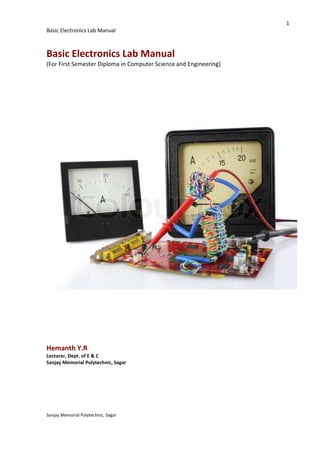
  • 1. Basic Electronics Lab Manual Sanjay Memorial Polytechnic, Sagar Basic Electronics Lab Manual (For First Semester Diploma in Computer Science and Engineering) Hemanth Y.R Lecturer, Dept. of E & C Sanjay Memorial Polytechnic, Sagar Sanjay Memorial Polytechnic, Sagar Basic Electronics Lab Manual Diploma in Computer Science and Engineering) Sagar 1
  • 2. 2 Basic Electronics Lab Manual Sanjay Memorial Polytechnic, Sagar GENERAL OBJECTIVES: No. of Hrs On completion of the lab course, the student will be able to 96 1 Comprehend the art of Soldering 2 Understand the behavioral characteristics of passive components GRADED EXERCISES: SECTION -- A STUDY EXERCISES Note: In Study Exercises the student should become familiar with specification of equipments & components & should draw a neat diagram of the control panel of equipment & actual appearance in case of components. Symbols should also be indicated wherever applicable 1 Familiarization and precautionary measures to be taken while using the following Equipments – Analog multimeter, Digital multimeter, Regulated power supply LCR Meter, Ammeters, Voltmeter and Galvanometer Ammeters voltmeter and Galvanometer 6 2 Identification of components ----- Passive and Active components with Symbol 6 3 Colour code--- Calculation of Resistance & Capacitance value by colour code method 6 4 Measurement of Resistance & Capacitance value by colour codes 6 5 Soldering Practice: Tool, Bending of Wires, Soldering of Passive and Active components 6 6 Testing of Passive Components 6 7 Familiarization, Study and Application of following Hardware materials and symbol FUSES --- Rewirable, Cartridge, High rupturing capacity Fuse KEYS--- Rectangular Buttons, Spring loaded, Mechanical , Electronic feather touch PLUGS AND SOCKETS--- 2 pin, 3 pin, Multiple, Round type CONNECTORS : IC and relay connector, PCB connector, BNC, threaded neutral modular TERMINALS ---Different sizes CABLES --- twisted pair, co-axial cable, optical cable CLIPS --- Crocodile , Banana Crimping tools 6 8 Study the block diagram of UPS & SMPS & state their merits and demerits 6 Total (Section A) 48
  • 3. 3 Basic Electronics Lab Manual Sanjay Memorial Polytechnic, Sagar SECTION -- B Conduction Exercises: 11 Verification of Ohm's law, 3 12 Verification of Kirchhoff's Current law for D.C Circuits 3 13 Verification of Kirchhoff's Voltage law for D.C Circuits 3 14 Characteristics of junction diode (Forward & Reverse Bias) 6 15 Characteristics of Zener diode (Forward & Reverse bias) 6 16 Inverting amplifier using OP-AMP 3 17 Non-inverting amplifier using OP-AMP 3 18 Half wave rectifier - construction, calculation of ripple factor with and without shunt capacitor filter 6 19 Full wave bridge rectifier - construction, calculation of ripple factor with and without shunt capacitor filter 9 Total (Section B) 48 Total 96 SCHEME OF VALUATION 1 Record 5 2 Part A - Study Exercise 25 3 Part B - Write up any One Experiment (Circuit Diagram, Tabular column, Formula ) 20 3 Construction using soldering and Conduction of Experiment 20 4 Result 10 5 Viva-Voce 20 Total 100
  • 4. 4 Basic Electronics Lab Manual Sanjay Memorial Polytechnic, Sagar SECTION -- A Study Exercises 1. Familiarization of meters. Connecting meters It is important to connect meters the correct way round: • The positive terminal of the meter, marked + or coloured red should be connected nearest to + on the battery or power supply. • The negative terminal of the meter, marked - or coloured black should be connected nearest to - on the battery or power supply. Voltmeters • Voltmeters measure voltage. • Voltage is measured in volts, V. • Voltmeters are connected in parallel across components. • Voltmeters have a very high resistance. Measuring voltage at a point When testing circuits you often need to find the voltages at various points, for example the voltage at pin 2 of a 555 timer IC. This can seem confusing - where should you connect the second voltmeter lead? • Connect the black (negative -) voltmeter lead to 0V, normally the negative terminal of the battery or power supply. • Connect the red (positive +) voltmeter lead to the point you where you need to measure the voltage. • The black lead can be left permanently connected to 0V while you use the red lead as a probe to measure voltages at various points. Connecting a voltmeter in parallel
  • 5. 5 Basic Electronics Lab Manual Sanjay Memorial Polytechnic, Sagar • You may wish to use a crocodile clip on the black lead to hold it in place. Voltage at a point really means the voltage difference between that point and 0V (zero volts) which is normally the negative terminal of the battery or power supply. Usually 0V will be labeled on the circuit diagram as a reminder. Analogue meters take a little power from the circuit under test to operate their pointer. This may upset the circuit and give an incorrect reading. To avoid this voltmeters should have a resistance of at least 10 times the circuit resistance (take this to be the highest resistor value near where the meter is connected). Most analogue voltmeters used in school science are not suitable for electronics because their resistance is too low, typically a few k . 100k or more is required for most electronics circuits. Ammeters • Ammeters measure current. • Current is measured in amps (amperes), A. 1A is quite large, so mA (milliamps) and µA (microamps) are often used. 1000mA = 1A, 1000µA = 1mA, 1000000µA = 1A. • Ammeters are connected in series. To connect in series you must break the circuit and put the ammeter across the gap, as shown in the diagram. • Ammeters have a very low resistance. The need to break the circuit to connect in series means that ammeters are difficult to use on soldered circuits. Most testing in electronics is done with voltmeters which can be easily connected without disturbing circuits. Galvanometers Galvanometers are very sensitive meters which are used to measure tiny currents, usually 1mA or less. They are used to make all types of analogue meters by adding suitable resistors as shown in the diagrams below. The photograph shows an educational 100µA galvanometer for which various multipliers and shunts are available. Connecting an ammeter in series
  • 6. 6 Basic Electronics Lab Manual Sanjay Memorial Polytechnic, Sagar Making a Voltmeter A galvanometer with a high resistance multiplier in series to make a voltmeter. Making an Ammeter A galvanometer with a low resistance shunt in parallel to make an ammeter. Galvanometer with multiplier and shunt Maximum meter current 100µA (or 20µA reverse). This meter is unusual in allowing small reverse readings to be shown. Ohmmeters An ohmmeter is used to measure resistance in ohms ( ). Ohmmeters are rarely found as separate meters but all standard multimeters have an ohmmeter setting. 1 is quite small so k and M are often used. 1k = 1000 , 1M = 1000k = 1000000 . Multimeters Multimeters are very useful test instruments. By operating a multi- position switch on the meter they can be quickly and easily set to be a voltmeter, an ammeter or an ohmmeter. They have several settings (called 'ranges') for each type of meter and the choice of AC or DC. Some multimeters have additional features such as transistor testing and ranges for measuring capacitance and frequency. Analogue multimeters consist of a galvanometer with various resistors which can be switched in as multipliers (voltmeter ranges) and shunts (ammeter ranges). Analogue Multimeter Digital Multimeter Multimeter Photographs © Rapid Electronics
  • 7. 7 Basic Electronics Lab Manual Sanjay Memorial Polytechnic, Sagar 2. Electronic Components and symbols 1. ACTIVE components increase the power of a signal and must be supplied with the signal and a source of power. Examples are bipolar transistors, field effect transistors etc. The signal is fed into one connection of the active device and the amplified version taken from another connection. In a transistor, the signal can be applied to the base connection and the amplified version taken from the collector. 2. PASSIVE components do not increase the power of a signal. They often cause power to be lost. Some can increase the voltage at the expense of current, so overall there is a loss of power. Resistors, capacitors, inductors and diodes are examples of passive components. Some of the active components are 1. Diodes 2. Transistors 3. Integrated circuits 4. Optoelectronic components Similarly some of the passive components are 1. Resistors 2. Capacitors 3. Inductors 4. Sensors 5. Detectors 6. Antennas Wires and connections Component Circuit Symbol Function of Component Wire To pass current very easily from one part of a circuit to another. Wires joined A 'blob' should be drawn where wires are connected (joined), but it is sometimes omitted. Wires connected at 'crossroads' should be staggered slightly to form two T- junctions, as shown on the right.
  • 8. 8 Basic Electronics Lab Manual Sanjay Memorial Polytechnic, Sagar Wires not joined In complex diagrams it is often necessary to draw wires crossing even though they are not connected. The simple crossing on the left is correct but may be misread as a join where the 'blob' has been forgotten. The bridge symbol on the right leaves no doubt! Power Supplies Component Circuit Symbol Function of Component Cell Supplies electrical energy. The larger terminal (on the left) is positive (+). A single cell is often called a battery, but strictly a battery is two or more cells joined together. Battery Supplies electrical energy. A battery is more than one cell. The larger terminal (on the left) is positive (+). Solar Cell Converts light to electrical energy. The larger terminal (on the left) is positive (+). DC supply Supplies electrical energy. DC = Direct Current, always flowing in one direction. AC supply Supplies electrical energy. AC = Alternating Current, continually changing direction. Fuse A safety device which will 'blow' (melt) if the current flowing through it exceeds a specified value. Transformer Two coils of wire linked by an iron core. Transformers are used to step up (increase) and step down (decrease) AC voltages. Energy is transferred between the coils by the magnetic field in the core. There is no electrical connection between the coils. Earth (Ground) A connection to earth. For many electronic circuits this is the 0V (zero volts) of the power supply, but for mains electricity and some radio circuits it really means the earth. It is also known as ground.
  • 9. 9 Basic Electronics Lab Manual Sanjay Memorial Polytechnic, Sagar Output Devices: Lamps, Heater, Motor, etc. Component Circuit Symbol Function of Component Lamp (lighting) A transducer which converts electrical energy to light. This symbol is used for a lamp providing illumination, for example a car headlamp or torch bulb. Lamp (indicator ) A transducer which converts electrical energy to light. This symbol is used for a lamp which is an indicator, for example a warning light on a car dashboard. Heater A transducer which converts electrical energy to heat. Motor A transducer which converts electrical energy to kinetic energy (motion). Bell A transducer which converts electrical energy to sound. Buzzer A transducer which converts electrical energy to sound. Inductor (Coil, Solenoid) A coil of wire which creates a magnetic field when current passes through it. It may have an iron core inside the coil. It can be used as a transducer converting electrical energy to mechanical energy by pulling on something. Switches Component Circuit Symbol Function of Component Push Switch (push-to- make) A push switch allows current to flow only when the button is pressed. This is the switch used to operate a doorbell. Push-to-Break Switch This type of push switch is normally closed (on), it is open (off) only when the button is pressed. On-Off Switch (SPST) SPST = Single Pole, Single Throw. An on-off switch allows current to flow only when it is in the closed (on) position.
  • 10. 10 Basic Electronics Lab Manual Sanjay Memorial Polytechnic, Sagar 2-way Switch (SPDT) SPDT = Single Pole, Double Throw. A 2-way changeover switch directs the flow of current to one of two routes according to its position. Some SPDT switches have a central off position and are described as 'on-off-on'. Dual On-Off Switch (DPST) DPST = Double Pole, Single Throw. A dual on-off switch which is often used to switch mains electricity because it can isolate both the live and neutral connections. Reversing Switch (DPDT) DPDT = Double Pole, Double Throw. This switch can be wired up as a reversing switch for a motor. Some DPDT switches have a central off position. Relay An electrically operated switch, for example a 9V battery circuit connected to the coil can switch a 230V AC mains circuit. NO = Normally Open, COM = Common, NC = Normally Closed. Resistors Component Circuit Symbol Function of Component Resistor A resistor restricts the flow of current, for example to limit the current passing through an LED. A resistor is used with a capacitor in a timing circuit. Some publications use the old resistor symbol: Variable Resistor (Rheostat) This type of variable resistor with 2 contacts (a rheostat) is usually used to control current. Examples include: adjusting lamp brightness, adjusting motor speed, and adjusting the rate of flow of charge into a capacitor in a timing circuit. Variable Resistor (Potentiometer) This type of variable resistor with 3 contacts (a potentiometer) is usually used to control voltage. It can be used like this as a transducer converting position (angle of the control spindle) to an electrical signal.
  • 11. 11 Basic Electronics Lab Manual Sanjay Memorial Polytechnic, Sagar Variable Resistor (Preset) This type of variable resistor (a preset) is operated with a small screwdriver or similar tool. It is designed to be set when the circuit is made and then left without further adjustment. Presets are cheaper than normal variable resistors so they are often used in projects to reduce the cost. Capacitors Component Circuit Symbol Function of Component Capacitor A capacitor stores electric charge. A capacitor is used with a resistor in a timing circuit. It can also be used as a filter, to block DC signals but pass AC signals. Capacitor, polarised A capacitor stores electric charge. This type must be connected the correct way round. A capacitor is used with a resistor in a timing circuit. It can also be used as a filter, to block DC signals but pass AC signals. Variable Capacitor A variable capacitor is used in a radio tuner. Trimmer Capacitor This type of variable capacitor (a trimmer) is operated with a small screwdriver or similar tool. It is designed to be set when the circuit is made and then left without further adjustment. Diodes Component Circuit Symbol Function of Component Diode A device which only allows current to flow in one direction. LED Light Emitting Diode A transducer which converts electrical energy to light. Zener Diode A special diode which is used to maintain a fixed voltage across its terminals. Photodiode A light-sensitive diode.
  • 12. 12 Basic Electronics Lab Manual Sanjay Memorial Polytechnic, Sagar Transistors Component Circuit Symbol Function of Component Transistor NPN A transistor amplifies current. It can be used with other components to make an amplifier or switching circuit. Transistor PNP A transistor amplifies current. It can be used with other components to make an amplifier or switching circuit. Phototransistor A light-sensitive transistor. Audio and Radio Devices Component Circuit Symbol Function of Component Microphone A transducer which converts sound to electrical energy. Earphone A transducer which converts electrical energy to sound. Loudspeaker A transducer which converts electrical energy to sound. Piezo Transducer A transducer which converts electrical energy to sound. Amplifier (general symbol) An amplifier circuit with one input. Really it is a block diagram symbol because it represents a circuit rather than just one component.
  • 13. 13 Basic Electronics Lab Manual Sanjay Memorial Polytechnic, Sagar Aerial (Antenna) A device which is designed to receive or transmit radio signals. It is also known as an antenna. Meters and Oscilloscope Component Circuit Symbol Function of Component Voltmeter A voltmeter is used to measure voltage. The proper name for voltage is 'potential difference', but most people prefer to say voltage! Ammeter An ammeter is used to measure current. Galvanometer A galvanometer is a very sensitive meter which is used to measure tiny currents, usually 1mA or less. Ohmmeter An ohmmeter is used to measure resistance. Most multimeters have an ohmmeter setting. Oscilloscope An oscilloscope is used to display the shape of electrical signals and it can be used to measure their voltage and time period. Sensors (input devices) Component Circuit Symbol Function of Component LDR A transducer which converts brightness (light) to resistance (an electrical property). LDR = Light Dependent Resistor Thermistor A transducer which converts temperature (heat) to resistance (an electrical property).
  • 14. 14 Basic Electronics Lab Manual Sanjay Memorial Polytechnic, Sagar 3. Colour code Resistor values - the resistor colour code Resistance is measured in ohms, the symbol for ohm is an omega . 1 is quite small so resistor values are often given in k and M . 1 k = 1000 1 M = 1000000 . Resistor values are normally shown using coloured bands. Each colour represents a number as shown in the table. Most resistors have 4 bands: • The first band gives the first digit. • The second band gives the second digit. • The third band indicates the number of zeros. • The fourth band is used to shows the tolerance (precision) of the resistor, this may be ignored for almost all circuits but further details are given below. This resistor has red (2), violet (7), yellow (4 zeros) and gold bands. So its value is 270000 = 270 k . On circuit diagrams the is usually omitted and the value is written 270K. Small value resistors (less than 10 ohm) The standard colour code cannot show values of less than 10 . To show these small values two special colours are used for the third band: gold which means × 0.1 and silver which means × 0.01. The first and second bands represent the digits as normal. For example: red, violet, gold bands represent 27 × 0.1 = 2.7 green, blue, silver bands represent 56 × 0.01 = 0.56 Tolerance of resistors (fourth band of colour code) The tolerance of a resistor is shown by the fourth band of the colour code. Tolerance is the precision of the resistor and it is given as a percentage. For example a 390 resistor with a tolerance of ±10% will have a value within 10% of 390 , between 390 - 39 = 351 and 390 + 39 = 429 (39 is 10% of 390). The Resistor Colour Code Colour Number Black 0 Brown 1 Red 2 Orange 3 Yellow 4 Green 5 Blue 6 Violet 7 Grey 8 White 9
  • 15. 15 Basic Electronics Lab Manual Sanjay Memorial Polytechnic, Sagar A special colour code is used for the fourth band tolerance: silver ±10%, gold ±5%, red ±2%, brown ±1%. If no fourth band is shown the tolerance is ±20%. Tolerance may be ignored for almost all circuits because precise resistor values are rarely required. Resistor shorthand Resistor values are often written on circuit diagrams using a code system which avoids using a decimal point because it is easy to miss the small dot. Instead the letters R, K and M are used in place of the decimal point. To read the code: replace the letter with a decimal point, then multiply the value by 1000 if the letter was K, or 1000000 if the letter was M. The letter R means multiply by 1. For example: 560R means 560 2K7 means 2.7 k = 2700 39K means 39 k 1M0 means 1.0 M = 1000 k
  • 16. 16 Basic Electronics Lab Manual Sanjay Memorial Polytechnic, Sagar 4. Soldering What is solder? Traditional solder is an alloy (mixture) of tin and lead, typically 60% tin and 40% lead. It melts at a temperature of about 200°C. Modern lead-free solder is an alloy of tin with other metals including copper and silver. It melts at a temperature of about 220°C. Coating a surface with solder is called 'tinning' because of the tin content of solder. Desoldering At some stage you will probably need to desolder a joint to remove or re-position a wire or component. There are two ways to remove the solder: 1. With a desoldering pump (solder sucker) • Set the pump by pushing the spring-loaded plunger down until it locks. • Apply both the pump nozzle and the tip of your soldering iron to the joint. • Wait a second or two for the solder to melt. • Then press the button on the pump to release the plunger and suck the molten solder into the tool. • Repeat if necessary to remove as much solder as possible. • The pump will need emptying occasionally by unscrewing the nozzle. How to Solder First a few safety precautions: • Never touch the element or tip of the soldering iron. They are very hot (about 400°C) and will give you a nasty burn. • Take great care to avoid touching the mains flex with the tip of the iron. The iron should have a heatproof flex for extra protection. An ordinary plastic flex will melt immediately if touched by a hot iron and there is a serious risk of burns and electric shock. • Always return the soldering iron to its stand when not in use. Never put it down on your workbench, even for a moment! Using a desoldering pump (solder sucker)
  • 17. 17 Basic Electronics Lab Manual Sanjay Memorial Polytechnic, Sagar • Work in a well-ventilated area. The smoke formed as you melt solder is mostly from the flux and quite irritating. Avoid breathing it by keeping you head to the side of, not above, your work. • Wash your hands after using solder. Traditional solder contains lead which is a poisonous metal. Preparing the soldering iron: • Place the soldering iron in its stand and plug in. The iron will take a few minutes to reach its operating temperature of about 400°C. • Dampen the sponge in the stand. The best way to do this is to lift it out the stand and hold it under a cold tap for a moment, then squeeze to remove excess water. It should be damp, not dripping wet. • Wait a few minutes for the soldering iron to warm up. You can check if it is ready by trying to melt a little solder on the tip. • Wipe the tip of the iron on the damp sponge. This will clean the tip. • Melt a little solder on the tip of the iron. This is called 'tinning' and it will help the heat to flow from the iron's tip to the joint. It only needs to be done when you plug in the iron, and occasionally while soldering if you need to wipe the tip clean on the sponge. You are now ready to start soldering: • Hold the soldering iron like a pen, near the base of the handle. Imagine you are going to write your name! Remember to never touch the hot element or tip. • Touch the soldering iron onto the joint to be made. Make sure it touches both the component lead and the track. Hold the tip there for a few seconds and... • Feed a little solder onto the joint. It should flow smoothly onto the lead and track to form a volcano shape as shown in the diagram. Apply the solder to the joint, not the iron. • Remove the solder, then the iron, while keeping the joint still. Allow the joint a few seconds to cool before you move the circuit board. • Inspect the joint closely. It should look shiny and have a 'volcano' shape. If not, you will need to reheat it and feed in a little more solder. This time ensure that both the lead and track are heated fully before applying solder.
  • 18. 18 Basic Electronics Lab Manual Sanjay Memorial Polytechnic, Sagar SECTION -- B Conduction Exercises Experiment No. 1 Verification of Ohm's law Aim of the Experiment: To study the dependence of current (I) on the potential difference (V) across a resistor and determine its resistance. Also plot a graph between V and I. In this lab, you will verify Ohms Law for different values of voltage and resistances. You will measure the true resistance of each resistor and the voltage applied to each resistor. You will then calculate the predicted current through each resistor. Finally, you will measure the actual current through each resistor to verify (or disprove!) Ohm’s Law. Equipments & Components Required: 1. Rheostat or Decade resistance box. 2. Regulated power supply. 3. Connecting wires. 4. Multimeter. Theory: The Ohm’s law states that the direct current flowing in a conductor is directly proportional to the potential difference between its ends. It is usually formulated as V = IR, where V is the potential difference, or voltage, I is the current, and R is the resistance of the conductor.
  • 19. Basic Electronics Lab Manual Sanjay Memorial Polytechnic, Sagar Consider the circuit shown below The resistance of that circuit would be given by R=V/I The current flowing through the circuit would be given by The voltage would be given by I x R Following figure shows graph of Voltage V/s Current Experiment: Circuit Diagram: Sanjay Memorial Polytechnic, Sagar Consider the circuit shown below The resistance of that circuit would be given by R=V/I = 24/2 = 12 ohms The current flowing through the circuit would be given by V/IR 24/12 = 2amps The voltage would be given by I x R = 2 x 12 = 24 volts Following figure shows graph of Voltage V/s Current 19 24/2 = 12 ohms V/IR 24/12 = 2amps
  • 20. 20 Basic Electronics Lab Manual Sanjay Memorial Polytechnic, Sagar Data Table: Resistance R = 1 KΩ Resistance R = 2 KΩ Trial No. Voltage V Applied in Volts Current I Thro’ R in mili amps Current I By Ohm’s Law I=V/R Trial No. Voltage V Applied in Volts Current I Thro’ R in mili amps Current I By Ohm’s Law I=V/R 1 1 1 1 2 2 2 2 3 3 3 3 4 4 4 4 5 5 5 5 6 6 6 6 7 7 7 7 8 8 8 8 9 9 9 9 10 10 10 10 Calculations Here ↓:
  • 21. 21 Basic Electronics Lab Manual Sanjay Memorial Polytechnic, Sagar Procedure: 1. Before doing the connection, check all the components and equipments. 2. Make the connection as shown in the circuit diagram. 3. Keep value of Rheostat or DRB to 1 KΩ and start first set of ten trials. 4. Vary voltage applied across R from 1V to 10V and record corresponding values of current from the ammeter. 5. Also calculate theoretical values of current using ohm’s law and record in the data table. 6. Observe the difference between theoretical and practical values of current. 7. Repeat from step 3 by keeping value of Rheostat or DRB to 2 K Ohm. Results:
  • 22. Basic Electronics Lab Manual Sanjay Memorial Polytechnic, Sagar Verification of Kirch Aim of the Experiment: To verify Kirchhoff’s current law. Equipments & Components Required: 1. Two fixed value resistors. 2. Regulated power supply. 3. Connecting wires. 4. Ammeter or Multimeter. Theory: Kirchhoff's first law, Kirchhoff's point rule states that at any node (junction) in an electrical circuit, the sum of currents flowing into that node is equal to the sum of currents flowing out of that currents in a network of conductors meeting at a point is zero. The current entering any junction is equal to the current leaving that junction. i2 + i3 = i1 + i4 Experiment No. 2 Verification of Kirchhoff's Current law for D.C Circuits To verify Kirchhoff’s current law. Equipments & Components Required: Two fixed value resistors. Regulated power supply. Multimeter. Kirchhoff's point rule, or Kirchhoff's junction rule at any node (junction) in an electrical circuit, the sum of currents flowing into that node is equal to the sum of currents flowing out of that node or the algebraic sum of currents in a network of conductors meeting at a point is zero. The current entering any junction is equal to the current leaving that junction. 22 off's Current law for D.C Circuits Kirchhoff's junction rule (or nodal rule) at any node (junction) in an electrical circuit, the sum of currents flowing into node or the algebraic sum of The current entering any junction is equal to the current leaving that junction.
  • 23. 23 Basic Electronics Lab Manual Sanjay Memorial Polytechnic, Sagar Experiment: Circuit Diagram: Current Equations: Equivalent Resistance REQU = (R1*R2) / (R1+R2) Total Current I = V/ REQU Current Thro’ R1 is I1 = V/ R1 Current Thro’ R2 is I2= V/ R2 Data Table: Trial No. Voltage V Applied in Volts Theoretical Values Practical Values Current I in mili amps Current I1 in mili amps Current I2 in mili amps Current I in mili amps Current I1 in mili amps Current I2 in mili amps 1 0 2 5 3 10 4 15 5 20 6 25 7 30 V 30V R1 1.0kohm R2 2.0kohm 0.045 A + - 0.030 A + - 0.015 A + -
  • 24. 24 Basic Electronics Lab Manual Sanjay Memorial Polytechnic, Sagar Calculations Here ↓: Procedure: 1. Before doing the connection, check all the components and equipments. 2. Make the connection as shown in the circuit diagram. 3. Take two fixed value resistors R1 and R2. 4. Vary voltage applied from 0V to 30V in steps of 5V and record corresponding values of currents I, I1 and I2 from corresponding ammeters. 5. Also calculate theoretical values of current using equations given above and record in the data table. 6. Observe the difference between theoretical and practical values of currents. Results:
  • 25. 25 Basic Electronics Lab Manual Sanjay Memorial Polytechnic, Sagar Experiment No. 3 Verification of Kirchhoff's Voltage law for D.C Circuits Aim of the Experiment: To verify Kirchhoff’s voltage law. Equipments & Components Required: 1. Two fixed value resistors. 2. Regulated power supply. 3. Connecting wires. 4. Ammeter or Multimeter. Theory: Kirchhoff's second law, Kirchhoff's loop (or mesh) rule states that the algebraic sum of the voltage (potential) differences in any loop must equal zero. If we consider a closed loop, conventionally if we consider all the voltage gains along the loop are positive then all the voltage drops along the loop should be considered as negative. The summation of all these voltages in a closed loop is equal to zero. Suppose n numbers of back to back connected elements form a closed loop. Among these circuit element m number elements are voltage source and n – m number of elements are resistors then, The voltages of sources are V1, V2, V3,………………. Vm and voltage drops across the resistors respectively, Vm + 1, Vm + 2, Vm + 3,………………… Vn.
  • 26. 26 Basic Electronics Lab Manual Sanjay Memorial Polytechnic, Sagar As it said that the voltage gain conventionally considered as positive, and voltage drops are considered as negative, the voltages along the closed loop are + V1, + V2, + V3,………………. + Vm, − Vm + 1, − Vm + 2, − Vm + 3,…………………− Vn. Now according to Kirchhoff Voltage law the summation of all these voltages results to zero. That means, V1 + V2 + V3 + …………. + Vm − Vm + 1 − Vm + 2 − Vm + 3 + ……………− Vn = 0 So accordingly Kirchhoff Second Law, ∑V = 0 Experiment: Circuit Diagram: Current and Voltage Equations: Equivalent Resistance REQU = R1+R2 Total Current I = V/ REQU Voltage across R1 is V1 = I * R1 Voltage across R2 is V2 = I * R2 V 30V R1 1.0kohm R2 2.0kohm 0.010 A + - 10.007 V + - 19.993 V + -
  • 27. 27 Basic Electronics Lab Manual Sanjay Memorial Polytechnic, Sagar Data Table: Trial No. Voltage V Applied in Volts Theoretical Values Practical Values Current I in mili amps Voltage V1 in Volts Voltage V2 in Volts Current I in mili amps Voltage V1 in Volts Voltage V2 in Volts 1 0 2 5 3 10 4 15 5 20 6 25 7 30 Calculations Here ↓:
  • 28. 28 Basic Electronics Lab Manual Sanjay Memorial Polytechnic, Sagar Procedure: 1. Before doing the connection, check all the components and equipments. 2. Make the connection as shown in the circuit diagram. 3. Take two fixed value resistors R1 and R2. 4. Vary voltage applied from 0V to 30V in steps of 5V and record corresponding values of currents I, V1 and V2 from corresponding meters. 5. Also calculate theoretical values of current I, Voltages V1 and V2 using equations given above and record in the data table. 6. Observe the difference between theoretical and practical values. Results:
  • 29. Basic Electronics Lab Manual Sanjay Memorial Polytechnic, Sagar Characteristics of junction diode (Forward & Reverse Bias) Aim of the Experiment: To study characteristics of junction diode in both forward and reverse Equipments & Components Required: 1. Resistors - 1K 2. Diode – BY127, 1N4001, …, 1N4007 3. Regulated power supply. 4. Connecting wires. 5. Ammeter and Multimeter. Theory: A diode is a two-terminal low (ideally zero) resistance resistance in the other. A p–n junction diode is made of a crystal of it to create a region on one side that contains negative type semiconductor, and a region on the other side that contains positive charge carriers (holes), called p-type semiconductor attached together, a momentary flow of electrons occur from n to p side resulti region where no charge carriers are present. It is called Depletion region due to the absence of charge carriers (electrons and holes in this case). The diode's terminals are attached to each of these regions. The boundary between these two r where the action of the diode takes place. The crystal allows electrons to flow from the N type side (called the cathode direction. The symbol used for a semiconductor diode in a diode. There are alternate symbols for some types of diodes, though the differences are minor. Diode LED Zener Diode Tunnel Diode Sanjay Memorial Polytechnic, Sagar Experiment No. 4 Characteristics of junction diode (Forward & Reverse Bias) To study characteristics of junction diode in both forward and reverse Equipments & Components Required: 1KΩ BY127, 1N4001, …, 1N4007 Regulated power supply. Connecting wires. Multimeter. terminal electronic component with asymmetric resistance to current flow in one direction, and high (ideally n junction diode is made of a crystal of semiconductor. Impurities are added to it to create a region on one side that contains negative charge carriers , and a region on the other side that contains positive charge carriers type semiconductor. When two materials i.e. n- attached together, a momentary flow of electrons occur from n to p side resulti region where no charge carriers are present. It is called Depletion region due to the absence of charge carriers (electrons and holes in this case). The diode's terminals are attached to each of these regions. The boundary between these two regions, called a where the action of the diode takes place. The crystal allows electrons to flow from the N cathode) to the P-type side (called the anode), but not in the opposite The symbol used for a semiconductor diode in a circuit diagram diode. There are alternate symbols for some types of diodes, though the differences are Photo Diode Schottky diode Tunnel Diode Varicap 29 Characteristics of junction diode (Forward & Reverse Bias) To study characteristics of junction diode in both forward and reverse bias condition. with asymmetric conductance, it has nt flow in one direction, and high (ideally infinite) . Impurities are added to charge carriers (electrons), called n- , and a region on the other side that contains positive charge carriers type and p-type are attached together, a momentary flow of electrons occur from n to p side resulting in a third region where no charge carriers are present. It is called Depletion region due to the absence of charge carriers (electrons and holes in this case). The diode's terminals are attached to egions, called a p–n junction, is where the action of the diode takes place. The crystal allows electrons to flow from the N- ), but not in the opposite circuit diagram specifies the type of diode. There are alternate symbols for some types of diodes, though the differences are Schottky diode
  • 30. 30 Basic Electronics Lab Manual Sanjay Memorial Polytechnic, Sagar Junction Diode Symbol and Static I-V Characteristics. Forward Biased Junction Diode When a diode is connected in a Forward Bias condition, a negative voltage is applied to the N-type material and a positive voltage is applied to the P-type material. If this external voltage becomes greater than the value of the potential barrier, approx. 0.7 volts for silicon and 0.3 volts for germanium, the potential barriers opposition will be overcome and current will start to flow. This is because the negative voltage pushes or repels electrons towards the junction giving them the energy to cross over and combine with the holes being pushed in the opposite direction towards the junction by the positive voltage. This results in a characteristics curve of zero current flowing up to this voltage point, called the "knee" on the static curves and then a high current flow through the diode with little increase in the external voltage as shown below. Forward Characteristics Curve for a Junction Diode
  • 31. 31 Basic Electronics Lab Manual Sanjay Memorial Polytechnic, Sagar The application of a forward biasing voltage on the junction diode results in the depletion layer becoming very thin and narrow which represents a low impedance path through the junction thereby allowing high currents to flow. The point at which this sudden increase in current takes place is represented on the static I-V characteristics curve above as the "knee" point. Forward Biased Junction Diode showing a Reduction in the Depletion Layer This condition represents the low resistance path through the PN junction allowing very large currents to flow through the diode with only a small increase in bias voltage. The actual potential difference across the junction or diode is kept constant by the action of the depletion layer at approximately 0.3v for germanium and approximately 0.7v for silicon junction diodes. Since the diode can conduct "infinite" current above this knee point as it effectively becomes a short circuit, therefore resistors are used in series with the diode to limit its current flow. Exceeding its maximum forward current specification causes the device to dissipate more power in the form of heat than it was designed for resulting in a very quick failure of the device. Reverse Biased Junction Diode When a diode is connected in a Reverse Bias condition, a positive voltage is applied to the N-type material and a negative voltage is applied to the P-type material. The positive voltage applied to the N-type material attracts electrons towards the positive electrode and away from the junction, while the holes in the P-type end are also attracted away from the junction towards the negative electrode. The net result is that the depletion layer grows wider due to a lack of electrons and holes and presents a high impedance path, almost an insulator. The result is that a high potential barrier is created thus preventing current from flowing through the semiconductor material.
  • 32. 32 Basic Electronics Lab Manual Sanjay Memorial Polytechnic, Sagar Reverse Biased Junction Diode showing an Increase in the Depletion Layer This condition represents a high resistance value to the PN junction and practically zero current flows through the junction diode with an increase in bias voltage. However, a very small leakage current does flow through the junction which can be measured in microamperes, (μA). One final point, if the reverse bias voltage Vr applied to the diode is increased to a sufficiently high enough value, it will cause the PN junction to overheat and fail due to the avalanche effect around the junction. This may cause the diode to become shorted and will result in the flow of maximum circuit current, and this shown as a step downward slope in the reverse static characteristics curve below. Reverse Characteristics Curve for a Junction Diode Sometimes this avalanche effect has practical applications in voltage stabilising circuits where a series limiting resistor is used with the diode to limit this reverse breakdown current to a preset maximum value thereby producing a fixed voltage output across the diode. These types of diodes are commonly known as Zener Diodes and are discussed in a later tutorial.
  • 33. 33 Basic Electronics Lab Manual Sanjay Memorial Polytechnic, Sagar Experiment: Circuit Diagram: Forward Biased Junction Diode Data Table: Trial No. Forward Voltage Vd In Volts Forward Current Id in mili amps 1 0.1 2 0.2 3 0.3 4 0.4 5 0.5 6 0.6 7 0.7 8 0.8 9 0.9 10 1.0 V1 30V R1 1.0kohm 0.029 A + - 0.668 V + - D1 1N4001GP
  • 34. 34 Basic Electronics Lab Manual Sanjay Memorial Polytechnic, Sagar Reverse Biased Junction Diode Data Table: Trial No. Reverse Voltage Vr In Volts Reverse Current Ir in micro amps 1 2 2 4 3 6 4 8 5 10 6 12 7 14 8 16 9 18 10 20 V1 30V R1 1.0kohm 0.028m A + - 29.969 V + - D1 1N4001GP
  • 35. 35 Basic Electronics Lab Manual Sanjay Memorial Polytechnic, Sagar Procedure: 1. Before doing the connection, check all the components and equipments. 2. Make the connection as shown in the circuit diagram. 3. Vary the applied voltage in both forward and reverse bias as given in the data table. 4. Record forward and reverse currents in both forward and reverse conditions. 5. Plot a graph for both forward and reverse bias conditions by taking voltage along the X-axis and current along Y-axis Results:
  • 36. 36 Basic Electronics Lab Manual Sanjay Memorial Polytechnic, Sagar Experiment No. 5 Characteristics of zener diode (Forward & Reverse Bias) Aim of the Experiment: To study characteristics of zener diode in both forward and reverse bias condition. Equipments & Components Required: 1. Resistors - 1KΩ 2. Zener Diode 3. Regulated power supply. 4. Connecting wires. 5. Ammeter and Multimeter. Theory: A Zener diode is a diode which allows current to flow in the forward direction in the same manner as an ideal diode, but will also permit it to flow in the reverse direction when the voltage is above a certain value known as the breakdown voltage, "zener knee voltage", "zener voltage" or "avalanche point". A conventional solid-state diode will allow significant current if it is reverse-biased above its reverse breakdown voltage. When the reverse bias breakdown voltage is exceeded, a conventional diode is subject to high current due to avalanche breakdown. Unless this current is limited by circuitry, the diode will be permanently damaged due to overheating. A zener diode exhibits almost the same properties, except the device is specially designed so as to have a reduced breakdown voltage, the so-called zener voltage. By contrast with the conventional device, a reverse-biased zener diode will exhibit a controlled breakdown and allow the current to keep the voltage across the zener diode close to the zener breakdown voltage. For example, a diode with a zener breakdown voltage of 3.2 V will exhibit a voltage drop of very nearly 3.2 V across a wide range of reverse currents. The zener diode is therefore ideal for applications such as the generation of a reference voltage (e.g. for an amplifier stage), or as a voltage stabilizer for low-current applications. Example: Circuit symbol: a = anode, k = cathode Zener diodes are used to maintain a fixed voltage. They are designed to 'breakdown' in a reliable and non-destructive way so that they can be used in reverse to maintain a fixed voltage across their terminals. The diagram shows how they are connected, with a resistor in series to limit the current.
  • 37. 37 Basic Electronics Lab Manual Sanjay Memorial Polytechnic, Sagar Zener diodes can be distinguished from ordinary diodes by their code and breakdown voltage which are printed on them. Zener diode codes begin BZX... or BZY... Their breakdown voltage is printed with V in place of a decimal point, so 4V7 means 4.7V for example. Zener diodes are rated by their breakdown voltage and maximum power: • The minimum voltage available is 2.4V. • Power ratings of 400mW and 1.3W are common. Zener Diode Symbol and Static I-V Characteristics.
  • 38. 38 Basic Electronics Lab Manual Sanjay Memorial Polytechnic, Sagar Experiment: Circuit Diagram: Forward Biased Zener Diode Data Table: Trial No. Forward Voltage Vd In Volts Forward Current Id in mili amps 1 0.1 2 0.2 3 0.3 4 0.4 5 0.5 6 0.6 7 0.7 8 0.8 9 0.9 10 1.0 V1 30V R1 1.0kohm 0.029 A + - 0.627 V + - D1 RD4.7
  • 39. 39 Basic Electronics Lab Manual Sanjay Memorial Polytechnic, Sagar Reverse Biased Zener Diode Data Table: Trial No. Reverse Voltage Vr In Volts Reverse Current Ir in micro amps 1 2 2 4 3 6 4 8 5 10 6 12 7 14 8 16 9 18 10 20 V1 10V R1 1.0kohm 5.034m A + - 4.965 V + - D1 RD4.7
  • 40. 40 Basic Electronics Lab Manual Sanjay Memorial Polytechnic, Sagar Procedure: 1. Before doing the connection, check all the components and equipments. 2. Make the connection as shown in the circuit diagram. 3. Vary the diode voltage in both forward and reverse bias as given in the data table. 4. Record forward and reverse currents in both forward and reverse conditions. 5. Plot a graph for both forward and reverse bias conditions by taking voltage along the X-axis and current along Y-axis Results:
  • 41. Basic Electronics Lab Manual Sanjay Memorial Polytechnic, Sagar Inverting amplifier using OP Aim of the Experiment: To study OP-AMP as an inverting amplifier Equipments & Components Required: 1. Resistors - 1K 2. OP-AMP - µA741 3. Regulated power supply. 4. Signal Generator 5. Connecting wires. 6. CRO. Theory: An operational amplifier (op amplifier with a differential input an op-amp produces an output potential (relative to circuit ground) that is typically hundreds of thousands of times larger than the potential difference between its input terminals. Circuit notation Circuit diagram symbol for an The circuit symbol for an op • V+: non-inverting input • V−: inverting input • Vout: output • VS+: positive power supply • VS−: negative power supply Sanjay Memorial Polytechnic, Sagar Experiment No. 6 Inverting amplifier using OP-AMP AMP as an inverting amplifier. Equipments & Components Required: 1KΩ & 10KΩ µA741 Regulated power supply. Signal Generator Connecting wires. An operational amplifier (op-amp) is a DC-coupled high-gain differential input and, usually, a single-ended output. In this amp produces an output potential (relative to circuit ground) that is typically hundreds of thousands of times larger than the potential difference between its input Circuit diagram symbol for an op-amp The circuit symbol for an op-amp is shown to the right, where: inverting input : inverting input : output : positive power supply : negative power supply 41 gain electronic voltage ended output. In this configuration, amp produces an output potential (relative to circuit ground) that is typically hundreds of thousands of times larger than the potential difference between its input
  • 42. Basic Electronics Lab Manual Sanjay Memorial Polytechnic, Sagar Operation An op-amp without negative feedback (a comparator) The amplifier's differential inputs consist of a op-amp amplifies only the difference in voltage between the two, which is called the differential input voltage. The output voltage of the op Where V+ is the voltage at the non inverting terminal and A loop" refers to the absence of a feedback loop from the output to the input). The magnitude of AOL is typically very large op-amps—and therefore even a quite small difference between V+ and V amplifier output nearly to the supply voltage. Situations in which the output voltage is equal to or greater than the supply voltage are referred to as saturation of the amplifier. The magnitude of AOL is not well controlled by the manufacturing process, and so it is impractical to use an operational amplifier as a stand amplifier. Without negative feedback inverting input is held at ground (0 V) directly or by a resistor, and the input voltage Vin applied to the non- positive; if Vin is negative, the output will be maximum negative. Since there is no feedback from the output to either input, this is an comparator. An op-amp with negative feedback (a non amp without negative feedback (a comparator) The amplifier's differential inputs consist of a V+ input and a V− input, and ideally the amp amplifies only the difference in voltage between the two, which is called the . The output voltage of the op-amp is given by the equa is the voltage at the non-inverting terminal, V− is the voltage at the AOL is the open-loop gain of the amplifier (the term "open loop" refers to the absence of a feedback loop from the output to the input). The magnitude of AOL is typically very large—100,000 or more for integrated circuit and therefore even a quite small difference between V+ and V amplifier output nearly to the supply voltage. Situations in which the output voltage ual to or greater than the supply voltage are referred to as saturation of the amplifier. The magnitude of AOL is not well controlled by the manufacturing process, and so it is impractical to use an operational amplifier as a stand-alone negative feedback, an op-amp acts as a comparator inverting input is held at ground (0 V) directly or by a resistor, and the input voltage -inverting input is positive, the output will be maximum tive; if Vin is negative, the output will be maximum negative. Since there is no feedback from the output to either input, this is an open loop circuit acti amp with negative feedback (a non-inverting amplifier) 42 input, and ideally the amp amplifies only the difference in voltage between the two, which is called the amp is given by the equation: is the voltage at the gain of the amplifier (the term "open- loop" refers to the absence of a feedback loop from the output to the input). 100,000 or more for integrated circuit and therefore even a quite small difference between V+ and V− drives the amplifier output nearly to the supply voltage. Situations in which the output voltage ual to or greater than the supply voltage are referred to as saturation of the amplifier. The magnitude of AOL is not well controlled by the manufacturing process, alone differential comparator. If the inverting input is held at ground (0 V) directly or by a resistor, and the input voltage inverting input is positive, the output will be maximum tive; if Vin is negative, the output will be maximum negative. Since there is no circuit acting as a inverting amplifier)
  • 43. Basic Electronics Lab Manual Sanjay Memorial Polytechnic, Sagar If predictable operation is desired, negative feedback is used, by applying a portion of the output voltage to the inverting input. The reduces the gain of the amplifier. When negative feedback is used, the circuit's overall gain and response becomes determined mostly by the feedback network rather than by the op For example, in a non negative feedback via the voltage divider Rf, Rg reduces the gain. Equilibrium will be established when Vout is just sufficient to reach around and "pull" the inverting input to the same voltage as Vin. The voltage gain of the entire circuit is determined by 1 + Rf/Rg. As a simple example, if Vin = 1V and Rf = Rg, Vout will be 2V, the amount required to keep V a closed loop circuit. Its overall gain Vout Because the feedback is negative, in this case ACL is less than the AOL of the op Another way of looking at it is to make two relatively valid assumptions. One, that when an op difference in voltage between the non small as to be considered negligible. The second assumption is that the input impedance at both (+) and extremely high (at least several megohms with modern op Thus, when the circuit to the right is operated as a non will appear at the (+) and ( Sinc Kirchhoff's current law states that the same current must leave a node as enter it, and since the impedance into the ( overwhelming majority of the same current i travels through Rf, creating an output voltage equal to Vin + i × Rf. By combining terms, we can easily determine the gain of this particular type of circuit. Sanjay Memorial Polytechnic, Sagar If predictable operation is desired, negative feedback is used, by applying a portion ltage to the inverting input. The closed loop reduces the gain of the amplifier. When negative feedback is used, the circuit's overall gain and response becomes determined mostly by the feedback network rather than by the op-amp itself. For example, in a non-inverting amplifier (see the figure on the right) adding a negative feedback via the voltage divider Rf, Rg reduces the gain. Equilibrium will be established when Vout is just sufficient to reach around and "pull" the inverting to the same voltage as Vin. The voltage gain of the entire circuit is determined by 1 + Rf/Rg. As a simple example, if Vin = 1V and Rf = Rg, Vout will be 2V, the amount required to keep V− at 1V. Because of the feedback provided by Rf, Rg this is loop circuit. Its overall gain Vout / Vin is called the closed Because the feedback is negative, in this case ACL is less than the AOL of the op Another way of looking at it is to make two relatively valid assumptions. n op-amp is being operated in linear (not saturated) mode, the difference in voltage between the non-inverting (+) pin and the inverting ( as to be considered negligible. The second assumption is that the input impedance at both (+) and extremely high (at least several megohms with modern op Thus, when the circuit to the right is operated as a non-inverting linear amplifier, Vin will appear at the (+) and (−) pins and create a current i through Rg equal to Vin/Rg. Kirchhoff's current law states that the same current must leave a node as enter it, and since the impedance into the (−) pin is near infinity, we can assume the overwhelming majority of the same current i travels through Rf, creating an output l to Vin + i × Rf. By combining terms, we can easily determine the gain of this particular type of circuit. 43 If predictable operation is desired, negative feedback is used, by applying a portion closed loop feedback greatly reduces the gain of the amplifier. When negative feedback is used, the circuit's overall gain and response becomes determined mostly by the feedback network inverting amplifier (see the figure on the right) adding a negative feedback via the voltage divider Rf, Rg reduces the gain. Equilibrium will be established when Vout is just sufficient to reach around and "pull" the inverting to the same voltage as Vin. The voltage gain of the entire circuit is determined by 1 + Rf/Rg. As a simple example, if Vin = 1V and Rf = Rg, Vout will be 2V, the − at 1V. Because of the feedback provided by Rf, Rg this is Vin is called the closed-loop gain ACL. Because the feedback is negative, in this case ACL is less than the AOL of the op-amp. Another way of looking at it is to make two relatively valid assumptions. amp is being operated in linear (not saturated) mode, the e inverting (−) pin is so The second assumption is that the input impedance at both (+) and (−) pins is extremely high (at least several megohms with modern op-amps). inverting linear amplifier, Vin −) pins and create a current i through Rg equal to Vin/Rg. Kirchhoff's current law states that the same current must leave a node as enter −) pin is near infinity, we can assume the overwhelming majority of the same current i travels through Rf, creating an output l to Vin + i × Rf. By combining terms, we can easily determine the gain of
  • 44. Basic Electronics Lab Manual Sanjay Memorial Polytechnic, Sagar Op-amp characteristics Ideal op-amps An ideal op-amp is usually considered to have the following properties: • Infinite open • Infinite voltage range available at the output • Infinite bandwidth with zero phase shift and infinite slew rate • Infinite input impedance and so zero input current and zero input offset voltage • Zero output impedance • Zero noise • Infinite Common • Infinite Power supply rejection ratio. These ideals can be summarized by the two "golden rules": I. The output attempts to do whatever is necessary to make the voltage difference between the inputs zero. II. The inputs draw no current Pin Diagram of µA741 Op amp is usually considered to have the following properties: Infinite open-loop gain. Infinite voltage range available at the output. Infinite bandwidth with zero phase shift and infinite slew rate Infinite input impedance and so zero input current and zero input offset voltage. Zero output impedance. Zero noise. Infinite Common-mode rejection ratio (CMRR). Infinite Power supply rejection ratio. These ideals can be summarized by the two "golden rules": I. The output attempts to do whatever is necessary to make the voltage difference between the inputs zero. II. The inputs draw no current. Pin Diagram of µA741 Op-Amp 44 amp is usually considered to have the following properties: Infinite bandwidth with zero phase shift and infinite slew rate. Infinite input impedance and so zero input current and zero input I. The output attempts to do whatever is necessary to make the
  • 45. 45 Basic Electronics Lab Manual Sanjay Memorial Polytechnic, Sagar Experiment: Circuit Diagram: Procedure: 1. Connect the circuit as shown in the circuit diagram. 2. Give the input signal as specified. 3. Switch on the power supply. 4. Note down the outputs from the CRO 5. Draw the necessary waveforms on the graph sheet. Observations: 1. Observe the output waveform from CRO. An inverted and amplified waveform will be observed. 2. Measure the input and output voltage from the input and output waveform in the CRO. 3. Calculate 4. Compare the theoretical voltage gain from the above equation with the experimental value obtained by dividing output voltage by input voltages observed. 5. Observe outputs of the inverting amplifier circuit using different input waveforms. Results: Pin 7 → +12V Pin 4 → -12V R1 = 1KΩ R2 = 10KΩ Gain = -R2/R1
  • 46. 46 Basic Electronics Lab Manual Sanjay Memorial Polytechnic, Sagar Experiment No. 7 Non-inverting amplifier using OP-AMP Aim of the Experiment: To study OP-AMP as non-inverting amplifier. Equipments & Components Required: 1. Resistors - 1KΩ & 10KΩ 2. OP-AMP - µA741 3. Regulated power supply. 4. Signal Generator 5. Connecting wires. 6. CRO. Theory: Same as Experiment no. 6. Experiment: Circuit Diagram: Procedure: 1. Connect the circuit as shown in the circuit diagram. 2. Give the input signal as specified. 3. Switch on the power supply. 4. Note down the outputs from the CRO 5. Draw the necessary waveforms on the graph sheet. Pin 7 → +12V Pin 4 → -12V R1 = 1KΩ R2 = 10KΩ Gain = 1+ (R2/R1)
  • 47. 47 Basic Electronics Lab Manual Sanjay Memorial Polytechnic, Sagar Observations: 1. Observe the output waveform from CRO. A non-inverted and amplified waveform will be observed. 2. Measure the input and output voltage from the input and output waveform in the CRO. 3. Calculate 4. Compare the theoretical voltage gain from the above equation with the experimental value obtained by dividing output voltage by input voltages observed. 5. Observe outputs of the inverting amplifier circuit using different input waveforms. Results:
  • 48. 48 Basic Electronics Lab Manual Sanjay Memorial Polytechnic, Sagar Experiment No. 8 Half wave rectifier - construction, calculation of ripple factor with and without shunt capacitor filter. Aim of the Experiment: To construct and calculate half wave rectifier with and without filter. Equipments & Components Required: 1. Resistors - 1KΩ 2. Step down transformer 3. Rectifier diode – BY 127, 1N4001… 4007. 4. Connecting wires. 5. CRO. Theory: Rectification is a process of converting ac to pulsating dc. Half wave rectifier convert ac to pulsating dc by simply allowing half of the input ac cycle to pass, while blocking current to prevent it from flowing during the other half cycle as shown below While the output of a rectifier is a pulsating dc that means it contains both ripples and dc components. Ripples are high frequency ac signals in the dc output of the rectifier. Most electronic circuits require a substantially pure dc for proper operation. This type of output is provided by single or multi-section filter circuits placed between the output of the rectifier and the load. Shunt Capacitor Filter This is the simplest form of the filter circuit and in this arrangement a high value capacitor C is placed directly across the output terminals, as shown in figure. During the conduction period capacitor gets charged and during non-conduction period it discharges. The time duration taken by capacitor C to get charged to peak value is negligible because there is no resistance (except the negligible forward resistance of diode) in the charging path. But the discharging time is quite large (roughly 100 times more than the charging time depending upon the value of RL) because it discharges through load resistance RL.
  • 49. Basic Electronics Lab Manual Sanjay Memorial Polytechnic, Sagar Experiment: Circuit Diagram: Half wave rectifier without filter Sanjay Memorial Polytechnic, Sagar Half wave rectifier without filter 49
  • 50. Basic Electronics Lab Manual Sanjay Memorial Polytechnic, Sagar ac voltage at o/p Ripple Factor = dc voltage at o/p Procedure: 1. Connect the primary side of the transformer to AC main as shown in the figure 2. Connect the C.R.O. probes to the output points. By proper setting of C.R.O. stable wave shape can be seen on its screen .Plot this wave form & wave shape at the op points. 3. Using multimeter measure AC and DC voltages at o/p points 4. Using the measured value of DC & AC output voltages, calculate Ripple factor .It should be near about 1.21 Results: Ripple Factor = Circuit Diagram: Half wave rectifier with filter Procedure: 1. Connect the primary side of the transformer to AC main as shown in the figure 2. Connect the C.R.O. probes to the output points. By proper setting stable wave shape can be seen on its screen .Plot this wave form & also observe the wave shape at the op points. . 3. Using multimeter measure AC and DC voltages at o/p points 4. Using the measured value of DC & AC output volta ac voltage at o/p = 1.21 (Theoretical) dc voltage at o/p primary side of the transformer to AC main as shown in the figure Connect the C.R.O. probes to the output points. By proper setting of C.R.O. table wave shape can be seen on its screen .Plot this wave form & also observe the p points. . Using multimeter measure AC and DC voltages at o/p points. Using the measured value of DC & AC output voltages, calculate Ripple factor .It should Half wave rectifier with filter primary side of the transformer to AC main as shown in the figure Connect the C.R.O. probes to the output points. By proper setting of C.R.O. table wave shape can be seen on its screen .Plot this wave form & also observe the p points. . Using multimeter measure AC and DC voltages at o/p points. Using the measured value of DC & AC output voltages, calculate Ripple factor. 50 primary side of the transformer to AC main as shown in the figure. Connect the C.R.O. probes to the output points. By proper setting of C.R.O. a good & also observe the Using the measured value of DC & AC output voltages, calculate Ripple factor .It should primary side of the transformer to AC main as shown in the figure. of C.R.O. a good & table wave shape can be seen on its screen .Plot this wave form & also observe the Ripple factor.
  • 51. Basic Electronics Lab Manual Sanjay Memorial Polytechnic, Sagar Full wave bridge rectifier Aim of the Experiment: To construct and calculate full wave Equipments & Components Required: 1. Resistors - 1K 2. Step down transformer 3. Rectifier diode – 4. Connecting wires. 5. CRO. Theory: Rectification is a process of converting ac to pulsating dc ac to pulsating dc by simply allow to prevent it from flowing during the other half cycle as shown below Sanjay Memorial Polytechnic, Sagar Experiment No. 9 rectifier - construction, calculation of ripple factor with and without shunt capacitor filter. To construct and calculate full wave bridge rectifier with and without filter. Equipments & Components Required: 1KΩ Step down transformer – BY 127, 1N4001… 4007. Connecting wires. Rectification is a process of converting ac to pulsating dc. Half wave rectifier simply allowing half of the input ac cycle to pass, while blocking current ing during the other half cycle as shown below 51 construction, calculation of ripple factor with and without filter. Half wave rectifier convert ac cycle to pass, while blocking current
  • 52. 52 Basic Electronics Lab Manual Sanjay Memorial Polytechnic, Sagar When the upper end of the transformer secondary winding is positive, say during first half-cycles of the input supply, diodes D1 and D3 are forward biased and current flows through arm AB, enters the load at positive terminal, leaves the load at negative terminal, and returns back flowing through arm DC. During this half of each input cycle, the diodes D2 and D4 are reverse biased and so the current is not allowed to flow in arms AD and BC. The flow of current is indicated by solid arrows in the figure. In the second half of the input cycle the lower end of ac supply becomes positive, diodes D2 and D4 become forward biased and current flows through arm CB, enters the load at the positive terminal, leaves the load at negative terminal and returns back flowing through arm DA. Flow of current has been shown by dotted arrows in the figure. Thus the direction of flow of current through the load resistance RL remains the same during both half cycles of the input supply voltage Experiment: Circuit Diagram: Full wave bridge rectifier without filter ܴ݅‫݈݁݌݌‬ ‫ݎ݋ݐܿܽܨ‬ ൌ ௔௖ ௩௢௟௧௔௚௘ ௔௧ ௢/௣ ௗ௖ ௩௢௟௧௔௚௘ ௔௧ ௢/௣ ൌ 0.482 (Theoretical) Procedure: 1. Connect the primary side of the transformer to AC main as shown in the figure. 2. Connect the C.R.O. probes to the output points. By proper setting of C.R.O. a good & stable wave shape can be seen on its screen .Plot this wave form & also observe the wave shape at the op points. . 3. Using multimeter measure AC and DC voltages at o/p points. 4. Using the measured value of DC & AC output voltages, calculate Ripple factor .It should be near about 1.21 Results: Ripple Factor = T1 TS_AUDIO_VIRTUAL 1 2 4 3 D1 1B4B42 R1 10kohm V 230V 50Hz 0Deg
  • 53. Basic Electronics Lab Manual Sanjay Memorial Polytechnic, Sagar Circuit Diagram: Full wave bridge rectifier Procedure: 1. Connect the primary side of the transformer to AC main as shown in the figure 2. Connect the C.R.O. probes to the output points. By proper setting of C.R.O. stable wave shape can be seen on its wave shape at the op points. . 3. Using multimeter measure AC and DC voltages at o/p points 4. Using the measured value of DC & AC output voltages, calculate Sanjay Memorial Polytechnic, Sagar rectifier with filter primary side of the transformer to AC main as shown in the figure Connect the C.R.O. probes to the output points. By proper setting of C.R.O. table wave shape can be seen on its screen .Plot this wave form & also observe the p points. . Using multimeter measure AC and DC voltages at o/p points. Using the measured value of DC & AC output voltages, calculate Ripple factor. 53 primary side of the transformer to AC main as shown in the figure. Connect the C.R.O. probes to the output points. By proper setting of C.R.O. a good & screen .Plot this wave form & also observe the Ripple factor.