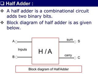
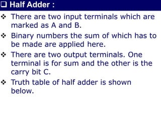
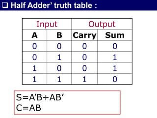
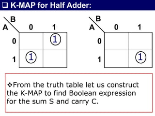
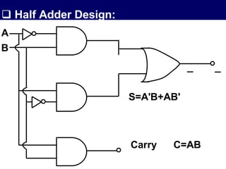
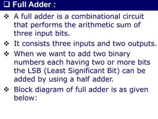
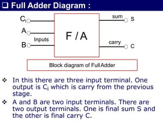
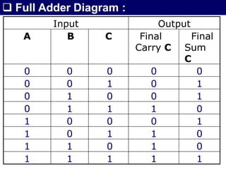
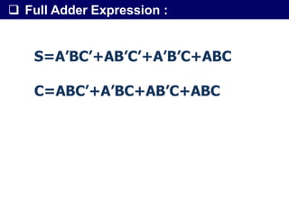
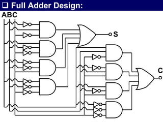
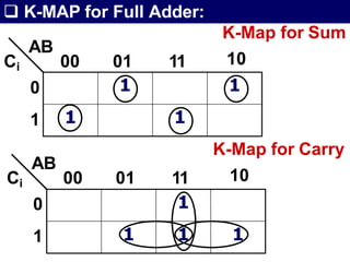
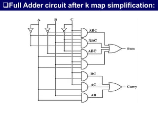
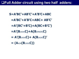
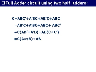
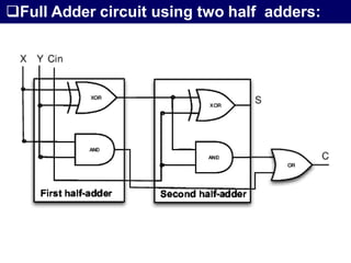
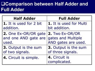
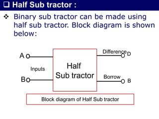
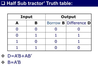
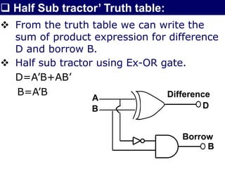
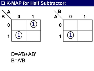
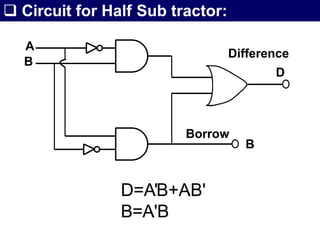
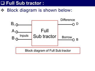
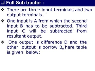
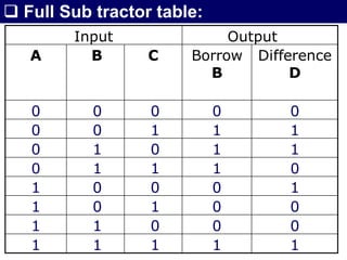
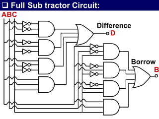
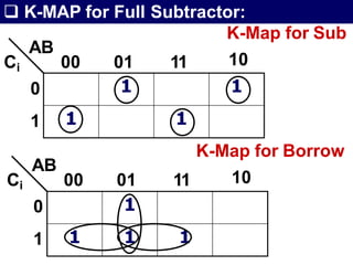
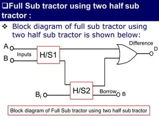
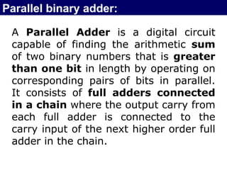
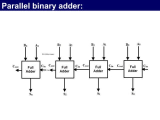
CHAPTER – 7
COMBINATIONAL CIRCUIT
 What is Combinational Circuits? :
 It is logical circuits, the output at any
time depends on the logic levels at the
input at that instant only.
 It does not depend on the past
condition.
 A combinational circuit transforms
binary information from the given
output data to the required output data.
 Half Adder :
 A half adder is a combinational circuit
adds two binary bits.
 Block diagram of half adder is as given
below.
H / A
Inputs
A
B
S
C
sum
carry
Block diagram of HalfAdder
 Half Adder :
 There are two input terminals which are
marked as A and B.
 Binary numbers the sum of which has to
be made are applied here.
 There are two output terminals. One
terminal is for sum and the other is the
carry bit C.
 Truth table of half adder is shown
below.
 Half Adder’ truth table :
Input Output
A B Carry Sum
0 0 0 0
0 1 0 1
1 0 0 1
1 1 1 0
S=A’B+AB’
C=AB
 K-MAP for Half Adder:
1
1
B
A
0
1
0 1
1
B
A
0
1
0 1
From the truth table let us construct
the K-MAP to find Boolean expression
for the sum S and carry C.
Carry C=AB
 Half Adder Design:
A
B
S=A'B+AB'
 Full Adder :
 A full adder is a combinational circuit
that performs the arithmetic sum of
three input bits.
 It consists three inputs and two outputs.
 When we want to add two binary
numbers each having two or more bits
the LSB (Least Significant Bit) can be
added by using a half adder.
 Block diagram of full adder is as given
below:
 Full Adder Diagram :
F / A
Inputs
S
C
sum
carry
Block diagram of FullAdder
Ci
A
B
 In this there are three input terminal. One
output is Ci which is carry from the previous
stage.
 A and B are two input terminals. There are
two output terminals. One is final sum S and
the other is final carry C.
 Full Adder Diagram :
Input Output
A B C Final
Carry C
Final
Sum
C
0 0 0 0 0
0 0 1 0 1
0 1 0 0 1
0 1 1 1 0
1 0 0 0 1
1 0 1 1 0
1 1 0 1 0
1 1 1 1 1
S=A’BC’+AB’C’+A’B’C+ABC
C=ABC’+A’BC+AB’C+ABC
 Full Adder Expression :
 Full Adder Design:
ABC
S
C
 K-MAP for Full Adder:
AB
0
1
1 1
1 1
Ci 00 01 11
K-Map for Sum
10
Ci
AB
0
1
00 01
1
1 1 1
11
K-Map for Carry
10
Full Adder circuit after k map simplification:
Full Adder circuit using two half adders:
S=A’BC’+AB’C’+A’B’C+ABC
=A’BC’+A’B’C+ABC+ AB’C’
=A’(BC’+B’C)+A(BC+B’C’)
=A’(B(XOR)C)+A(B(XNOR)C)
= A’(B(XOR)C)+ A(B(XOR)C)’
= (AXOR(B(XOR)C))
Full Adder circuit using two half adders:
C=ABC’+A’BC+AB’C+ABC
=AB’C+A’BC+ABC+ ABC’
=C(AB’+A’B)+AB(C+C’)
=C(AXORB)+AB
Full Adder circuit using two half adders:
Comparison between Half Adder and
Full Adder
Half Adder Full Adder
1. It is used for 2 bit
addition.
1. It is used for Multi
bit addition.
2. One Ex-OR/OR gate
and one AND gate are
used.
2. Two Ex-OR/OR
gates and Multiple
AND gates are used.
3. Output is the sum
of two signals.
3. Output is the sum
of three signals.
4. Circuit is simple. 4. Circuit is
complicated.
 Half Sub tractor :
 Binary sub tractor can be made using
half sub tractor. Block diagram is shown
below:
Half
Sub tractor
Inputs
A
B
DifferenceD
B
Borrow
Block diagram of Half Sub tractor
 Half Sub tractor :
 There are two input terminals A and B
bits to be subtracted are applied here.
 There are two output terminals. One is
for the difference signal and the other is
for borrow signal. Truth table is as given
below:
 Half Sub tractor’ Truth table:
Input Output
A B Borrow B Difference D
0 0 0 0
0 1 1 1
1 0 0 1
1 1 0 0
 D=A’B+AB’
 B=A’B
 Half Sub tractor’ Truth table:
 From the truth table we can write the
sum of product expression for difference
D and borrow B.
 Half sub tractor using Ex-OR gate.
D=A’B+AB’
B=A’B
A
B
Borrow
B
Difference
D
 K-MAP for Half Subtractor:
1
1
A
B
0
1
0 1
1
B
A
0
1
0 1
D=A'B+AB'
B=A'B
 Circuit for Half Sub tractor:
A
B
B
Borrow
Difference
D
D=A'B+AB'
B=A'B
 Full Sub tractor :
 Block diagram is shown below:
Full
Sub tractor
Inputs
Bi
A
B
D
B
Difference
Borrow
Block diagram of Full Sub tractor
 Full Sub tractor :
 There are three input terminals and two
output terminals.
 One input is A from which the second
input B has to be subtracted. Third
input C will be subtracted from
resultant output.
 One output is difference D and the
other output is borrow Bo here table
is given below:
 Full Sub tractor table:
Input Output
A B C Borrow
B
Difference
D
0 0 0 0 0
0 0 1 1 1
0 1 0 1 1
0 1 1 1 0
1 0 0 0 1
1 0 1 0 0
1 1 0 0 0
1 1 1 1 1
 Full Sub tractor Circuit:
ABC
Difference
D
Borrow
B
 K-MAP for Full Subtractor:
AB
0
1
1 1
1 1
Ci 00 01 11
K-Map for Sub
10
Ci
AB
0
1
00 01
1
1 1 1
11
K-Map for Borrow
10
Full Sub tractor using two half sub
tractor :
 Block diagram of full sub tractor using
two half sub tractor is shown below:
H/S1
Inputs
A
B
D
B
Borrow
Block diagram of Full Sub tractor using two half sub tractor
Bi
H/S2
Difference
D
Parallel binary adder:
A Parallel Adder is a digital circuit
capable of finding the arithmetic sum
of two binary numbers that is greater
than one bit in length by operating on
corresponding pairs of bits in parallel.
It consists of full adders connected
in a chain where the output carry from
each full adder is connected to the
carry input of the next higher order full
adder in the chain.
Parallel binary adder:

combinational circuit-Half Adder ,full Adder

  • 1.
  • 2.
     What isCombinational Circuits? :  It is logical circuits, the output at any time depends on the logic levels at the input at that instant only.  It does not depend on the past condition.  A combinational circuit transforms binary information from the given output data to the required output data.
  • 3.
     Half Adder:  A half adder is a combinational circuit adds two binary bits.  Block diagram of half adder is as given below. H / A Inputs A B S C sum carry Block diagram of HalfAdder
  • 4.
     Half Adder:  There are two input terminals which are marked as A and B.  Binary numbers the sum of which has to be made are applied here.  There are two output terminals. One terminal is for sum and the other is the carry bit C.  Truth table of half adder is shown below.
  • 5.
     Half Adder’truth table : Input Output A B Carry Sum 0 0 0 0 0 1 0 1 1 0 0 1 1 1 1 0 S=A’B+AB’ C=AB
  • 6.
     K-MAP forHalf Adder: 1 1 B A 0 1 0 1 1 B A 0 1 0 1 From the truth table let us construct the K-MAP to find Boolean expression for the sum S and carry C.
  • 7.
    Carry C=AB  HalfAdder Design: A B S=A'B+AB'
  • 8.
     Full Adder:  A full adder is a combinational circuit that performs the arithmetic sum of three input bits.  It consists three inputs and two outputs.  When we want to add two binary numbers each having two or more bits the LSB (Least Significant Bit) can be added by using a half adder.  Block diagram of full adder is as given below:
  • 9.
     Full AdderDiagram : F / A Inputs S C sum carry Block diagram of FullAdder Ci A B  In this there are three input terminal. One output is Ci which is carry from the previous stage.  A and B are two input terminals. There are two output terminals. One is final sum S and the other is final carry C.
  • 10.
     Full AdderDiagram : Input Output A B C Final Carry C Final Sum C 0 0 0 0 0 0 0 1 0 1 0 1 0 0 1 0 1 1 1 0 1 0 0 0 1 1 0 1 1 0 1 1 0 1 0 1 1 1 1 1
  • 11.
  • 12.
     Full AdderDesign: ABC S C
  • 13.
     K-MAP forFull Adder: AB 0 1 1 1 1 1 Ci 00 01 11 K-Map for Sum 10 Ci AB 0 1 00 01 1 1 1 1 11 K-Map for Carry 10
  • 14.
    Full Adder circuitafter k map simplification:
  • 15.
    Full Adder circuitusing two half adders: S=A’BC’+AB’C’+A’B’C+ABC =A’BC’+A’B’C+ABC+ AB’C’ =A’(BC’+B’C)+A(BC+B’C’) =A’(B(XOR)C)+A(B(XNOR)C) = A’(B(XOR)C)+ A(B(XOR)C)’ = (AXOR(B(XOR)C))
  • 16.
    Full Adder circuitusing two half adders: C=ABC’+A’BC+AB’C+ABC =AB’C+A’BC+ABC+ ABC’ =C(AB’+A’B)+AB(C+C’) =C(AXORB)+AB
  • 17.
    Full Adder circuitusing two half adders:
  • 18.
    Comparison between HalfAdder and Full Adder Half Adder Full Adder 1. It is used for 2 bit addition. 1. It is used for Multi bit addition. 2. One Ex-OR/OR gate and one AND gate are used. 2. Two Ex-OR/OR gates and Multiple AND gates are used. 3. Output is the sum of two signals. 3. Output is the sum of three signals. 4. Circuit is simple. 4. Circuit is complicated.
  • 19.
     Half Subtractor :  Binary sub tractor can be made using half sub tractor. Block diagram is shown below: Half Sub tractor Inputs A B DifferenceD B Borrow Block diagram of Half Sub tractor
  • 20.
     Half Subtractor :  There are two input terminals A and B bits to be subtracted are applied here.  There are two output terminals. One is for the difference signal and the other is for borrow signal. Truth table is as given below:
  • 21.
     Half Subtractor’ Truth table: Input Output A B Borrow B Difference D 0 0 0 0 0 1 1 1 1 0 0 1 1 1 0 0  D=A’B+AB’  B=A’B
  • 22.
     Half Subtractor’ Truth table:  From the truth table we can write the sum of product expression for difference D and borrow B.  Half sub tractor using Ex-OR gate. D=A’B+AB’ B=A’B A B Borrow B Difference D
  • 23.
     K-MAP forHalf Subtractor: 1 1 A B 0 1 0 1 1 B A 0 1 0 1 D=A'B+AB' B=A'B
  • 24.
     Circuit forHalf Sub tractor: A B B Borrow Difference D D=A'B+AB' B=A'B
  • 25.
     Full Subtractor :  Block diagram is shown below: Full Sub tractor Inputs Bi A B D B Difference Borrow Block diagram of Full Sub tractor
  • 26.
     Full Subtractor :  There are three input terminals and two output terminals.  One input is A from which the second input B has to be subtracted. Third input C will be subtracted from resultant output.  One output is difference D and the other output is borrow Bo here table is given below:
  • 27.
     Full Subtractor table: Input Output A B C Borrow B Difference D 0 0 0 0 0 0 0 1 1 1 0 1 0 1 1 0 1 1 1 0 1 0 0 0 1 1 0 1 0 0 1 1 0 0 0 1 1 1 1 1
  • 28.
     Full Subtractor Circuit: ABC Difference D Borrow B
  • 29.
     K-MAP forFull Subtractor: AB 0 1 1 1 1 1 Ci 00 01 11 K-Map for Sub 10 Ci AB 0 1 00 01 1 1 1 1 11 K-Map for Borrow 10
  • 30.
    Full Sub tractorusing two half sub tractor :  Block diagram of full sub tractor using two half sub tractor is shown below: H/S1 Inputs A B D B Borrow Block diagram of Full Sub tractor using two half sub tractor Bi H/S2 Difference D
  • 31.
    Parallel binary adder: AParallel Adder is a digital circuit capable of finding the arithmetic sum of two binary numbers that is greater than one bit in length by operating on corresponding pairs of bits in parallel. It consists of full adders connected in a chain where the output carry from each full adder is connected to the carry input of the next higher order full adder in the chain.
  • 32.