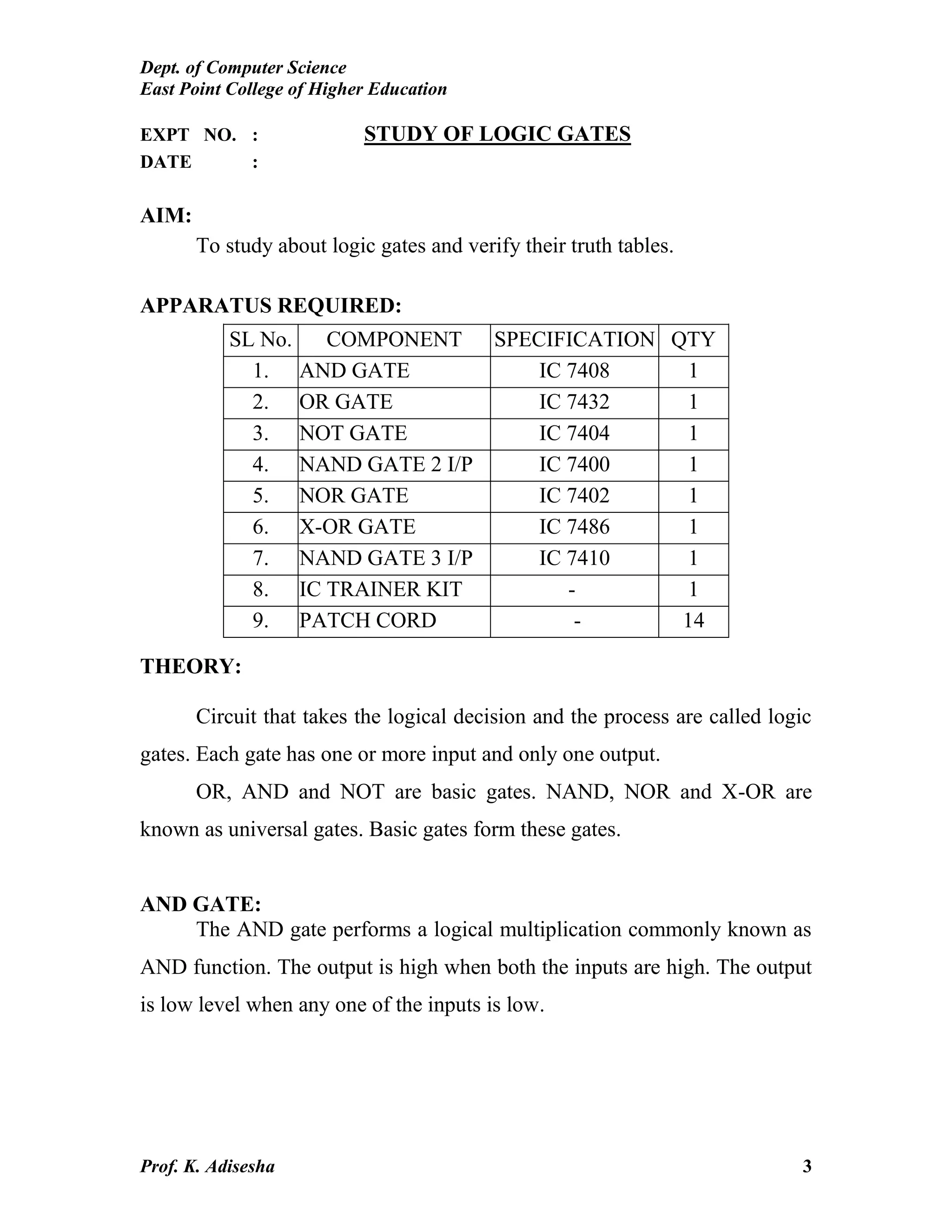
Dept. of Computer Science
East Point College of Higher Education
Prof. K. Adisesha 1
(DIGITAL ELECTRONICS )
LAB MANUAL
LIST OF EXPERIMENTS
1. Study of logic gates.
2. Design and implementation of Basic gates using universal gates
3. Design and implementation of adders and subtractors using logic
gates.
4. Design and implementation of adders and subtractors using
universal gates.
5. Design and implementation of Full adders and subtractors using
logic gates
6. Design and implementation of 4-bit binary adder using IC 7483.
7. Design and implementation of 4-bit binary adder/subtractor
using IC 7483.
8. Design and implementation of 4-bit binary BCD adder using IC
7483.
9. Design and implementation of code converters using logic gates.
10. Implementation of SISO, SIPO, PISO and PIPO shift
registers using flip-flops.
Dept. of Computer Science
East Point College of Higher Education
Prof. K. Adisesha 2
INDEX
XP.
NO
DATE NAME OF THE EXPERIMENT PAGE
NO
MARKS SIGNATURE
Dept. of Computer Science
East Point College of Higher Education
Prof. K. Adisesha 3
EXPT NO. : STUDY OF LOGIC GATES
DATE :
AIM:
To study about logic gates and verify their truth tables.
APPARATUS REQUIRED:
THEORY:
Circuit that takes the logical decision and the process are called logic
gates. Each gate has one or more input and only one output.
OR, AND and NOT are basic gates. NAND, NOR and X-OR are
known as universal gates. Basic gates form these gates.
AND GATE:
The AND gate performs a logical multiplication commonly known as
AND function. The output is high when both the inputs are high. The output
is low level when any one of the inputs is low.
SL No. COMPONENT SPECIFICATION QTY
1. AND GATE IC 7408 1
2. OR GATE IC 7432 1
3. NOT GATE IC 7404 1
4. NAND GATE 2 I/P IC 7400 1
5. NOR GATE IC 7402 1
6. X-OR GATE IC 7486 1
7. NAND GATE 3 I/P IC 7410 1
8. IC TRAINER KIT - 1
9. PATCH CORD - 14
Dept. of Computer Science
East Point College of Higher Education
Prof. K. Adisesha 4
OR GATE:
The OR gate performs a logical addition commonly known as OR
function. The output is high when any one of the inputs is high. The output
is low level when both the inputs are low.
NOT GATE:
The NOT gate is called an inverter. The output is high when the
input is low. The output is low when the input is high.
NAND GATE:
The NAND gate is a contraction of AND-NOT. The output is high
when both inputs are low and any one of the input is low .The output is low
level when both inputs are high.
NOR GATE:
The NOR gate is a contraction of OR-NOT. The output is high when
both inputs are low. The output is low when one or both inputs are high.
X-OR GATE:
The output is high when any one of the inputs is high. The output is
low when both the inputs are low and both the inputs are high.
PROCEDURE:
(i) Connections are given as per circuit diagram.
(ii) Logical inputs are given as per circuit diagram.
(iii) Observe the output and verify the truth table.
Dept. of Computer Science
East Point College of Higher Education
Prof. K. Adisesha 5
AND GATE:
SYMBOL: PIN DIAGRAM:
OR GATE:
Dept. of Computer Science
East Point College of Higher Education
Prof. K. Adisesha 6
NOT GATE:
SYMBOL: PIN DIAGRAM:
X-OR GATE :
SYMBOL : PIN DIAGRAM :
Dept. of Computer Science
East Point College of Higher Education
Prof. K. Adisesha 7
2-INPUT NAND GATE:
SYMBOL: PIN DIAGRAM:
3-INPUT NAND GATE :
Dept. of Computer Science
East Point College of Higher Education
Prof. K. Adisesha 8
NOR GATE:
RESULT:
Dept. of Computer Science
East Point College of Higher Education
Prof. K. Adisesha 9
EXPT NO. : STUDY OF UNIVERSAL GATES
DATE :
AIM:
To study about Universal gates and verify their truth tables.
APPARATUS REQUIRED:
THEORY:
Universal gates are the ones which can be used for implementing any gate
like AND, OR and NOT, or any combination of these basic gates; NAND
and NOR gates are universal gates.
NAND GATE:
Any logic function can be implemented using NAND gates. To
achieve this, first the logic function has to be written in Sum of Product
(SOP) form. Once logic function is converted to SOP, then is very easy to
implement using NAND gate.
NOR GATE:
Any logic function can be implemented using NOR gates. To achieve this,
first the logic function has to be written in Product of Sum (POS) form.
Once it is converted to POS, then it's very easy to implement using NOR
gate.
SL No. COMPONENT SPECIFICATION QTY
1. NAND GATE 2 I/P IC 7400 1
2. NOR GATE IC 7402 1
3. IC TRAINER KIT - 1
4. PATCH CORD - 14
Dept. of Computer Science
East Point College of Higher Education
Prof. K. Adisesha 10
NAND as Universal Gates
NOR as Universal Gate
Result:
Dept. of Computer Science
East Point College of Higher Education
Prof. K. Adisesha 11
EXPT NO. : DESIGN OF HALF ADDER AND SUBTRACTOR
USING LOGIC GATES
DATE :
AIM:
To design and construct half adder, full adder, half subtractor and full
subtractor circuits and verify the truth table using logic gates.
APPARATUS REQUIRED:
Sl.No. COMPONENT SPECIFICATION QTY.
1. AND GATE IC 7408 1
2. X-OR GATE IC 7486 1
3. NOT GATE IC 7404 1
4. OR GATE IC 7432 1
3. IC TRAINER KIT - 1
4. PATCH CORDS - 23
THEORY:
HALF ADDER:
A half adder has two inputs for the two bits to be added and two
outputs one from the sum ‘ S’ and other from the carry ‘ c’ into the higher
adder position. Above circuit is called as a carry signal from the addition of
the less significant bits sum from the X-OR Gate the carry out from the
AND gate.
Dept. of Computer Science
East Point College of Higher Education
Prof. K. Adisesha 12
HALF SUBTRACTOR:
The half subtractor is constructed using X-OR and AND Gate. The
half subtractor has two input and two outputs. The outputs are difference and
borrow. The difference can be applied using X-OR Gate, borrow output can
be implemented using an AND Gate and an inverter.
LOGIC DIAGRAM:
HALF ADDER
TRUTH TABLE:
A B CARRY SUM
0
0
1
1
0
1
0
1
0
0
0
1
0
1
1
0
LOGIC DIAGRAM:
HALF SUBTRACTOR
Dept. of Computer Science
East Point College of Higher Education
Prof. K. Adisesha 13
TRUTH TABLE:
A B BORROW DIFFERENCE
0
0
1
1
0
1
0
1
0
1
0
0
0
1
1
0
PROCEEDURE:
(i) Connections are given as per circuit diagram.
(ii) Logical inputs are given as per circuit diagram.
(iii) Observe the output and verify the truth table.
RESULT:
Dept. of Computer Science
East Point College of Higher Education
Prof. K. Adisesha 14
EXPT NO. : DESIGN OF FULL ADDER USING LOGIC GATES
DATE :
AIM:
To design and construct full adder circuits and verify the truth table
using logic gates.
APPARATUS REQUIRED:
Sl.No. COMPONENT SPECIFICATION QTY.
1. AND GATE IC 7408 1
2. X-OR GATE IC 7486 1
3. NOT GATE IC 7404 1
4. OR GATE IC 7432 1
3. IC TRAINER KIT - 1
4. PATCH CORDS - 23
THEORY:
FULL ADDER:
A full adder is a combinational circuit that forms the arithmetic sum
of input; it consists of three inputs and two outputs. A full adder is useful to
add three bits at a time but a half adder cannot do so. In full adder sum
output will be taken from X-OR Gate, carry output will be taken from OR
Gate.
LOGIC DIAGRAM:
Dept. of Computer Science
East Point College of Higher Education
Prof. K. Adisesha 15
FULL ADDER
FULL ADDER USING TWO HALF ADDER
TRUTH TABLE:
A B C CARRY SUM
0
0
0
0
1
1
1
1
0
0
1
1
0
0
1
1
0
1
0
1
0
1
0
1
0
0
0
1
0
1
1
1
0
1
1
0
1
0
0
1
SUM = A’B’C + A’BC’ + ABC’ + ABC
CARRY = AB + BC + AC
PROCEEDURE:
(iv) Connections are given as per circuit diagram.
(v) Logical inputs are given as per circuit diagram.
(vi) Observe the output and verify the truth table.
RESULT:
Dept. of Computer Science
East Point College of Higher Education
Prof. K. Adisesha 16
EXPT NO. : DESIGN OF FULL SUBTRACTOR USING LOGIC
GATES
DATE :
AIM:
To design and construct full subtractor circuits and verify the truth
table using logic gates.
APPARATUS REQUIRED:
Sl.No. COMPONENT SPECIFICATION QTY.
1. AND GATE IC 7408 1
2. X-OR GATE IC 7486 1
3. NOT GATE IC 7404 1
4. OR GATE IC 7432 1
3. IC TRAINER KIT - 1
4. PATCH CORDS - 23
THEORY:
FULL SUBTRACTOR:
The full subtractor is a combination of X-OR, AND, OR, NOT Gates.
In a full subtractor the logic circuit should have three inputs and two outputs.
The two half subtractor put together gives a full subtractor .The first half
subtractor will be C and A B. The output will be difference output of full
subtractor. The expression AB assembles the borrow output of the half
subtractor and the second term is the inverted difference output of first X-
OR.
Dept. of Computer Science
East Point College of Higher Education
Prof. K. Adisesha 17
LOGIC DIAGRAM:
FULL SUBTRACTOR
FULL SUBTRACTOR USING TWO HALF SUBTRACTOR:
TRUTH TABLE:
A B C BORROW DIFFERENCE
0
0
0
0
1
1
1
1
0
0
1
1
0
0
1
1
0
1
0
1
0
1
0
1
0
1
1
1
0
0
0
1
0
1
1
0
1
0
0
1
Dept. of Computer Science
East Point College of Higher Education
Prof. K. Adisesha 18
Difference = A’B’C + A’BC’ + AB’C’ + ABC
Borrow = A’B + BC + A’C
PROCEEDURE:
(vii) Connections are given as per circuit diagram.
(viii) Logical inputs are given as per circuit diagram.
(ix) Observe the output and verify the truth table.
RESULT:
Dept. of Computer Science
East Point College of Higher Education
Prof. K. Adisesha 19
EXPT NO. : DESIGN OF 4-BIT ADDER USING IC 7483
DATE :
AIM:
To design and implement 4-bit adder and subtractor using IC 7483.
APPARATUS REQUIRED:
Sl.No. COMPONENT SPECIFICATION QTY.
1. IC IC 7483 1
2. EX-OR GATE IC 7486 1
3. NOT GATE IC 7404 1
3. IC TRAINER KIT - 1
4. PATCH CORDS - 40
THEORY:
4 BIT BINARY ADDER:
A binary adder is a digital circuit that produces the arithmetic sum of
two binary numbers. It can be constructed with full adders connected in
cascade, with the output carry from each full adder connected to the input
carry of next full adder in chain. The augends bits of ‘A’ and the addend bits
of ‘B’ are designated by subscript numbers from right to left, with subscript
0 denoting the least significant bits. The carries are connected in chain
through the full adder. The input carry to the adder is C0 and it ripples
through the full adder to the output carry C4.
PIN DIAGRAM FOR IC 7483:
Dept. of Computer Science
East Point College of Higher Education
Prof. K. Adisesha 20
LOGIC DIAGRAM:
4-BIT BINARY ADDER
Dept. of Computer Science
East Point College of Higher Education
Prof. K. Adisesha 21
TRUTH TABLE:
PROCEEDURE:
(x) Connections are given as per circuit diagram.
(xi) Logical inputs are given as per circuit diagram.
(xii) Observe the output and verify the truth table.
RESULT:
Input Data A Input Data B Addition
A4 A3 A2 A1 B4 B3 B2 B1 C S4 S3 S2 S1
1 0 0 0 0 0 1 0 0 1 0 1 0
1 0 0 0 1 0 0 0 1 0 0 0 0
0 0 1 0 1 0 0 0 0 1 0 1 0
0 0 0 1 0 1 1 1 0 1 0 0 0
1 0 1 0 1 0 1 1 1 0 0 1 0
1 1 1 0 1 1 1 1 1 1 0 1 0
1 0 1 0 1 1 0 1 1 0 1 1 1
Dept. of Computer Science
East Point College of Higher Education
Prof. K. Adisesha 22
EXPT NO. : DESIGN OF 4-BIT ADDER AND SUBTRACTOR
DATE :
AIM:
To design and implement 4-bit adder and subtractor using IC 7483.
APPARATUS REQUIRED:
Sl.No. COMPONENT SPECIFICATION QTY.
1. IC IC 7483 1
2. EX-OR GATE IC 7486 1
3. NOT GATE IC 7404 1
3. IC TRAINER KIT - 1
4. PATCH CORDS - 40
THEORY:
4 BIT BINARY ADDER:
A binary adder is a digital circuit that produces the arithmetic sum of
two binary numbers. It can be constructed with full adders connected in
cascade, with the output carry from each full adder connected to the input
carry of next full adder in chain. The augends bits of ‘A’ and the addend bits
of ‘B’ are designated by subscript numbers from right to left, with subscript
0 denoting the least significant bits. The carries are connected in chain
through the full adder. The input carry to the adder is C0 and it ripples
through the full adder to the output carry C4.
4 BIT BINARY SUBTRACTOR:
The circuit for subtracting A-B consists of an adder with inverters,
placed between each data input ‘B’ and the corresponding input of full
adder. The input carry C0 must be equal to 1 when performing subtraction.
Dept. of Computer Science
East Point College of Higher Education
Prof. K. Adisesha 23
PIN DIAGRAM FOR IC 7483:
LOGIC DIAGRAM:
4-BIT BINARY ADDER/ SUBTRACTOR
Dept. of Computer Science
East Point College of Higher Education
Prof. K. Adisesha 24
TRUTH TABLE:
PROCEDURE:
(i) Connections were given as per circuit diagram.
(ii) Logical inputs were given as per truth table
(iii) Observe the logical output and verify with the truth tables.
RESULT:
Input Data A Input Data B Addition Subtraction
A4 A3 A2 A1 B4 B3 B2 B1 C S4 S3 S2 S1 B D4 D3 D2 D1
1 0 0 0 0 0 1 0 0 1 0 1 0 1 0 1 1 0
1 0 0 0 1 0 0 0 1 0 0 0 0 1 0 0 0 0
0 0 1 0 1 0 0 0 0 1 0 1 0 0 1 0 1 0
0 0 0 1 0 1 1 1 0 1 0 0 0 0 1 0 1 0
1 0 1 0 1 0 1 1 1 0 0 1 0 0 1 1 1 1
1 1 1 0 1 1 1 1 1 1 0 1 0 0 1 1 1 1
1 0 1 0 1 1 0 1 1 0 1 1 1 0 1 1 0 1
Dept. of Computer Science
East Point College of Higher Education
Prof. K. Adisesha 25
EXPT NO. : DESIGN OF 4-BIT BCD ADDER
DATE :
AIM:
To design and implement 4-bit BCD adder using IC 7483.
APPARATUS REQUIRED:
Sl.No. COMPONENT SPECIFICATION QTY.
1. IC IC 7483 1
2. EX-OR GATE IC 7486 1
3. NOT GATE IC 7404 1
3. IC TRAINER KIT - 1
4. PATCH CORDS - 40
THEORY:
4 BIT BCD ADDER:
Consider the arithmetic addition of two decimal digits in BCD,
together with an input carry from a previous stage. Since each input digit
does not exceed 9, the output sum cannot be greater than 19, the 1 in the sum
being an input carry. The output of two decimal digits must be represented
in BCD and should appear in the form listed in the columns.
ABCD adder that adds 2 BCD digits and produce a sum digit in BCD.
The 2 decimal digits, together with the input carry, are first added in the top
4 bit adder to produce the binary sum.
PIN DIAGRAM FOR IC 7483:
Dept. of Computer Science
East Point College of Higher Education
Prof. K. Adisesha 26
LOGIC DIAGRAM:
BCD ADDER
Y = S4 (S3 + S2)
Dept. of Computer Science
East Point College of Higher Education
Prof. K. Adisesha 27
TRUTH TABLE:
BCD SUM CARRY
S4 S3 S2 S1 C
0 0 0 0 0
0 0 0 1 0
0 0 1 0 0
0 0 1 1 0
0 1 0 0 0
0 1 0 1 0
0 1 1 0 0
0 1 1 1 0
1 0 0 0 0
1 0 0 1 0
1 0 1 0 1
1 0 1 1 1
1 1 0 0 1
1 1 0 1 1
1 1 1 0 1
1 1 1 1 1
PROCEDURE:
(iv) Connections were given as per circuit diagram.
(v) Logical inputs were given as per truth table
(vi) Observe the logical output and verify with the truth tables.
RESULT:
Dept. of Computer Science
East Point College of Higher Education
Prof. K. Adisesha 28
EXPT NO. :
DATE :
DESIGN AND IMPLEMENTATION OF CODE CONVERTOR
AIM:
To design and implement 4-bit
(i) Binary to gray code converter
(ii) Gray to binary code converter
APPARATUS REQUIRED:
Sl.No. COMPONENT SPECIFICATION QTY.
1. X-OR GATE IC 7486 1
2. AND GATE IC 7408 1
3. OR GATE IC 7432 1
4. NOT GATE IC 7404 1
5. IC TRAINER KIT - 1
6. PATCH CORDS - 35
THEORY:
The availability of large variety of codes for the same discrete
elements of information results in the use of different codes by different
systems. A conversion circuit must be inserted between the two systems if
each uses different codes for same information. Thus, code converter is a
circuit that makes the two systems compatible even though each uses
different binary code.
The bit combination assigned to binary code to gray code. Since each
code uses four bits to represent a decimal digit. There are four inputs and
four outputs. Gray code is a non-weighted code.
Dept. of Computer Science
East Point College of Higher Education
Prof. K. Adisesha 29
The input variable are designated as B3, B2, B1, B0 and the output
variables are designated as C3, C2, C1, Co. from the truth table,
combinational circuit is designed. The Boolean functions are obtained from
K-Map for each output variable.
LOGIC DIAGRAM:
BINARY TO GRAY CODE CONVERTOR
Expression for Gray code:
G3 = B3
TRUTH TABLE:
| Binary input | Gray code output |
B3 B2 B1 B0 G3 G2 G1 G0
0
0
0
0
0
0
0
0
0
0
0
1
1
1
0
0
1
1
0
0
1
0
1
0
1
0
1
0
0
0
0
0
0
0
0
0
0
0
0
1
1
1
0
0
1
1
1
1
0
0
1
1
0
0
1
1
Dept. of Computer Science
East Point College of Higher Education
Prof. K. Adisesha 30
0
1
1
1
1
1
1
1
1
1
0
0
0
0
1
1
1
1
1
0
0
1
1
0
0
1
1
1
0
1
0
1
0
1
0
1
0
1
1
1
1
1
1
1
1
1
1
1
1
1
0
0
0
0
0
0
0
1
1
1
1
0
0
0
0
1
1
0
0
1
1
0
LOGIC DIAGRAM:
GRAY CODE TO BINARY CONVERTOR
Expression for Binary code:
B3 = G3
TRUTH TABLE:
|
Dept. of Computer Science
East Point College of Higher Education
Prof. K. Adisesha 31
Gray Code | Binary Code |
G3 G2 G1 G0 B3 B2 B1 B0
0
0
0
0
0
0
0
0
1
1
1
1
1
1
1
1
0
0
0
0
1
1
1
1
1
1
1
1
0
0
0
0
0
0
1
1
1
1
0
0
0
0
1
1
1
1
0
0
0
1
1
0
0
1
1
0
0
1
1
0
0
1
1
0
0
0
0
0
0
0
0
0
1
1
1
1
1
1
1
1
0
0
0
0
1
1
1
1
0
0
0
0
1
1
1
1
0
0
1
1
0
0
1
1
0
0
1
1
0
0
1
1
0
1
0
1
0
1
0
1
0
1
0
1
0
1
0
1
PROCEDURE:
(i) Connections were given as per circuit diagram.
(ii) Logical inputs were given as per truth table
(iii) Observe the logical output and verify with the truth tables.
RESULT:
Dept. of Computer Science
East Point College of Higher Education
Prof. K. Adisesha 32
EXPT NO. :
DATE :
16 BIT ODD/EVEN PARITY CHECKER /GENERATOR
AIM:
To design and implement 16 bit odd/even parity checker generator
using IC 74180.
APPARATUS REQUIRED:
Sl.No. COMPONENT SPECIFICATION QTY.
1. NOT GATE IC 7404 1
1. IC 74180 2
2. IC TRAINER KIT - 1
3. PATCH CORDS - 30
THEORY:
A parity bit is used for detecting errors during transmission of binary
information. A parity bit is an extra bit included with a binary message to
make the number is either even or odd. The message including the parity bit
is transmitted and then checked at the receiver ends for errors. An error is
detected if the checked parity bit doesn’t correspond to the one transmitted.
The circuit that generates the parity bit in the transmitter is called a ‘parity
generator’ and the circuit that checks the parity in the receiver is called a
‘parity checker’.
In even parity, the added parity bit will make the total number is even
amount. In odd parity, the added parity bit will make the total number is odd
Dept. of Computer Science
East Point College of Higher Education
Prof. K. Adisesha 33
amount. The parity checker circuit checks for possible errors in the
transmission. If the information is passed in even parity, then the bits
required must have an even number of 1’s. An error occur during
transmission, if the received bits have an odd number of 1’s indicating that
one bit has changed in value during transmission.
PIN DIAGRAM FOR IC 74180:
FUNCTION TABLE:
INPUTS OUTPUTS
Number of High Data
Inputs (I0 – I7)
PE PO ∑E ∑O
EVEN 1 0 1 0
ODD 1 0 0 1
EVEN 0 1 0 1
ODD 0 1 1 0
X 1 1 0 0
X 0 0 1 1
Dept. of Computer Science
East Point College of Higher Education
Prof. K. Adisesha 34
PROCEDURE:
(i) Connections are given as per circuit diagram.
(ii) Logical inputs are given as per circuit diagram.
(iii) Observe the output and verify the truth table.
RESULT:
Dept. of Computer Science
East Point College of Higher Education
Prof. K. Adisesha 35
EXPT NO. :
DATE :
DESIGN AND IMPLEMENTATION OF MULTIPLEXER AND
DEMULTIPLEXER
AIM:
To design and implement multiplexer and demultiplexer using logic
gates.
APPARATUS REQUIRED:
Sl.No. COMPONENT SPECIFICATION QTY.
1. 3 I/P AND GATE IC 7411 2
2. OR GATE IC 7432 1
3. NOT GATE IC 7404 1
2. IC TRAINER KIT - 1
3. PATCH CORDS - 32
THEORY:
MULTIPLEXER:
Multiplexer means transmitting a large number of information units
over a smaller number of channels or lines. A digital multiplexer is a
combinational circuit that selects binary information from one of many input
lines and directs it to a single output line. The selection of a particular input
line is controlled by a set of selection lines. Normally there are 2n
input line
and n selection lines whose bit combination determine which input is
selected.
DEMULTIPLEXER:
The function of Demultiplexer is in contrast to multiplexer function. It
takes information from one line and distributes it to a given number of
Dept. of Computer Science
East Point College of Higher Education
Prof. K. Adisesha 36
output lines. For this reason, the demultiplexer is also known as a data
distributor. Decoder can also be used as demultiplexer.
In the 1: 4 demultiplexer circuit, the data input line goes to all of the
AND gates. The data select lines enable only one gate at a time and the data
on the data input line will pass through the selected gate to the associated
data output line.
BLOCK DIAGRAM FOR 4:1 MULTIPLEXER:
FUNCTION TABLE:
S1 S0 INPUTS Y
0 0 D0 → D0 S1’ S0’
0 1 D1 → D1 S1’ S0
1 0 D2 → D2 S1 S0’
1 1 D3 → D3 S1 S0
Y = D0 S1’ S0’ + D1 S1’ S0 + D2 S1 S0’ + D3 S1 S0
Dept. of Computer Science
East Point College of Higher Education
Prof. K. Adisesha 37
CIRCUIT DIAGRAM FOR MULTIPLEXER:
TRUTH TABLE:
S1 S0 Y = OUTPUT
0 0 D0
0 1 D1
1 0 D2
1 1 D3
Dept. of Computer Science
East Point College of Higher Education
Prof. K. Adisesha 38
BLOCK DIAGRAM FOR 1:4 DEMULTIPLEXER:
FUNCTION TABLE:
S1 S0 INPUT
0 0 X → D0 = X S1’ S0’
0 1 X → D1 = X S1’ S0
1 0 X → D2 = X S1 S0’
1 1 X → D3 = X S1 S0
Y = X S1’ S0’ + X S1’ S0 + X S1 S0’ + X S1 S0
LOGIC DIAGRAM FOR DEMULTIPLEXER:
Dept. of Computer Science
East Point College of Higher Education
Prof. K. Adisesha 39
TRUTH TABLE:
INPUT OUTPUT
S1 S0 I/P D0 D1 D2 D3
0 0 0 0 0 0 0
0 0 1 1 0 0 0
0 1 0 0 0 0 0
0 1 1 0 1 0 0
1 0 0 0 0 0 0
Dept. of Computer Science
East Point College of Higher Education
Prof. K. Adisesha 40
1 0 1 0 0 1 0
1 1 0 0 0 0 0
1 1 1 0 0 0 1
PROCEDURE:
(i) Connections are given as per circuit diagram.
(ii) Logical inputs are given as per circuit diagram.
(iii) Observe the output and verify the truth table.
RESULT:
Dept. of Computer Science
East Point College of Higher Education
Prof. K. Adisesha 41
EXPT NO. :
DATE :
DESIGN AND IMPLEMENTATION OF SHIFT REGISTER
AIM:
To design and implement
(i) Serial in serial out
(ii) Serial in parallel out
(iii) Parallel in serial out
(iv) Parallel in parallel out
APPARATUS REQUIRED:
Sl.No. COMPONENT SPECIFICATION QTY.
1. D FLIP FLOP IC 7474 2
2. OR GATE IC 7432 1
3. IC TRAINER KIT - 1
4. PATCH CORDS - 35
THEORY:
A register is capable of shifting its binary information in one or both
directions is known as shift register. The logical configuration of shift
register consist of a D-Flip flop cascaded with output of one flip flop
connected to input of next flip flop. All flip flops receive common clock
pulses which causes the shift in the output of the flip flop. The simplest
possible shift register is one that uses only flip flop. The output of a given
flip flop is connected to the input of next flip flop of the register. Each clock
pulse shifts the content of register one bit position to right.
Dept. of Computer Science
East Point College of Higher Education
Prof. K. Adisesha 42
PIN DIAGRAM:
LOGIC DIAGRAM:
SERIAL IN SERIAL OUT:
Dept. of Computer Science
East Point College of Higher Education
Prof. K. Adisesha 43
TRUTH TABLE:
CLK Serial in Serial out
1 1 0
2 0 0
3 0 0
4 1 1
5 X 0
6 X 0
7 X 1
LOGIC DIAGRAM:
SERIAL IN PARALLEL OUT:
TRUTH TABLE:
CLK DATA
OUTPUT
QA QB QC QD
1 1 1 0 0 0
2 0 0 1 0 0
3 0 0 0 1 1
4 1 1 0 0 1
Dept. of Computer Science
East Point College of Higher Education
Prof. K. Adisesha 44
LOGIC DIAGRAM:
PARALLEL IN SERIAL OUT:
TRUTH TABLE:
CLK Q3 Q2 Q1 Q0 O/P
0 1 0 0 1 1
1 0 0 0 0 0
2 0 0 0 0 0
3 0 0 0 0 1
LOGIC DIAGRAM:
PARALLEL IN PARALLEL OUT:
Dept. of Computer Science
East Point College of Higher Education
Prof. K. Adisesha 45
TRUTH TABLE:
CLK
DATA INPUT OUTPUT
DA DB DC DD QA QB QC QD
1 1 0 0 1 1 0 0 1
2 1 0 1 0 1 0 1 0
PROCEDURE:
(i) Connections are given as per circuit diagram.
(ii) Logical inputs are given as per circuit diagram.
(iii) Observe the output and verify the truth table.
RESULT:

DIGITAL ELECTRONICS LAB

  • 1.
    Dept. of ComputerScience East Point College of Higher Education Prof. K. Adisesha 1 (DIGITAL ELECTRONICS ) LAB MANUAL LIST OF EXPERIMENTS 1. Study of logic gates. 2. Design and implementation of Basic gates using universal gates 3. Design and implementation of adders and subtractors using logic gates. 4. Design and implementation of adders and subtractors using universal gates. 5. Design and implementation of Full adders and subtractors using logic gates 6. Design and implementation of 4-bit binary adder using IC 7483. 7. Design and implementation of 4-bit binary adder/subtractor using IC 7483. 8. Design and implementation of 4-bit binary BCD adder using IC 7483. 9. Design and implementation of code converters using logic gates. 10. Implementation of SISO, SIPO, PISO and PIPO shift registers using flip-flops.
  • 2.
    Dept. of ComputerScience East Point College of Higher Education Prof. K. Adisesha 2 INDEX XP. NO DATE NAME OF THE EXPERIMENT PAGE NO MARKS SIGNATURE
  • 3.
    Dept. of ComputerScience East Point College of Higher Education Prof. K. Adisesha 3 EXPT NO. : STUDY OF LOGIC GATES DATE : AIM: To study about logic gates and verify their truth tables. APPARATUS REQUIRED: THEORY: Circuit that takes the logical decision and the process are called logic gates. Each gate has one or more input and only one output. OR, AND and NOT are basic gates. NAND, NOR and X-OR are known as universal gates. Basic gates form these gates. AND GATE: The AND gate performs a logical multiplication commonly known as AND function. The output is high when both the inputs are high. The output is low level when any one of the inputs is low. SL No. COMPONENT SPECIFICATION QTY 1. AND GATE IC 7408 1 2. OR GATE IC 7432 1 3. NOT GATE IC 7404 1 4. NAND GATE 2 I/P IC 7400 1 5. NOR GATE IC 7402 1 6. X-OR GATE IC 7486 1 7. NAND GATE 3 I/P IC 7410 1 8. IC TRAINER KIT - 1 9. PATCH CORD - 14
  • 4.
    Dept. of ComputerScience East Point College of Higher Education Prof. K. Adisesha 4 OR GATE: The OR gate performs a logical addition commonly known as OR function. The output is high when any one of the inputs is high. The output is low level when both the inputs are low. NOT GATE: The NOT gate is called an inverter. The output is high when the input is low. The output is low when the input is high. NAND GATE: The NAND gate is a contraction of AND-NOT. The output is high when both inputs are low and any one of the input is low .The output is low level when both inputs are high. NOR GATE: The NOR gate is a contraction of OR-NOT. The output is high when both inputs are low. The output is low when one or both inputs are high. X-OR GATE: The output is high when any one of the inputs is high. The output is low when both the inputs are low and both the inputs are high. PROCEDURE: (i) Connections are given as per circuit diagram. (ii) Logical inputs are given as per circuit diagram. (iii) Observe the output and verify the truth table.
  • 5.
    Dept. of ComputerScience East Point College of Higher Education Prof. K. Adisesha 5 AND GATE: SYMBOL: PIN DIAGRAM: OR GATE:
  • 6.
    Dept. of ComputerScience East Point College of Higher Education Prof. K. Adisesha 6 NOT GATE: SYMBOL: PIN DIAGRAM: X-OR GATE : SYMBOL : PIN DIAGRAM :
  • 7.
    Dept. of ComputerScience East Point College of Higher Education Prof. K. Adisesha 7 2-INPUT NAND GATE: SYMBOL: PIN DIAGRAM: 3-INPUT NAND GATE :
  • 8.
    Dept. of ComputerScience East Point College of Higher Education Prof. K. Adisesha 8 NOR GATE: RESULT:
  • 9.
    Dept. of ComputerScience East Point College of Higher Education Prof. K. Adisesha 9 EXPT NO. : STUDY OF UNIVERSAL GATES DATE : AIM: To study about Universal gates and verify their truth tables. APPARATUS REQUIRED: THEORY: Universal gates are the ones which can be used for implementing any gate like AND, OR and NOT, or any combination of these basic gates; NAND and NOR gates are universal gates. NAND GATE: Any logic function can be implemented using NAND gates. To achieve this, first the logic function has to be written in Sum of Product (SOP) form. Once logic function is converted to SOP, then is very easy to implement using NAND gate. NOR GATE: Any logic function can be implemented using NOR gates. To achieve this, first the logic function has to be written in Product of Sum (POS) form. Once it is converted to POS, then it's very easy to implement using NOR gate. SL No. COMPONENT SPECIFICATION QTY 1. NAND GATE 2 I/P IC 7400 1 2. NOR GATE IC 7402 1 3. IC TRAINER KIT - 1 4. PATCH CORD - 14
  • 10.
    Dept. of ComputerScience East Point College of Higher Education Prof. K. Adisesha 10 NAND as Universal Gates NOR as Universal Gate Result:
  • 11.
    Dept. of ComputerScience East Point College of Higher Education Prof. K. Adisesha 11 EXPT NO. : DESIGN OF HALF ADDER AND SUBTRACTOR USING LOGIC GATES DATE : AIM: To design and construct half adder, full adder, half subtractor and full subtractor circuits and verify the truth table using logic gates. APPARATUS REQUIRED: Sl.No. COMPONENT SPECIFICATION QTY. 1. AND GATE IC 7408 1 2. X-OR GATE IC 7486 1 3. NOT GATE IC 7404 1 4. OR GATE IC 7432 1 3. IC TRAINER KIT - 1 4. PATCH CORDS - 23 THEORY: HALF ADDER: A half adder has two inputs for the two bits to be added and two outputs one from the sum ‘ S’ and other from the carry ‘ c’ into the higher adder position. Above circuit is called as a carry signal from the addition of the less significant bits sum from the X-OR Gate the carry out from the AND gate.
  • 12.
    Dept. of ComputerScience East Point College of Higher Education Prof. K. Adisesha 12 HALF SUBTRACTOR: The half subtractor is constructed using X-OR and AND Gate. The half subtractor has two input and two outputs. The outputs are difference and borrow. The difference can be applied using X-OR Gate, borrow output can be implemented using an AND Gate and an inverter. LOGIC DIAGRAM: HALF ADDER TRUTH TABLE: A B CARRY SUM 0 0 1 1 0 1 0 1 0 0 0 1 0 1 1 0 LOGIC DIAGRAM: HALF SUBTRACTOR
  • 13.
    Dept. of ComputerScience East Point College of Higher Education Prof. K. Adisesha 13 TRUTH TABLE: A B BORROW DIFFERENCE 0 0 1 1 0 1 0 1 0 1 0 0 0 1 1 0 PROCEEDURE: (i) Connections are given as per circuit diagram. (ii) Logical inputs are given as per circuit diagram. (iii) Observe the output and verify the truth table. RESULT:
  • 14.
    Dept. of ComputerScience East Point College of Higher Education Prof. K. Adisesha 14 EXPT NO. : DESIGN OF FULL ADDER USING LOGIC GATES DATE : AIM: To design and construct full adder circuits and verify the truth table using logic gates. APPARATUS REQUIRED: Sl.No. COMPONENT SPECIFICATION QTY. 1. AND GATE IC 7408 1 2. X-OR GATE IC 7486 1 3. NOT GATE IC 7404 1 4. OR GATE IC 7432 1 3. IC TRAINER KIT - 1 4. PATCH CORDS - 23 THEORY: FULL ADDER: A full adder is a combinational circuit that forms the arithmetic sum of input; it consists of three inputs and two outputs. A full adder is useful to add three bits at a time but a half adder cannot do so. In full adder sum output will be taken from X-OR Gate, carry output will be taken from OR Gate. LOGIC DIAGRAM:
  • 15.
    Dept. of ComputerScience East Point College of Higher Education Prof. K. Adisesha 15 FULL ADDER FULL ADDER USING TWO HALF ADDER TRUTH TABLE: A B C CARRY SUM 0 0 0 0 1 1 1 1 0 0 1 1 0 0 1 1 0 1 0 1 0 1 0 1 0 0 0 1 0 1 1 1 0 1 1 0 1 0 0 1 SUM = A’B’C + A’BC’ + ABC’ + ABC CARRY = AB + BC + AC PROCEEDURE: (iv) Connections are given as per circuit diagram. (v) Logical inputs are given as per circuit diagram. (vi) Observe the output and verify the truth table. RESULT:
  • 16.
    Dept. of ComputerScience East Point College of Higher Education Prof. K. Adisesha 16 EXPT NO. : DESIGN OF FULL SUBTRACTOR USING LOGIC GATES DATE : AIM: To design and construct full subtractor circuits and verify the truth table using logic gates. APPARATUS REQUIRED: Sl.No. COMPONENT SPECIFICATION QTY. 1. AND GATE IC 7408 1 2. X-OR GATE IC 7486 1 3. NOT GATE IC 7404 1 4. OR GATE IC 7432 1 3. IC TRAINER KIT - 1 4. PATCH CORDS - 23 THEORY: FULL SUBTRACTOR: The full subtractor is a combination of X-OR, AND, OR, NOT Gates. In a full subtractor the logic circuit should have three inputs and two outputs. The two half subtractor put together gives a full subtractor .The first half subtractor will be C and A B. The output will be difference output of full subtractor. The expression AB assembles the borrow output of the half subtractor and the second term is the inverted difference output of first X- OR.
  • 17.
    Dept. of ComputerScience East Point College of Higher Education Prof. K. Adisesha 17 LOGIC DIAGRAM: FULL SUBTRACTOR FULL SUBTRACTOR USING TWO HALF SUBTRACTOR: TRUTH TABLE: A B C BORROW DIFFERENCE 0 0 0 0 1 1 1 1 0 0 1 1 0 0 1 1 0 1 0 1 0 1 0 1 0 1 1 1 0 0 0 1 0 1 1 0 1 0 0 1
  • 18.
    Dept. of ComputerScience East Point College of Higher Education Prof. K. Adisesha 18 Difference = A’B’C + A’BC’ + AB’C’ + ABC Borrow = A’B + BC + A’C PROCEEDURE: (vii) Connections are given as per circuit diagram. (viii) Logical inputs are given as per circuit diagram. (ix) Observe the output and verify the truth table. RESULT:
  • 19.
    Dept. of ComputerScience East Point College of Higher Education Prof. K. Adisesha 19 EXPT NO. : DESIGN OF 4-BIT ADDER USING IC 7483 DATE : AIM: To design and implement 4-bit adder and subtractor using IC 7483. APPARATUS REQUIRED: Sl.No. COMPONENT SPECIFICATION QTY. 1. IC IC 7483 1 2. EX-OR GATE IC 7486 1 3. NOT GATE IC 7404 1 3. IC TRAINER KIT - 1 4. PATCH CORDS - 40 THEORY: 4 BIT BINARY ADDER: A binary adder is a digital circuit that produces the arithmetic sum of two binary numbers. It can be constructed with full adders connected in cascade, with the output carry from each full adder connected to the input carry of next full adder in chain. The augends bits of ‘A’ and the addend bits of ‘B’ are designated by subscript numbers from right to left, with subscript 0 denoting the least significant bits. The carries are connected in chain through the full adder. The input carry to the adder is C0 and it ripples through the full adder to the output carry C4. PIN DIAGRAM FOR IC 7483:
  • 20.
    Dept. of ComputerScience East Point College of Higher Education Prof. K. Adisesha 20 LOGIC DIAGRAM: 4-BIT BINARY ADDER
  • 21.
    Dept. of ComputerScience East Point College of Higher Education Prof. K. Adisesha 21 TRUTH TABLE: PROCEEDURE: (x) Connections are given as per circuit diagram. (xi) Logical inputs are given as per circuit diagram. (xii) Observe the output and verify the truth table. RESULT: Input Data A Input Data B Addition A4 A3 A2 A1 B4 B3 B2 B1 C S4 S3 S2 S1 1 0 0 0 0 0 1 0 0 1 0 1 0 1 0 0 0 1 0 0 0 1 0 0 0 0 0 0 1 0 1 0 0 0 0 1 0 1 0 0 0 0 1 0 1 1 1 0 1 0 0 0 1 0 1 0 1 0 1 1 1 0 0 1 0 1 1 1 0 1 1 1 1 1 1 0 1 0 1 0 1 0 1 1 0 1 1 0 1 1 1
  • 22.
    Dept. of ComputerScience East Point College of Higher Education Prof. K. Adisesha 22 EXPT NO. : DESIGN OF 4-BIT ADDER AND SUBTRACTOR DATE : AIM: To design and implement 4-bit adder and subtractor using IC 7483. APPARATUS REQUIRED: Sl.No. COMPONENT SPECIFICATION QTY. 1. IC IC 7483 1 2. EX-OR GATE IC 7486 1 3. NOT GATE IC 7404 1 3. IC TRAINER KIT - 1 4. PATCH CORDS - 40 THEORY: 4 BIT BINARY ADDER: A binary adder is a digital circuit that produces the arithmetic sum of two binary numbers. It can be constructed with full adders connected in cascade, with the output carry from each full adder connected to the input carry of next full adder in chain. The augends bits of ‘A’ and the addend bits of ‘B’ are designated by subscript numbers from right to left, with subscript 0 denoting the least significant bits. The carries are connected in chain through the full adder. The input carry to the adder is C0 and it ripples through the full adder to the output carry C4. 4 BIT BINARY SUBTRACTOR: The circuit for subtracting A-B consists of an adder with inverters, placed between each data input ‘B’ and the corresponding input of full adder. The input carry C0 must be equal to 1 when performing subtraction.
  • 23.
    Dept. of ComputerScience East Point College of Higher Education Prof. K. Adisesha 23 PIN DIAGRAM FOR IC 7483: LOGIC DIAGRAM: 4-BIT BINARY ADDER/ SUBTRACTOR
  • 24.
    Dept. of ComputerScience East Point College of Higher Education Prof. K. Adisesha 24 TRUTH TABLE: PROCEDURE: (i) Connections were given as per circuit diagram. (ii) Logical inputs were given as per truth table (iii) Observe the logical output and verify with the truth tables. RESULT: Input Data A Input Data B Addition Subtraction A4 A3 A2 A1 B4 B3 B2 B1 C S4 S3 S2 S1 B D4 D3 D2 D1 1 0 0 0 0 0 1 0 0 1 0 1 0 1 0 1 1 0 1 0 0 0 1 0 0 0 1 0 0 0 0 1 0 0 0 0 0 0 1 0 1 0 0 0 0 1 0 1 0 0 1 0 1 0 0 0 0 1 0 1 1 1 0 1 0 0 0 0 1 0 1 0 1 0 1 0 1 0 1 1 1 0 0 1 0 0 1 1 1 1 1 1 1 0 1 1 1 1 1 1 0 1 0 0 1 1 1 1 1 0 1 0 1 1 0 1 1 0 1 1 1 0 1 1 0 1
  • 25.
    Dept. of ComputerScience East Point College of Higher Education Prof. K. Adisesha 25 EXPT NO. : DESIGN OF 4-BIT BCD ADDER DATE : AIM: To design and implement 4-bit BCD adder using IC 7483. APPARATUS REQUIRED: Sl.No. COMPONENT SPECIFICATION QTY. 1. IC IC 7483 1 2. EX-OR GATE IC 7486 1 3. NOT GATE IC 7404 1 3. IC TRAINER KIT - 1 4. PATCH CORDS - 40 THEORY: 4 BIT BCD ADDER: Consider the arithmetic addition of two decimal digits in BCD, together with an input carry from a previous stage. Since each input digit does not exceed 9, the output sum cannot be greater than 19, the 1 in the sum being an input carry. The output of two decimal digits must be represented in BCD and should appear in the form listed in the columns. ABCD adder that adds 2 BCD digits and produce a sum digit in BCD. The 2 decimal digits, together with the input carry, are first added in the top 4 bit adder to produce the binary sum. PIN DIAGRAM FOR IC 7483:
  • 26.
    Dept. of ComputerScience East Point College of Higher Education Prof. K. Adisesha 26 LOGIC DIAGRAM: BCD ADDER Y = S4 (S3 + S2)
  • 27.
    Dept. of ComputerScience East Point College of Higher Education Prof. K. Adisesha 27 TRUTH TABLE: BCD SUM CARRY S4 S3 S2 S1 C 0 0 0 0 0 0 0 0 1 0 0 0 1 0 0 0 0 1 1 0 0 1 0 0 0 0 1 0 1 0 0 1 1 0 0 0 1 1 1 0 1 0 0 0 0 1 0 0 1 0 1 0 1 0 1 1 0 1 1 1 1 1 0 0 1 1 1 0 1 1 1 1 1 0 1 1 1 1 1 1 PROCEDURE: (iv) Connections were given as per circuit diagram. (v) Logical inputs were given as per truth table (vi) Observe the logical output and verify with the truth tables. RESULT:
  • 28.
    Dept. of ComputerScience East Point College of Higher Education Prof. K. Adisesha 28 EXPT NO. : DATE : DESIGN AND IMPLEMENTATION OF CODE CONVERTOR AIM: To design and implement 4-bit (i) Binary to gray code converter (ii) Gray to binary code converter APPARATUS REQUIRED: Sl.No. COMPONENT SPECIFICATION QTY. 1. X-OR GATE IC 7486 1 2. AND GATE IC 7408 1 3. OR GATE IC 7432 1 4. NOT GATE IC 7404 1 5. IC TRAINER KIT - 1 6. PATCH CORDS - 35 THEORY: The availability of large variety of codes for the same discrete elements of information results in the use of different codes by different systems. A conversion circuit must be inserted between the two systems if each uses different codes for same information. Thus, code converter is a circuit that makes the two systems compatible even though each uses different binary code. The bit combination assigned to binary code to gray code. Since each code uses four bits to represent a decimal digit. There are four inputs and four outputs. Gray code is a non-weighted code.
  • 29.
    Dept. of ComputerScience East Point College of Higher Education Prof. K. Adisesha 29 The input variable are designated as B3, B2, B1, B0 and the output variables are designated as C3, C2, C1, Co. from the truth table, combinational circuit is designed. The Boolean functions are obtained from K-Map for each output variable. LOGIC DIAGRAM: BINARY TO GRAY CODE CONVERTOR Expression for Gray code: G3 = B3 TRUTH TABLE: | Binary input | Gray code output | B3 B2 B1 B0 G3 G2 G1 G0 0 0 0 0 0 0 0 0 0 0 0 1 1 1 0 0 1 1 0 0 1 0 1 0 1 0 1 0 0 0 0 0 0 0 0 0 0 0 0 1 1 1 0 0 1 1 1 1 0 0 1 1 0 0 1 1
  • 30.
    Dept. of ComputerScience East Point College of Higher Education Prof. K. Adisesha 30 0 1 1 1 1 1 1 1 1 1 0 0 0 0 1 1 1 1 1 0 0 1 1 0 0 1 1 1 0 1 0 1 0 1 0 1 0 1 1 1 1 1 1 1 1 1 1 1 1 1 0 0 0 0 0 0 0 1 1 1 1 0 0 0 0 1 1 0 0 1 1 0 LOGIC DIAGRAM: GRAY CODE TO BINARY CONVERTOR Expression for Binary code: B3 = G3 TRUTH TABLE: |
  • 31.
    Dept. of ComputerScience East Point College of Higher Education Prof. K. Adisesha 31 Gray Code | Binary Code | G3 G2 G1 G0 B3 B2 B1 B0 0 0 0 0 0 0 0 0 1 1 1 1 1 1 1 1 0 0 0 0 1 1 1 1 1 1 1 1 0 0 0 0 0 0 1 1 1 1 0 0 0 0 1 1 1 1 0 0 0 1 1 0 0 1 1 0 0 1 1 0 0 1 1 0 0 0 0 0 0 0 0 0 1 1 1 1 1 1 1 1 0 0 0 0 1 1 1 1 0 0 0 0 1 1 1 1 0 0 1 1 0 0 1 1 0 0 1 1 0 0 1 1 0 1 0 1 0 1 0 1 0 1 0 1 0 1 0 1 PROCEDURE: (i) Connections were given as per circuit diagram. (ii) Logical inputs were given as per truth table (iii) Observe the logical output and verify with the truth tables. RESULT:
  • 32.
    Dept. of ComputerScience East Point College of Higher Education Prof. K. Adisesha 32 EXPT NO. : DATE : 16 BIT ODD/EVEN PARITY CHECKER /GENERATOR AIM: To design and implement 16 bit odd/even parity checker generator using IC 74180. APPARATUS REQUIRED: Sl.No. COMPONENT SPECIFICATION QTY. 1. NOT GATE IC 7404 1 1. IC 74180 2 2. IC TRAINER KIT - 1 3. PATCH CORDS - 30 THEORY: A parity bit is used for detecting errors during transmission of binary information. A parity bit is an extra bit included with a binary message to make the number is either even or odd. The message including the parity bit is transmitted and then checked at the receiver ends for errors. An error is detected if the checked parity bit doesn’t correspond to the one transmitted. The circuit that generates the parity bit in the transmitter is called a ‘parity generator’ and the circuit that checks the parity in the receiver is called a ‘parity checker’. In even parity, the added parity bit will make the total number is even amount. In odd parity, the added parity bit will make the total number is odd
  • 33.
    Dept. of ComputerScience East Point College of Higher Education Prof. K. Adisesha 33 amount. The parity checker circuit checks for possible errors in the transmission. If the information is passed in even parity, then the bits required must have an even number of 1’s. An error occur during transmission, if the received bits have an odd number of 1’s indicating that one bit has changed in value during transmission. PIN DIAGRAM FOR IC 74180: FUNCTION TABLE: INPUTS OUTPUTS Number of High Data Inputs (I0 – I7) PE PO ∑E ∑O EVEN 1 0 1 0 ODD 1 0 0 1 EVEN 0 1 0 1 ODD 0 1 1 0 X 1 1 0 0 X 0 0 1 1
  • 34.
    Dept. of ComputerScience East Point College of Higher Education Prof. K. Adisesha 34 PROCEDURE: (i) Connections are given as per circuit diagram. (ii) Logical inputs are given as per circuit diagram. (iii) Observe the output and verify the truth table. RESULT:
  • 35.
    Dept. of ComputerScience East Point College of Higher Education Prof. K. Adisesha 35 EXPT NO. : DATE : DESIGN AND IMPLEMENTATION OF MULTIPLEXER AND DEMULTIPLEXER AIM: To design and implement multiplexer and demultiplexer using logic gates. APPARATUS REQUIRED: Sl.No. COMPONENT SPECIFICATION QTY. 1. 3 I/P AND GATE IC 7411 2 2. OR GATE IC 7432 1 3. NOT GATE IC 7404 1 2. IC TRAINER KIT - 1 3. PATCH CORDS - 32 THEORY: MULTIPLEXER: Multiplexer means transmitting a large number of information units over a smaller number of channels or lines. A digital multiplexer is a combinational circuit that selects binary information from one of many input lines and directs it to a single output line. The selection of a particular input line is controlled by a set of selection lines. Normally there are 2n input line and n selection lines whose bit combination determine which input is selected. DEMULTIPLEXER: The function of Demultiplexer is in contrast to multiplexer function. It takes information from one line and distributes it to a given number of
  • 36.
    Dept. of ComputerScience East Point College of Higher Education Prof. K. Adisesha 36 output lines. For this reason, the demultiplexer is also known as a data distributor. Decoder can also be used as demultiplexer. In the 1: 4 demultiplexer circuit, the data input line goes to all of the AND gates. The data select lines enable only one gate at a time and the data on the data input line will pass through the selected gate to the associated data output line. BLOCK DIAGRAM FOR 4:1 MULTIPLEXER: FUNCTION TABLE: S1 S0 INPUTS Y 0 0 D0 → D0 S1’ S0’ 0 1 D1 → D1 S1’ S0 1 0 D2 → D2 S1 S0’ 1 1 D3 → D3 S1 S0 Y = D0 S1’ S0’ + D1 S1’ S0 + D2 S1 S0’ + D3 S1 S0
  • 37.
    Dept. of ComputerScience East Point College of Higher Education Prof. K. Adisesha 37 CIRCUIT DIAGRAM FOR MULTIPLEXER: TRUTH TABLE: S1 S0 Y = OUTPUT 0 0 D0 0 1 D1 1 0 D2 1 1 D3
  • 38.
    Dept. of ComputerScience East Point College of Higher Education Prof. K. Adisesha 38 BLOCK DIAGRAM FOR 1:4 DEMULTIPLEXER: FUNCTION TABLE: S1 S0 INPUT 0 0 X → D0 = X S1’ S0’ 0 1 X → D1 = X S1’ S0 1 0 X → D2 = X S1 S0’ 1 1 X → D3 = X S1 S0 Y = X S1’ S0’ + X S1’ S0 + X S1 S0’ + X S1 S0 LOGIC DIAGRAM FOR DEMULTIPLEXER:
  • 39.
    Dept. of ComputerScience East Point College of Higher Education Prof. K. Adisesha 39 TRUTH TABLE: INPUT OUTPUT S1 S0 I/P D0 D1 D2 D3 0 0 0 0 0 0 0 0 0 1 1 0 0 0 0 1 0 0 0 0 0 0 1 1 0 1 0 0 1 0 0 0 0 0 0
  • 40.
    Dept. of ComputerScience East Point College of Higher Education Prof. K. Adisesha 40 1 0 1 0 0 1 0 1 1 0 0 0 0 0 1 1 1 0 0 0 1 PROCEDURE: (i) Connections are given as per circuit diagram. (ii) Logical inputs are given as per circuit diagram. (iii) Observe the output and verify the truth table. RESULT:
  • 41.
    Dept. of ComputerScience East Point College of Higher Education Prof. K. Adisesha 41 EXPT NO. : DATE : DESIGN AND IMPLEMENTATION OF SHIFT REGISTER AIM: To design and implement (i) Serial in serial out (ii) Serial in parallel out (iii) Parallel in serial out (iv) Parallel in parallel out APPARATUS REQUIRED: Sl.No. COMPONENT SPECIFICATION QTY. 1. D FLIP FLOP IC 7474 2 2. OR GATE IC 7432 1 3. IC TRAINER KIT - 1 4. PATCH CORDS - 35 THEORY: A register is capable of shifting its binary information in one or both directions is known as shift register. The logical configuration of shift register consist of a D-Flip flop cascaded with output of one flip flop connected to input of next flip flop. All flip flops receive common clock pulses which causes the shift in the output of the flip flop. The simplest possible shift register is one that uses only flip flop. The output of a given flip flop is connected to the input of next flip flop of the register. Each clock pulse shifts the content of register one bit position to right.
  • 42.
    Dept. of ComputerScience East Point College of Higher Education Prof. K. Adisesha 42 PIN DIAGRAM: LOGIC DIAGRAM: SERIAL IN SERIAL OUT:
  • 43.
    Dept. of ComputerScience East Point College of Higher Education Prof. K. Adisesha 43 TRUTH TABLE: CLK Serial in Serial out 1 1 0 2 0 0 3 0 0 4 1 1 5 X 0 6 X 0 7 X 1 LOGIC DIAGRAM: SERIAL IN PARALLEL OUT: TRUTH TABLE: CLK DATA OUTPUT QA QB QC QD 1 1 1 0 0 0 2 0 0 1 0 0 3 0 0 0 1 1 4 1 1 0 0 1
  • 44.
    Dept. of ComputerScience East Point College of Higher Education Prof. K. Adisesha 44 LOGIC DIAGRAM: PARALLEL IN SERIAL OUT: TRUTH TABLE: CLK Q3 Q2 Q1 Q0 O/P 0 1 0 0 1 1 1 0 0 0 0 0 2 0 0 0 0 0 3 0 0 0 0 1 LOGIC DIAGRAM: PARALLEL IN PARALLEL OUT:
  • 45.
    Dept. of ComputerScience East Point College of Higher Education Prof. K. Adisesha 45 TRUTH TABLE: CLK DATA INPUT OUTPUT DA DB DC DD QA QB QC QD 1 1 0 0 1 1 0 0 1 2 1 0 1 0 1 0 1 0 PROCEDURE: (i) Connections are given as per circuit diagram. (ii) Logical inputs are given as per circuit diagram. (iii) Observe the output and verify the truth table. RESULT: