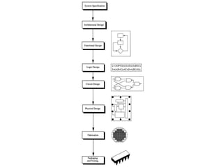
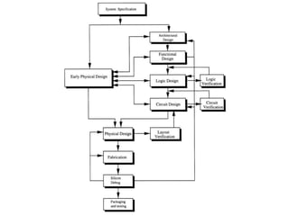
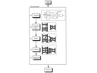
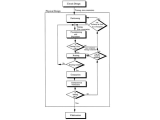
VLSI Design Automation
• This rapid growth in integration technology
has been made possible by the automation of
various steps involved in the design and
fabrication of VLSI chips.
• Integrated circuits consist of a number of
electronic components, built by layering
several different materials in a well-defined
fashion on a silicon base called a wafer.
VLSI Design Automation
• The designer of an IC transforms a circuit
description into a geometric description,
called the layout.
• A layout consists of a set of planar geometric
shapes in several layers.
• The layout is checked to ensure that it meets
all the design requirements.
• The result is a set of design files that describes
the layout.
VLSI Design Automation
• An optical pattern generator is used to convert
the design files into pattern generator files.
• These files are used to produce patterns called
masks.
• During fabrication, these masks are used to
pattern a silicon wafer using a sequence of photo-
lithographic steps.
• The component formation requires very exacting
details about geometric patterns and the
separation between them.
VLSI Design Automation
• The process of converting the specification of an
electrical circuit into a layout is called the physical
design process.
• Due to the tight tolerance requirements and the
extremely small size of the individual
components, physical design is an extremely
tedious and error prone process.
• Due to the large number of components, and the
exacting details required by the fabrication
process, physical design is not practical without
the help of computers.
VLSI Design Automation
• As a result, almost all phases of physical design
extensively use Computer Aided Design (CAD) tools,
and many phases have already been partially or fully
automated.
• VLSI Physical Design Automation is essentially the
research, development and productization of
algorithms and data structures related to the physical
design process.
• The objective is to investigate optimal arrangements of
devices on a plane and efficient interconnection
schemes between these devices to obtain the desired
functionality and performance.
VLSI Design Automation
• Since space on a wafer is very expensive real
estate, algorithms must use the space very
efficiently to lower costs and improve yield.
• In addition, the arrangement of devices plays
a key role in determining the performance of a
chip.
• Algorithms for physical design must also
ensure that the layout generated abides by all
the rules required by the fabrication process.
VLSI Design Automation
• Fabrication rules establish the tolerance limits of
the fabrication process.
• Finally, algorithms must be efficient and should
be able to handle very large designs.
• Efficient algorithms not only lead to fast turn-
around time, but also permit designers to make
iterative improvements to the layouts.
• The VLSI physical design process manipulates
very simple geometric objects, such as polygons
and lines.
VLSI Design Automation
• As a result, physical design algorithms tend to be very
intuitive in nature, and have significant overlap with
graph algorithms and combinatorial optimization
algorithms.
• In view of this observation, many consider physical
design automation the study of graph theoretic and
combinatorial algorithms for manipulation of
geometric objects in two and three dimensions.
• However, a pure geometric point of view ignores the
electrical (both digital and analog) aspect of the
physical design problem.
VLSI Design Automation
• In a VLSI circuit, polygons and lines have inter-
related electrical properties, which exhibit a
very complex behavior and depend on a host
of variables.
• Therefore, it is necessary to keep the electrical
aspects of the geometric objects in
perspective while developing algorithms for
VLSI physical design automation.
VLSI Design Automation
• With the introduction of Very Deep Sub-
Micron (VDSM), which provides very small
features and allows dramatic increases in the
clock frequency, the effect of electrical
parameters on physical design will play a more
dominant role in the design and development
of new algorithms.
VLSI Design Cycle
• The VLSI design cycle starts with a formal
specification of a VLSI chip, follows a series of
steps, and eventually produces a packaged
chip.
• Emphasis is given on the physical design step
of the VLSI design cycle.
VLSI Design Cycle
• System Specification:
– The first step of any design process is to lay down
the specifications of the system. System
specification is a high level representation of the
system. The factors to be considered in this
process include: performance, functionality, and
physical dimensions (size of the die (chip)).
VLSI Design Cycle
• System Specification:
– The fabrication technology and design techniques
are also considered. The specification of a system
is a compromise between market requirements,
technology and economical viability. The end
results are specifications for the size, speed,
power, and functionality of the VLSI system.
VLSI Design Cycle
• Architectural Design
– The basic architecture of the system is designed in
this step. This includes, such decisions as RISC
(Reduced Instruction Set Computer) versus CISC
(Complex Instruction Set Computer), number of
ALUs, Floating Point units, number and structure
of pipelines, and size of caches among others.
VLSI Design Cycle
• Behavioral or Functional Design
– In this step, main functional units of the system
are identified. This also identifies the interconnect
requirements between the units. The area, power,
and other parameters of each unit are estimated.
The behavioral aspects of the system are
considered without implementation specific
information.
VLSI Design Cycle
• Logic Design:
– In this step the control flow, word widths, register
allocation, arithmetic operations, and logic
operations of the design that represent the
functional design are derived and tested. This
description is called Register Transfer Level (RTL)
description. RTL is expressed in a Hardware
Description Language (HDL), such as VHDL or
Verilog.
VLSI Design Cycle
• Circuit Design:
– The purpose of circuit design is to develop a
circuit representation based on the logic design.
The Boolean expressions are converted into a
circuit representation by taking into consideration
the speed and power requirements of the original
design. Circuit Simulation is used to verify the
correctness and timing of each component.
VLSI Design Cycle
• Circuit Design:
– The circuit design is usually expressed in a detailed
circuit diagram. This diagram shows the circuit
elements (cells, macros, gates, transistors) and
interconnection between these elements. This
representation is also called a netlist.
– Tools used to manually enter such description are
called schematic capture tools. In many cases, a
netlist can be created automatically from logic
(RTL) description by using logic synthesis tools.
VLSI Design Cycle
• Physical Design:
– In this step the circuit representation (or netlist) is
converted into a geometric representation. As
stated earlier, this geometric representation of a
circuit is called a layout.
– Layout is created by converting each logic
component (cells, macros, gates, transistors) into
a geometric representation (specific shapes in
multiple layers), which perform the intended logic
function of the corresponding component.
VLSI Design Cycle
• Physical Design:
– Connections between different components are
also expressed as geometric patterns typically
lines in multiple layers.
– The exact details of the layout also depend on
design rules, which are guidelines based on the
limitations of the fabrication process and the
electrical properties of the fabrication materials.
VLSI Design Cycle
• Physical Design:
– Physical design is a very complex process and
therefore it is usually broken down into various
sub-steps.
– Various verification and validation checks are
performed on the layout during physical design.
– In many cases, physical design can be completely
or partially automated and layout can be
generated directly from netlist by Layout Synthesis
tools.
VLSI Design Cycle
• Physical Design:
– Most of the layout of a high performance design
(such as a microprocessor) may be done using
manual design, while many low to medium
performance design or designs which need faster
time-to-market may be done automatically.
– Layout synthesis tools, while fast, do have an area
and performance penalty, which limit their use to
some designs. Manual layout, while slow and
manually intensive, does have better area and
performance as compared to synthesized layout.
VLSI Design Cycle
• Fabrication
– After layout and verification, the design is ready
for fabrication. Since layout data is typically sent
to fabrication on a tape, the event of release of
data is called Tape Out.
– Layout data is converted (or fractured) into photo-
lithographic masks, one for each layer. Masks
identify spaces on the wafer, where certain
materials need to be deposited, diffused or even
removed.
VLSI Design Cycle
• Fabrication:
– Silicon crystals are grown and sliced to produce
wafers. Extremely small dimensions of VLSI
devices require that the wafers be polished to
near perfection.
– The fabrication process consists of several steps
involving deposition, and diffusion of various
materials on the wafer. During each step one mask
is used. Several dozen masks may be used to
complete the fabrication process.
VLSI Design Cycle
• Fabrication
– A large wafer is 20 cm (8 inch) in diameter and can
be used to produce hundreds of chips, depending
of the size of the chip.
– Before the chip is mass produced, a prototype is
made and tested. Industry is rapidly moving
towards a 30 cm (12 inch) wafer allowing even
more chips per wafer leading to lower cost per
chip.
VLSI Design Cycle
• Packaging, Testing and Debugging:
– Finally, the wafer is fabricated and diced into
individual chips in a fabrication facility. Each chip is
then packaged and tested to ensure that it meets all
the design specifications and that it functions
properly.
– Chips used in Printed Circuit Boards (PCBs) are
packaged in Dual In-line Package (DIP), Pin Grid Array
(PGA), Ball Grid Array (BGA), and Quad Flat Package
(QFP).
– Chips used in Multi-Chip Modules (MCM) are not
packaged, since MCMs use bare or naked chips.
VLSI Design Cycle
• It is important to note that design of a
complex VLSI chip is a complex human power
management project as well.
• Several hundred engineers may work on a
large design project for two to three years.
• This includes architecture designers, circuit
designers, physical design specialists, and
design automation engineers.
VLSI Design Cycle
• As a result, design is usually partitioned along
functionality, and different units are designed by
different teams.
• At any given time, each unit may not be at the
same level of design. While one unit may be in
logic design phase, another unit may be
completing its physical design phase.
• This imposes a serious problem for chip level
design tools, since these tools must work with
partial data at the chip level.
VLSI Design Cycle
• The VLSI design cycle involves iterations, both
within a step and between different steps.
• The entire design cycle may be viewed as
transformations of representations in various
steps.
• In each step, a new representation of the
system is created and analyzed. The
representation is iteratively improved to meet
system specifications.
VLSI Design Cycle
• For example, a layout is iteratively improved, so
that it meets the timing specifications of the
system.
• Another example may be detection of design rule
violations during design verification. If such
violations are detected, the physical design step
needs to be repeated to correct the error.
• The objectives of VLSI CAD tools are to minimize
the time for each iteration and the total number
of iterations, thus reducing time-to-market.
New Trends in VLSI Design Cycle
• Increasing interconnect delay
• Increasing interconnect area
• Increasing number of metal layers
• Increasing planning requirements
• Synthesis
– Logic Synthesis
– High Level Synthesis
Increasing interconnect delay
• As the fabrication process improves, the
interconnect is not scaling at the same rate as
the devices.
• Devices are becoming smaller and faster, and
interconnect has not kept up with that pace.
• 60% of a path delay may be due to
interconnect.
• Repeaters are now necessary for most chip
level nets.
Increasing interconnect area
• A microprocessor die has only 60%-70% of its
area covered with active devices.
• The rest of the area is needed to
accommodate the interconnect.
• This area also leads to performance
degradation.
• In early ICs, a few hundred transistors were
interconnected using one layer of metal.
Increasing Interconnect Area
• As the number of transistors grew, the
interconnect area increased.
• However, with the introduction of a second metal
layer, the interconnect area decreased.
• This has been the trend between design
complexity and the number of metal layers.
• In current designs, with approximately ten million
transistors and four to six layers of metal, one
finds about 40% of the chips real estate dedicated
to its interconnect.
Increasing number of metal layers
• To meet the increasing needs of interconnect,
the number of metal layers available for
interconnect is increasing.
• Currently, a three layer process is commonly
used for most designs, while four layer and
five layer processes are used mainly for
microprocessors.
• 3D view of the interconnect is necessary.
Increasing planning requirements
• The most important implication of increasing
interconnect delay, area of the die dedicated
to interconnect, and a large number of metal
layers is that the relative location of devices is
very important.
• Physical design considerations have to enter
into design at a much earlier phase.
• In fact, functional design should include chip
planning.
Increasing planning requirements
• Two new key steps: Block planning and Signal
planning.
• Block planning assigns shapes and locations to
main functional blocks.
• Signal planning refers to assignment of the 3D
regions through which major busses and
signals routed.
• Timing should be estimated to verify the
validity of the chip plan.
Synthesis
• The time required to design any block can be
reduced if layout can be directly generated or
synthesized from a higher level description.
• This not only reduces design time, it also
eliminates human errors.
• The biggest disadvantage is the area used by
synthesized blocks.
• Such blocks take larger areas than hand
crafted blocks.
Logic Synthesis
• This process converts an HDL description of a
block into schematics (circuit description) and
then produces its layout.
• Logic synthesis is an established technology
for blocks in a chip design, and for complete
Application Specific Integrated Circuits (ASICs).
Logic Synthesis
• Logic synthesis is not applicable for large
regular blocks, such as RAMs, ROMs, PLAs and
Datapaths, and complete microprocessor
chips for two reasons: speed and area.
• Logic synthesis tools are too slow and too
area, inefficient to deal with such blocks.
High Level Synthesis
• This process converts a functional or micro-
architectural description into a layout or RTL
description.
• In high level synthesis, input is a description
which captures only the behavioral aspects of the
system.
• Digital Signal Processing (DSP) architectures have
been successfully synthesized by Silicon
Compilers.
• Module Generators, which work on smaller size
problems.
High Level Synthesis
• The basic idea is to simplify the synthesis task,
either by restricting the architecture or restricting
the size of the problem.
• High level synthesis is an area of current research
and is not used in actual chip development.
• High level synthesis systems provide very good
implementations for specialized classes of
systems, and they will continue to gain
acceptance as they become more generalized.
New Trends in VLSI Design Cycle
• Due to increasing interconnect delay, the physical
design starts very early in the design cycle to get
improved estimates of the performance of the chip.
• The early floor physical design activities lead to
increasingly improved chip layout as each block is
refined.
• This also allows better utilization of the chip area to
distribute the interconnect in three dimensions.
• This distribution helps in reducing the die size,
improving yield and reducing cost.
Physical Design Cycle
• The input to the physical design cycle is the
circuit and the output is the layout of the
circuit.
• This is accomplished in several stages such as
partitioning, floorplanning, placement,
routing, and compaction.
Partitioning
• A chip may contain several million transistors.
• Due to the limitations of memory space and
computation power available it may not be
possible to layout the entire chip (or large
circuit) in the same step.
• Therefore, the chip (circuit) is normally
partitioned into sub-chips (sub-circuits). These
sub-partitions are called blocks.
Partitioning
• The actual partitioning process considers many
factors such as the size of the blocks, number of
blocks, and number of interconnections between
the blocks.
• The output of partitioning is a set of blocks and
the interconnections required between blocks.
• In large circuits, the partitioning process is
hierarchical and at the topmost level a chip may
have 5 to 25 blocks.
• Each block is then partitioned recursively into
smaller blocks.
Floorplanning
• This step is concerned with selecting good
layout alternatives for each block, as well as
the entire chip.
• The area of each block can be estimated after
partitioning and is based approximately on the
number and the type of components in that
block.
• In addition, interconnect area required within
the block must be considered.
Floorplanning
• Floorplanning is a critical step, as it sets up the
ground work for a good layout.
• However, it is computationally quite hard.
Very often the task of floorplanning is done by
a design engineer, rather than a CAD tool.
• This is due to the fact that a human is better
at ‘visualizing’ the entire floorplan and taking
into account the information flow.
Floorplanning
• Manual floorplanning is sometimes necessary
as the major components of an IC need to be
placed in accordance with the signal flow of
the chip.
• In addition, certain components are often
required to be located at specific positions on
the chip.
Placement
• During placement, the blocks are exactly
positioned on the chip.
• The goal of placement is to find a minimum area
arrangement for the blocks that allows
completion of interconnections between the
blocks, while meeting the performance
constraints.
• That is, we want to avoid a placement which is
routable but does not allow certain nets to meet
their timing goals.
Placement
• Placement is typically done in two phases.
• In the first phase an initial placement is
created.
• In the second phase, the initial placement is
evaluated and iterative improvements are
made until the layout has minimum area or
best performance and conforms to design
specifications.
Placement
• Some space between the blocks is intentionally
left empty to allow interconnections between
blocks.
• The quality of the placement will not be evident
until the routing phase has been completed.
• Placement may lead to an unroutable design, i.e.,
routing may not be possible in the space
provided.
• In that case, another iteration of placement is
necessary.
Placement
• To limit the number of iterations of the placement
algorithm, an estimate of the required routing space
is used during the placement phase.
• Good routing and circuit performance depend
heavily on a good placement algorithm.
• This is due to the fact that once the position of each
block is fixed, very little can be done to improve the
routing and the overall circuit performance.
• Late placement changes lead to increased die size
and lower quality designs.
Routing
• The objective of the routing phase is to
complete the interconnections between
blocks according to the specified netlist.
• First, the space not occupied by the blocks
(called the routing space) is partitioned into
rectangular regions called channels and
switchboxes.
• This includes the space between the blocks as
well the as the space on top of the blocks.
Routing
• The goal of a router is to complete all circuit
connections using the shortest possible wire
length and using only the channel and switch
boxes.
• This is usually done in two phases, referred to as
the Global Routing and Detailed Routing phases.
• In global routing, connections are completed
between the proper blocks of the circuit
disregarding the exact geometric details of each
wire and pin.
Routing
• For each wire, the global router finds a list of channels
and switchboxes which are to be used as a passageway
for that wire.
• In other words, global routing specifies the different
regions in the routing space through which a wire
should be routed.
• Global routing is followed by detailed routing which
completes point-to-point connections between pins on
the blocks.
• Global routing is converted into exact routing by
specifying geometric information such as the location
and spacing of wires and their layer assignments.
Routing
• Detailed routing includes channel routing and
switchbox routing, and is done for each
channel and switchbox.
• Routing is a very well studied problem, and
several hundred articles have been published
about all its aspects.
• Since almost all problems in routing are
computationally hard, the researchers have
focused on heuristic algorithms.
Routing
• Experimental evaluation has become an integral
part of all algorithms and several benchmarks
have been standardized.
• Due to the very nature of the routing algorithms,
complete routing of all the connections cannot be
guaranteed in many cases.
• As a result, a technique called rip-up and re-route
is used, which basically removes troublesome
connections and reroutes them in a different
order.
Compaction
• Compaction is simply the task of compressing
the layout in all directions such that the total
area is reduced.
• By making the chip smaller, wire lengths are
reduced, which in turn reduces the signal
delay between components of the circuit.
• At the same time, a smaller area may imply
more chips can be produced on a wafer, which
in turn reduces the cost of manufacturing.
Compaction
• However, the expense of computing time
mandates that extensive compaction is used
only for large volume applications, such as
microprocessors.
• Compaction must ensure that no rules
regarding the design and fabrication process
are violated during the process.
Extraction and Verification
• Design Rule Checking (DRC) is a process which
verifies that all geometric patterns meet the
design rules imposed by the fabrication process.
• For example, one typical design rule is the wire
separation rule i.e., the fabrication process
requires a specific separation (in microns)
between two adjacent wires.
• DRC must check such separation for millions of
wires on the chip.
Extraction and Verification
• There may be several dozen design rules,
some of them are quite complicated to check.
• After checking the layout for design rule
violations and removing the design rule
violations, the functionality of the layout is
verified by Circuit Extraction.
• This is a reverse engineering process, and
generates the circuit representation from the
layout.
Extraction and Verification
• The extracted description is compared with the
circuit description to verify its correctness.
• This process is called Layout Versus Schematics (LVS)
verification.
• Geometric information is extracted to compute
Resistance and Capacitance.
• This allows accurate calculation of the timing of each
component, including interconnect.
• This process is called Performance Verification.
Extraction and Verification
• The extracted information is also used to
check the reliability aspects of the layout.
• This process is called Reliability Verification
and it ensures that layout will not fail due to
electromigration, self-heat and other effects.
Summary of Physical Design Cycle
• Physical design, like VLSI design, is iterative in
nature and many steps, such as global routing
and channel routing, are repeated several times
to obtain a better layout.
• In addition, the quality of results obtained in a
step depends on the quality of the solution
obtained in earlier steps.
• For example, a poor quality placement cannot be
‘cured’ by high quality routing. As a result, earlier
steps have more influence on the overall quality
of the solution.
Physical Design Cycle
• In this sense, partitioning, floorplanning, and
placement problems play a more important
role in determining the area and chip
performance, as compared to routing and
compaction.
• Since placement may produce an ‘unroutable’
layout, the chip might need to be re-placed or
re-partitioned before another routing is
attempted.
Physical Design Cycle
• In general, the whole design cycle may be
repeated several times to accomplish the
design objectives.
• The complexity of each step varies, depending
on the design constraints as well as the design
style used.
New Trends in Physical Design Cycle
• As fabrication technology improves and process
enters the deep sub-micron (DSM) range, it is
clear that interconnect delay is not being scaled
at the same rate as the gate delay.
• Therefore, interconnect delay is a more
significant part of overall delay.
• As a result, in high performance chips,
interconnect delay must be considered from very
early design stages.
• In order to reduce interconnect delay several
methods can be employed.
Chip level signal planning
• At the chip level, routing of major signals and
buses must be planned from early design
stages, so that interconnect distances can be
minimized.
• In addition, these global signals must be
routed in the top metal layers, which have low
delay per unit length.
OTC Routing
• Over-the-Cell (OTC) routing is a term used to
describe routing over blocks and active areas.
• It is different from conventional channel and
switchbox routing approach.
• The chip level signal planning is OTC routing
on the entire chip.
• The OTC approach can also be used within a
block to reduce area and improve
performance.
OTC Routing
• The OTC routing approach essentially makes
routing a three dimensional problem.
• Another effect of the OTC routing approach is
that the pins are not brought to the block
boundaries for connections to other blocks.
• Instead, pins are brought to the top of the
block as a sea-of-pins.
• It is called Arbitrary Terminal Model (ATM).
Design Styles
• Physical design is an extremely complex process.
Even after breaking the entire process into
several conceptually easier steps, it has been
shown that each step is computationally very
hard.
• However, market requirements demand quick
time-to-market and high yield. As a result,
restricted models and design styles are used in
order to reduce the complexity of physical design.
Design Styles
• The design styles can be broadly classified as either
full-custom or semi-custom.
• In a full-custom layout, different blocks of a circuit
can be placed at any location on a silicon wafer as
long as all the blocks are non-overlapping.
• On the other hand, in semi-custom layout, some
parts of a circuit are predesigned and placed on
some specific place on the silicon wafer.
• Selection of a layout style depends on many factors
including the type of chip, cost, and time-to-market.
Design Styles
• Full-custom layout is a preferred style for mass
produced chips, since the time required to
produce a highly optimized layout can be
justified.
• On the other hand, to design an Application
Specific Integrated Circuit (ASIC), a semi-
custom layout style is usually preferred.
• On a large chip, each block may use a different
layout design style.
Full-custom Structure
Standard Cell
• The design process in the standard cell design
style is some what simpler than full-custom
design style.
• Standard cell architecture considers the layout
to consist of rectangular cells of the same
height.
• Initially, a circuit is partitioned into several
smaller blocks, each of which is equivalent to
some predefined sub-circuit (cell).
Standard Cell
• The functionality and the electrical characteristics
of each predefined cell are tested, analyzed, and
specified.
• A collection of these cells is called a cell library.
• Usually a cell library consists of 500-1200 cells.
• Terminals on cells may be located either on the
boundary or distributed throughout the cell area.
• Cells are placed in rows and the space between
two rows is called a channel.
Standard Cell
• These channels and the space above and between cells
is used to perform interconnections between cells.
• If two cells to be interconnected lie in the same row or
in adjacent rows, then the channel between the rows is
used for interconnection.
• However, if two cells to be connected lie in two non-
adjacent rows, then their interconnection wire passes
through empty space between any two cells or passes
on top of the cells.
• This empty space between cells in a row is called a
feedthrough.
Gate Arrays
• All the cells in gate array are identical.
• Each chip is an array of identical gates or cells.
• These cells are separated by both vertical and
horizontal spaces called vertical and horizontal
channels.
• The circuit design is modified such that it can be
partitioned into a number of identical blocks.
• Each block must be logically equivalent to a cell
on the gate array.
Gate Arrays
• The name ‘gate array’ signifies the fact that each cell
may simply be a gate, such as a three input NAND
gate.
• The number of partitioned blocks must be less than
or equal to the total number of cells on the chip.
• Once the circuit is partitioned into identical blocks,
the task is to make the interconnections between the
prefabricated cells on the chip using horizontal and
vertical channels to form the actual circuit.
• The gate array wafer is taken into a fabrication facility
and routing layers are fabricated on top of the wafer.
Gate Arrays
Gate Arrays
Field Programmable Gate Arrays
• The Field Programmable Gate Array (FPGA) is a
new approach to ASIC design that can
dramatically reduce manufacturing turn-around
time and cost for low volume manufacturing.
• In FPGAs, cells and interconnect are
prefabricated.
• The user simply ‘programs’ the interconnect.
• FPGA designs provide large scale integration and
user programmability.
Field Programmable Gate Arrays
• A FPGA consists of horizontal rows of
programmable logic blocks which can be
interconnected by a programmable routing
network.
• FPGA cells are more complex than standard cells.
However, almost all the cells have the same
layout.
• A logic block is simply a memory block which can
be programmed to remember the logic table of a
function.
Field Programmable Gate Arrays
• Connection between horizontal segments is
provided through antifuses, whereas the
connection between a horizontal segment and
a vertical segment is provided through a cross
fuse.
FPGA
FPGA
FPGA
• The cross fuses are shown as circles, while
antifuses are shown as rectangles.
• One disadvantage of fuse based FPGAs is that
they are not reprogrammable.
• There are other types of FPGAs which allow
re-programming, and use pass gates rather
than programmable fuses.
Data Structures and Basic
Algorithms
• Physical design CAD tools require highly
specialized algorithms and data structures to
effectively manage and manipulate layout
information.
• These tools fall in three categories.
• The first type of tools help a human designer
to manipulate a layout.
– For example, a layout editor allows designers to
add transistors or nets to a layout.
Data Structures and Basic
Algorithms
• The second type of tools are designed to
perform some task on the layout
automatically.
– Example of such tools include channel routers and
placement tools.
– It is also possible to invoke a tool of second type
from the layout editor.
Data Structures and Basic
Algorithms
• The third type of tools are used for checking
and verification.
– Example of such tools include; DRC (design rule
checker) and LVS verifier (layout versus schematics
verifier).
• Most of the research of physical design
automation has focused on tools of the last
two types whereas most attention is given to
the 2nd type.
Data Structures and Basic
Algorithms
• The major focus has been on development on
design and analysis of heuristic algorithms for
partitioning, placement, routing and
compaction.
• Many of these algorithms are based on graph
theory and computational geometry.
Basic Terminology
• A graph is a pair of sets G = (V, E), where V is a
set of vertices, and E is a set of pairs of distinct
vertices called edges.
• V(G) and E(G) refer to the vertex and edge set
of a graph G.
• A vertex u is adjacent to a vertex v, if is an
edge i.e.
• The set of vertices adjacent to is
  E
v
u 
,
 
v
u,
v  
v
Adj
Basic Terminology
• An edge is incident on the vertices
and which are the ends of e.
• The degree of a vertex is the number of
edges incident with the vertex .
• A complete graph on vertices is a graph in
which each vertex is adjacent to every other
vertex.
• is used to denote the graph.
 
v
u
e ,
 u
v
v
u
n
n
K
Basic Terminology
• A graph H is called the complement of graph G
= (V, E), if H = (V, F), where, .
  E
K
E
F v


Complexity Issues and NP-hardness
• Several general algorithms and mathematical
techniques are frequently used to develop
algorithms for physical design.
– Greedy Algorithms
– Divide and Conquer Algorithms
– Dynamic Programming Algorithms
– Network Flow Algorithms
– Linear/Integer Programming Techniques
Complexity Issues and NP-hardness
• The class of solvable problems can be
partitioned into two general classes, P and NP.
• The class P consists of all problems that can be
solved by a deterministic turing machine in
polynomial time.
• A conventional computer may be viewed as
such a machine. Minimum cost spanning tree,
single source shortest path, and graph
matching problems belong to class P.
Complexity Issues and NP-hardness
• The other class called NP, consists of problems
that can be solved in polynomial time by a
nondeterministic turing machine.
• This type of turing machine may be viewed as
a parallel computer with as many processors
as we may need.
• If every problem in class NP can be reduced to
a problem P, then problem P is in class NP-
complete.
Complexity Issues and NP-hardness
• Several thousand problems in computer
science, graph theory, combinatorics,
operations research, and computational
geometry have been proven to be NP
complete.
• The optimization version of a problem P, is
called NP-hard, if the decision version of the
problem P is NP-complete.
Algorithms for NP-hard Problems
• Most optimization problems in physical design
are NP-hard.
• If a problem is known to be NP-complete or
NP-hard, then it is unlikely that a polynomial
time algorithm exists for that problem.
Exponential Algorithms
• If the size of the input is small, then algorithms
with exponential time complexity may be
feasible.
• In many cases, the solution of a certain problem
be critical to the performance of the chip and
therefore it is practical to spend extra resources
to solve that problem optimally.
• One such exponential method is integer
programming, which has been very successfully
used to solve many physical design problems.
Graph Search Algorithms
• Since many problems in physical design are
modeled using graphs.
• It is important to understand efficient
methods for searching graphs.
– Depth-First Search
– Breadth-First Search
– Topological Search
Depth-First Search
• In this graph search strategy, graph is searched
‘as deeply as possible’.
• In Depth-First Search (DFS), an edge is
selected for further exploration from the most
recently visited vertex.
• When all the edges of have been explored, the
algorithm back tracks to the previous vertex,
which may have an unexplored edge.
Depth-First Search
• The algorithm uses an array MARKED (n)
which is initialized to zero before calling the
algorithm to keep track of all the visited
vertices.
• It is easy to see that the time complexity of
depth-first search is O(|V| +|E|).
Graph Search Algorithms
• Depth-First Search:
Breadth-First Search
• The basic idea of Breadth-First Search (BFS) is to
explore all vertices adjacent to a vertex before
exploring any other vertex.
• Starting with a source vertex , the BFS first
explores all edges of , puts the reachable vertices
in a queue, and marks the vertex as visited.
• If a vertex is already marked visited then it is not
enqueued. This process is repeated for each
vertex in the queue.
Breadth-First Search
• This process of visiting edges produces a BFS
tree.
• The BFS algorithm can be used to search both
directed and undirected graphs.
• the main difference between the DFS and the
BFS is that the DFS uses a stack (recursion is
implemented using stacks), while the BFS uses
a queue as its data structure.
Breadth-First Search
• The time complexity of breadth first search is
also O(|V| + |E|).
Algorithms for NP-hard Problems

VLSI Physical Design Automation.ppt

  • 1.
    VLSI Design Automation •This rapid growth in integration technology has been made possible by the automation of various steps involved in the design and fabrication of VLSI chips. • Integrated circuits consist of a number of electronic components, built by layering several different materials in a well-defined fashion on a silicon base called a wafer.
  • 2.
    VLSI Design Automation •The designer of an IC transforms a circuit description into a geometric description, called the layout. • A layout consists of a set of planar geometric shapes in several layers. • The layout is checked to ensure that it meets all the design requirements. • The result is a set of design files that describes the layout.
  • 3.
    VLSI Design Automation •An optical pattern generator is used to convert the design files into pattern generator files. • These files are used to produce patterns called masks. • During fabrication, these masks are used to pattern a silicon wafer using a sequence of photo- lithographic steps. • The component formation requires very exacting details about geometric patterns and the separation between them.
  • 4.
    VLSI Design Automation •The process of converting the specification of an electrical circuit into a layout is called the physical design process. • Due to the tight tolerance requirements and the extremely small size of the individual components, physical design is an extremely tedious and error prone process. • Due to the large number of components, and the exacting details required by the fabrication process, physical design is not practical without the help of computers.
  • 5.
    VLSI Design Automation •As a result, almost all phases of physical design extensively use Computer Aided Design (CAD) tools, and many phases have already been partially or fully automated. • VLSI Physical Design Automation is essentially the research, development and productization of algorithms and data structures related to the physical design process. • The objective is to investigate optimal arrangements of devices on a plane and efficient interconnection schemes between these devices to obtain the desired functionality and performance.
  • 6.
    VLSI Design Automation •Since space on a wafer is very expensive real estate, algorithms must use the space very efficiently to lower costs and improve yield. • In addition, the arrangement of devices plays a key role in determining the performance of a chip. • Algorithms for physical design must also ensure that the layout generated abides by all the rules required by the fabrication process.
  • 7.
    VLSI Design Automation •Fabrication rules establish the tolerance limits of the fabrication process. • Finally, algorithms must be efficient and should be able to handle very large designs. • Efficient algorithms not only lead to fast turn- around time, but also permit designers to make iterative improvements to the layouts. • The VLSI physical design process manipulates very simple geometric objects, such as polygons and lines.
  • 8.
    VLSI Design Automation •As a result, physical design algorithms tend to be very intuitive in nature, and have significant overlap with graph algorithms and combinatorial optimization algorithms. • In view of this observation, many consider physical design automation the study of graph theoretic and combinatorial algorithms for manipulation of geometric objects in two and three dimensions. • However, a pure geometric point of view ignores the electrical (both digital and analog) aspect of the physical design problem.
  • 9.
    VLSI Design Automation •In a VLSI circuit, polygons and lines have inter- related electrical properties, which exhibit a very complex behavior and depend on a host of variables. • Therefore, it is necessary to keep the electrical aspects of the geometric objects in perspective while developing algorithms for VLSI physical design automation.
  • 10.
    VLSI Design Automation •With the introduction of Very Deep Sub- Micron (VDSM), which provides very small features and allows dramatic increases in the clock frequency, the effect of electrical parameters on physical design will play a more dominant role in the design and development of new algorithms.
  • 11.
    VLSI Design Cycle •The VLSI design cycle starts with a formal specification of a VLSI chip, follows a series of steps, and eventually produces a packaged chip. • Emphasis is given on the physical design step of the VLSI design cycle.
  • 13.
    VLSI Design Cycle •System Specification: – The first step of any design process is to lay down the specifications of the system. System specification is a high level representation of the system. The factors to be considered in this process include: performance, functionality, and physical dimensions (size of the die (chip)).
  • 14.
    VLSI Design Cycle •System Specification: – The fabrication technology and design techniques are also considered. The specification of a system is a compromise between market requirements, technology and economical viability. The end results are specifications for the size, speed, power, and functionality of the VLSI system.
  • 15.
    VLSI Design Cycle •Architectural Design – The basic architecture of the system is designed in this step. This includes, such decisions as RISC (Reduced Instruction Set Computer) versus CISC (Complex Instruction Set Computer), number of ALUs, Floating Point units, number and structure of pipelines, and size of caches among others.
  • 16.
    VLSI Design Cycle •Behavioral or Functional Design – In this step, main functional units of the system are identified. This also identifies the interconnect requirements between the units. The area, power, and other parameters of each unit are estimated. The behavioral aspects of the system are considered without implementation specific information.
  • 17.
    VLSI Design Cycle •Logic Design: – In this step the control flow, word widths, register allocation, arithmetic operations, and logic operations of the design that represent the functional design are derived and tested. This description is called Register Transfer Level (RTL) description. RTL is expressed in a Hardware Description Language (HDL), such as VHDL or Verilog.
  • 18.
    VLSI Design Cycle •Circuit Design: – The purpose of circuit design is to develop a circuit representation based on the logic design. The Boolean expressions are converted into a circuit representation by taking into consideration the speed and power requirements of the original design. Circuit Simulation is used to verify the correctness and timing of each component.
  • 19.
    VLSI Design Cycle •Circuit Design: – The circuit design is usually expressed in a detailed circuit diagram. This diagram shows the circuit elements (cells, macros, gates, transistors) and interconnection between these elements. This representation is also called a netlist. – Tools used to manually enter such description are called schematic capture tools. In many cases, a netlist can be created automatically from logic (RTL) description by using logic synthesis tools.
  • 20.
    VLSI Design Cycle •Physical Design: – In this step the circuit representation (or netlist) is converted into a geometric representation. As stated earlier, this geometric representation of a circuit is called a layout. – Layout is created by converting each logic component (cells, macros, gates, transistors) into a geometric representation (specific shapes in multiple layers), which perform the intended logic function of the corresponding component.
  • 21.
    VLSI Design Cycle •Physical Design: – Connections between different components are also expressed as geometric patterns typically lines in multiple layers. – The exact details of the layout also depend on design rules, which are guidelines based on the limitations of the fabrication process and the electrical properties of the fabrication materials.
  • 22.
    VLSI Design Cycle •Physical Design: – Physical design is a very complex process and therefore it is usually broken down into various sub-steps. – Various verification and validation checks are performed on the layout during physical design. – In many cases, physical design can be completely or partially automated and layout can be generated directly from netlist by Layout Synthesis tools.
  • 23.
    VLSI Design Cycle •Physical Design: – Most of the layout of a high performance design (such as a microprocessor) may be done using manual design, while many low to medium performance design or designs which need faster time-to-market may be done automatically. – Layout synthesis tools, while fast, do have an area and performance penalty, which limit their use to some designs. Manual layout, while slow and manually intensive, does have better area and performance as compared to synthesized layout.
  • 24.
    VLSI Design Cycle •Fabrication – After layout and verification, the design is ready for fabrication. Since layout data is typically sent to fabrication on a tape, the event of release of data is called Tape Out. – Layout data is converted (or fractured) into photo- lithographic masks, one for each layer. Masks identify spaces on the wafer, where certain materials need to be deposited, diffused or even removed.
  • 25.
    VLSI Design Cycle •Fabrication: – Silicon crystals are grown and sliced to produce wafers. Extremely small dimensions of VLSI devices require that the wafers be polished to near perfection. – The fabrication process consists of several steps involving deposition, and diffusion of various materials on the wafer. During each step one mask is used. Several dozen masks may be used to complete the fabrication process.
  • 26.
    VLSI Design Cycle •Fabrication – A large wafer is 20 cm (8 inch) in diameter and can be used to produce hundreds of chips, depending of the size of the chip. – Before the chip is mass produced, a prototype is made and tested. Industry is rapidly moving towards a 30 cm (12 inch) wafer allowing even more chips per wafer leading to lower cost per chip.
  • 27.
    VLSI Design Cycle •Packaging, Testing and Debugging: – Finally, the wafer is fabricated and diced into individual chips in a fabrication facility. Each chip is then packaged and tested to ensure that it meets all the design specifications and that it functions properly. – Chips used in Printed Circuit Boards (PCBs) are packaged in Dual In-line Package (DIP), Pin Grid Array (PGA), Ball Grid Array (BGA), and Quad Flat Package (QFP). – Chips used in Multi-Chip Modules (MCM) are not packaged, since MCMs use bare or naked chips.
  • 28.
    VLSI Design Cycle •It is important to note that design of a complex VLSI chip is a complex human power management project as well. • Several hundred engineers may work on a large design project for two to three years. • This includes architecture designers, circuit designers, physical design specialists, and design automation engineers.
  • 29.
    VLSI Design Cycle •As a result, design is usually partitioned along functionality, and different units are designed by different teams. • At any given time, each unit may not be at the same level of design. While one unit may be in logic design phase, another unit may be completing its physical design phase. • This imposes a serious problem for chip level design tools, since these tools must work with partial data at the chip level.
  • 30.
    VLSI Design Cycle •The VLSI design cycle involves iterations, both within a step and between different steps. • The entire design cycle may be viewed as transformations of representations in various steps. • In each step, a new representation of the system is created and analyzed. The representation is iteratively improved to meet system specifications.
  • 31.
    VLSI Design Cycle •For example, a layout is iteratively improved, so that it meets the timing specifications of the system. • Another example may be detection of design rule violations during design verification. If such violations are detected, the physical design step needs to be repeated to correct the error. • The objectives of VLSI CAD tools are to minimize the time for each iteration and the total number of iterations, thus reducing time-to-market.
  • 32.
    New Trends inVLSI Design Cycle • Increasing interconnect delay • Increasing interconnect area • Increasing number of metal layers • Increasing planning requirements • Synthesis – Logic Synthesis – High Level Synthesis
  • 33.
    Increasing interconnect delay •As the fabrication process improves, the interconnect is not scaling at the same rate as the devices. • Devices are becoming smaller and faster, and interconnect has not kept up with that pace. • 60% of a path delay may be due to interconnect. • Repeaters are now necessary for most chip level nets.
  • 34.
    Increasing interconnect area •A microprocessor die has only 60%-70% of its area covered with active devices. • The rest of the area is needed to accommodate the interconnect. • This area also leads to performance degradation. • In early ICs, a few hundred transistors were interconnected using one layer of metal.
  • 35.
    Increasing Interconnect Area •As the number of transistors grew, the interconnect area increased. • However, with the introduction of a second metal layer, the interconnect area decreased. • This has been the trend between design complexity and the number of metal layers. • In current designs, with approximately ten million transistors and four to six layers of metal, one finds about 40% of the chips real estate dedicated to its interconnect.
  • 36.
    Increasing number ofmetal layers • To meet the increasing needs of interconnect, the number of metal layers available for interconnect is increasing. • Currently, a three layer process is commonly used for most designs, while four layer and five layer processes are used mainly for microprocessors. • 3D view of the interconnect is necessary.
  • 37.
    Increasing planning requirements •The most important implication of increasing interconnect delay, area of the die dedicated to interconnect, and a large number of metal layers is that the relative location of devices is very important. • Physical design considerations have to enter into design at a much earlier phase. • In fact, functional design should include chip planning.
  • 38.
    Increasing planning requirements •Two new key steps: Block planning and Signal planning. • Block planning assigns shapes and locations to main functional blocks. • Signal planning refers to assignment of the 3D regions through which major busses and signals routed. • Timing should be estimated to verify the validity of the chip plan.
  • 39.
    Synthesis • The timerequired to design any block can be reduced if layout can be directly generated or synthesized from a higher level description. • This not only reduces design time, it also eliminates human errors. • The biggest disadvantage is the area used by synthesized blocks. • Such blocks take larger areas than hand crafted blocks.
  • 40.
    Logic Synthesis • Thisprocess converts an HDL description of a block into schematics (circuit description) and then produces its layout. • Logic synthesis is an established technology for blocks in a chip design, and for complete Application Specific Integrated Circuits (ASICs).
  • 41.
    Logic Synthesis • Logicsynthesis is not applicable for large regular blocks, such as RAMs, ROMs, PLAs and Datapaths, and complete microprocessor chips for two reasons: speed and area. • Logic synthesis tools are too slow and too area, inefficient to deal with such blocks.
  • 42.
    High Level Synthesis •This process converts a functional or micro- architectural description into a layout or RTL description. • In high level synthesis, input is a description which captures only the behavioral aspects of the system. • Digital Signal Processing (DSP) architectures have been successfully synthesized by Silicon Compilers. • Module Generators, which work on smaller size problems.
  • 43.
    High Level Synthesis •The basic idea is to simplify the synthesis task, either by restricting the architecture or restricting the size of the problem. • High level synthesis is an area of current research and is not used in actual chip development. • High level synthesis systems provide very good implementations for specialized classes of systems, and they will continue to gain acceptance as they become more generalized.
  • 44.
    New Trends inVLSI Design Cycle • Due to increasing interconnect delay, the physical design starts very early in the design cycle to get improved estimates of the performance of the chip. • The early floor physical design activities lead to increasingly improved chip layout as each block is refined. • This also allows better utilization of the chip area to distribute the interconnect in three dimensions. • This distribution helps in reducing the die size, improving yield and reducing cost.
  • 46.
    Physical Design Cycle •The input to the physical design cycle is the circuit and the output is the layout of the circuit. • This is accomplished in several stages such as partitioning, floorplanning, placement, routing, and compaction.
  • 48.
    Partitioning • A chipmay contain several million transistors. • Due to the limitations of memory space and computation power available it may not be possible to layout the entire chip (or large circuit) in the same step. • Therefore, the chip (circuit) is normally partitioned into sub-chips (sub-circuits). These sub-partitions are called blocks.
  • 49.
    Partitioning • The actualpartitioning process considers many factors such as the size of the blocks, number of blocks, and number of interconnections between the blocks. • The output of partitioning is a set of blocks and the interconnections required between blocks. • In large circuits, the partitioning process is hierarchical and at the topmost level a chip may have 5 to 25 blocks. • Each block is then partitioned recursively into smaller blocks.
  • 50.
    Floorplanning • This stepis concerned with selecting good layout alternatives for each block, as well as the entire chip. • The area of each block can be estimated after partitioning and is based approximately on the number and the type of components in that block. • In addition, interconnect area required within the block must be considered.
  • 51.
    Floorplanning • Floorplanning isa critical step, as it sets up the ground work for a good layout. • However, it is computationally quite hard. Very often the task of floorplanning is done by a design engineer, rather than a CAD tool. • This is due to the fact that a human is better at ‘visualizing’ the entire floorplan and taking into account the information flow.
  • 52.
    Floorplanning • Manual floorplanningis sometimes necessary as the major components of an IC need to be placed in accordance with the signal flow of the chip. • In addition, certain components are often required to be located at specific positions on the chip.
  • 53.
    Placement • During placement,the blocks are exactly positioned on the chip. • The goal of placement is to find a minimum area arrangement for the blocks that allows completion of interconnections between the blocks, while meeting the performance constraints. • That is, we want to avoid a placement which is routable but does not allow certain nets to meet their timing goals.
  • 54.
    Placement • Placement istypically done in two phases. • In the first phase an initial placement is created. • In the second phase, the initial placement is evaluated and iterative improvements are made until the layout has minimum area or best performance and conforms to design specifications.
  • 55.
    Placement • Some spacebetween the blocks is intentionally left empty to allow interconnections between blocks. • The quality of the placement will not be evident until the routing phase has been completed. • Placement may lead to an unroutable design, i.e., routing may not be possible in the space provided. • In that case, another iteration of placement is necessary.
  • 56.
    Placement • To limitthe number of iterations of the placement algorithm, an estimate of the required routing space is used during the placement phase. • Good routing and circuit performance depend heavily on a good placement algorithm. • This is due to the fact that once the position of each block is fixed, very little can be done to improve the routing and the overall circuit performance. • Late placement changes lead to increased die size and lower quality designs.
  • 57.
    Routing • The objectiveof the routing phase is to complete the interconnections between blocks according to the specified netlist. • First, the space not occupied by the blocks (called the routing space) is partitioned into rectangular regions called channels and switchboxes. • This includes the space between the blocks as well the as the space on top of the blocks.
  • 58.
    Routing • The goalof a router is to complete all circuit connections using the shortest possible wire length and using only the channel and switch boxes. • This is usually done in two phases, referred to as the Global Routing and Detailed Routing phases. • In global routing, connections are completed between the proper blocks of the circuit disregarding the exact geometric details of each wire and pin.
  • 59.
    Routing • For eachwire, the global router finds a list of channels and switchboxes which are to be used as a passageway for that wire. • In other words, global routing specifies the different regions in the routing space through which a wire should be routed. • Global routing is followed by detailed routing which completes point-to-point connections between pins on the blocks. • Global routing is converted into exact routing by specifying geometric information such as the location and spacing of wires and their layer assignments.
  • 60.
    Routing • Detailed routingincludes channel routing and switchbox routing, and is done for each channel and switchbox. • Routing is a very well studied problem, and several hundred articles have been published about all its aspects. • Since almost all problems in routing are computationally hard, the researchers have focused on heuristic algorithms.
  • 61.
    Routing • Experimental evaluationhas become an integral part of all algorithms and several benchmarks have been standardized. • Due to the very nature of the routing algorithms, complete routing of all the connections cannot be guaranteed in many cases. • As a result, a technique called rip-up and re-route is used, which basically removes troublesome connections and reroutes them in a different order.
  • 62.
    Compaction • Compaction issimply the task of compressing the layout in all directions such that the total area is reduced. • By making the chip smaller, wire lengths are reduced, which in turn reduces the signal delay between components of the circuit. • At the same time, a smaller area may imply more chips can be produced on a wafer, which in turn reduces the cost of manufacturing.
  • 63.
    Compaction • However, theexpense of computing time mandates that extensive compaction is used only for large volume applications, such as microprocessors. • Compaction must ensure that no rules regarding the design and fabrication process are violated during the process.
  • 64.
    Extraction and Verification •Design Rule Checking (DRC) is a process which verifies that all geometric patterns meet the design rules imposed by the fabrication process. • For example, one typical design rule is the wire separation rule i.e., the fabrication process requires a specific separation (in microns) between two adjacent wires. • DRC must check such separation for millions of wires on the chip.
  • 65.
    Extraction and Verification •There may be several dozen design rules, some of them are quite complicated to check. • After checking the layout for design rule violations and removing the design rule violations, the functionality of the layout is verified by Circuit Extraction. • This is a reverse engineering process, and generates the circuit representation from the layout.
  • 66.
    Extraction and Verification •The extracted description is compared with the circuit description to verify its correctness. • This process is called Layout Versus Schematics (LVS) verification. • Geometric information is extracted to compute Resistance and Capacitance. • This allows accurate calculation of the timing of each component, including interconnect. • This process is called Performance Verification.
  • 67.
    Extraction and Verification •The extracted information is also used to check the reliability aspects of the layout. • This process is called Reliability Verification and it ensures that layout will not fail due to electromigration, self-heat and other effects.
  • 69.
    Summary of PhysicalDesign Cycle • Physical design, like VLSI design, is iterative in nature and many steps, such as global routing and channel routing, are repeated several times to obtain a better layout. • In addition, the quality of results obtained in a step depends on the quality of the solution obtained in earlier steps. • For example, a poor quality placement cannot be ‘cured’ by high quality routing. As a result, earlier steps have more influence on the overall quality of the solution.
  • 70.
    Physical Design Cycle •In this sense, partitioning, floorplanning, and placement problems play a more important role in determining the area and chip performance, as compared to routing and compaction. • Since placement may produce an ‘unroutable’ layout, the chip might need to be re-placed or re-partitioned before another routing is attempted.
  • 71.
    Physical Design Cycle •In general, the whole design cycle may be repeated several times to accomplish the design objectives. • The complexity of each step varies, depending on the design constraints as well as the design style used.
  • 72.
    New Trends inPhysical Design Cycle • As fabrication technology improves and process enters the deep sub-micron (DSM) range, it is clear that interconnect delay is not being scaled at the same rate as the gate delay. • Therefore, interconnect delay is a more significant part of overall delay. • As a result, in high performance chips, interconnect delay must be considered from very early design stages. • In order to reduce interconnect delay several methods can be employed.
  • 73.
    Chip level signalplanning • At the chip level, routing of major signals and buses must be planned from early design stages, so that interconnect distances can be minimized. • In addition, these global signals must be routed in the top metal layers, which have low delay per unit length.
  • 74.
    OTC Routing • Over-the-Cell(OTC) routing is a term used to describe routing over blocks and active areas. • It is different from conventional channel and switchbox routing approach. • The chip level signal planning is OTC routing on the entire chip. • The OTC approach can also be used within a block to reduce area and improve performance.
  • 75.
    OTC Routing • TheOTC routing approach essentially makes routing a three dimensional problem. • Another effect of the OTC routing approach is that the pins are not brought to the block boundaries for connections to other blocks. • Instead, pins are brought to the top of the block as a sea-of-pins. • It is called Arbitrary Terminal Model (ATM).
  • 77.
    Design Styles • Physicaldesign is an extremely complex process. Even after breaking the entire process into several conceptually easier steps, it has been shown that each step is computationally very hard. • However, market requirements demand quick time-to-market and high yield. As a result, restricted models and design styles are used in order to reduce the complexity of physical design.
  • 78.
    Design Styles • Thedesign styles can be broadly classified as either full-custom or semi-custom. • In a full-custom layout, different blocks of a circuit can be placed at any location on a silicon wafer as long as all the blocks are non-overlapping. • On the other hand, in semi-custom layout, some parts of a circuit are predesigned and placed on some specific place on the silicon wafer. • Selection of a layout style depends on many factors including the type of chip, cost, and time-to-market.
  • 79.
    Design Styles • Full-customlayout is a preferred style for mass produced chips, since the time required to produce a highly optimized layout can be justified. • On the other hand, to design an Application Specific Integrated Circuit (ASIC), a semi- custom layout style is usually preferred. • On a large chip, each block may use a different layout design style.
  • 80.
  • 81.
    Standard Cell • Thedesign process in the standard cell design style is some what simpler than full-custom design style. • Standard cell architecture considers the layout to consist of rectangular cells of the same height. • Initially, a circuit is partitioned into several smaller blocks, each of which is equivalent to some predefined sub-circuit (cell).
  • 82.
    Standard Cell • Thefunctionality and the electrical characteristics of each predefined cell are tested, analyzed, and specified. • A collection of these cells is called a cell library. • Usually a cell library consists of 500-1200 cells. • Terminals on cells may be located either on the boundary or distributed throughout the cell area. • Cells are placed in rows and the space between two rows is called a channel.
  • 83.
    Standard Cell • Thesechannels and the space above and between cells is used to perform interconnections between cells. • If two cells to be interconnected lie in the same row or in adjacent rows, then the channel between the rows is used for interconnection. • However, if two cells to be connected lie in two non- adjacent rows, then their interconnection wire passes through empty space between any two cells or passes on top of the cells. • This empty space between cells in a row is called a feedthrough.
  • 85.
    Gate Arrays • Allthe cells in gate array are identical. • Each chip is an array of identical gates or cells. • These cells are separated by both vertical and horizontal spaces called vertical and horizontal channels. • The circuit design is modified such that it can be partitioned into a number of identical blocks. • Each block must be logically equivalent to a cell on the gate array.
  • 86.
    Gate Arrays • Thename ‘gate array’ signifies the fact that each cell may simply be a gate, such as a three input NAND gate. • The number of partitioned blocks must be less than or equal to the total number of cells on the chip. • Once the circuit is partitioned into identical blocks, the task is to make the interconnections between the prefabricated cells on the chip using horizontal and vertical channels to form the actual circuit. • The gate array wafer is taken into a fabrication facility and routing layers are fabricated on top of the wafer.
  • 87.
  • 88.
  • 89.
    Field Programmable GateArrays • The Field Programmable Gate Array (FPGA) is a new approach to ASIC design that can dramatically reduce manufacturing turn-around time and cost for low volume manufacturing. • In FPGAs, cells and interconnect are prefabricated. • The user simply ‘programs’ the interconnect. • FPGA designs provide large scale integration and user programmability.
  • 90.
    Field Programmable GateArrays • A FPGA consists of horizontal rows of programmable logic blocks which can be interconnected by a programmable routing network. • FPGA cells are more complex than standard cells. However, almost all the cells have the same layout. • A logic block is simply a memory block which can be programmed to remember the logic table of a function.
  • 91.
    Field Programmable GateArrays • Connection between horizontal segments is provided through antifuses, whereas the connection between a horizontal segment and a vertical segment is provided through a cross fuse.
  • 92.
  • 93.
  • 94.
    FPGA • The crossfuses are shown as circles, while antifuses are shown as rectangles. • One disadvantage of fuse based FPGAs is that they are not reprogrammable. • There are other types of FPGAs which allow re-programming, and use pass gates rather than programmable fuses.
  • 95.
    Data Structures andBasic Algorithms • Physical design CAD tools require highly specialized algorithms and data structures to effectively manage and manipulate layout information. • These tools fall in three categories. • The first type of tools help a human designer to manipulate a layout. – For example, a layout editor allows designers to add transistors or nets to a layout.
  • 96.
    Data Structures andBasic Algorithms • The second type of tools are designed to perform some task on the layout automatically. – Example of such tools include channel routers and placement tools. – It is also possible to invoke a tool of second type from the layout editor.
  • 97.
    Data Structures andBasic Algorithms • The third type of tools are used for checking and verification. – Example of such tools include; DRC (design rule checker) and LVS verifier (layout versus schematics verifier). • Most of the research of physical design automation has focused on tools of the last two types whereas most attention is given to the 2nd type.
  • 98.
    Data Structures andBasic Algorithms • The major focus has been on development on design and analysis of heuristic algorithms for partitioning, placement, routing and compaction. • Many of these algorithms are based on graph theory and computational geometry.
  • 99.
    Basic Terminology • Agraph is a pair of sets G = (V, E), where V is a set of vertices, and E is a set of pairs of distinct vertices called edges. • V(G) and E(G) refer to the vertex and edge set of a graph G. • A vertex u is adjacent to a vertex v, if is an edge i.e. • The set of vertices adjacent to is   E v u  ,   v u, v   v Adj
  • 100.
    Basic Terminology • Anedge is incident on the vertices and which are the ends of e. • The degree of a vertex is the number of edges incident with the vertex . • A complete graph on vertices is a graph in which each vertex is adjacent to every other vertex. • is used to denote the graph.   v u e ,  u v v u n n K
  • 101.
    Basic Terminology • Agraph H is called the complement of graph G = (V, E), if H = (V, F), where, .   E K E F v  
  • 102.
    Complexity Issues andNP-hardness • Several general algorithms and mathematical techniques are frequently used to develop algorithms for physical design. – Greedy Algorithms – Divide and Conquer Algorithms – Dynamic Programming Algorithms – Network Flow Algorithms – Linear/Integer Programming Techniques
  • 103.
    Complexity Issues andNP-hardness • The class of solvable problems can be partitioned into two general classes, P and NP. • The class P consists of all problems that can be solved by a deterministic turing machine in polynomial time. • A conventional computer may be viewed as such a machine. Minimum cost spanning tree, single source shortest path, and graph matching problems belong to class P.
  • 104.
    Complexity Issues andNP-hardness • The other class called NP, consists of problems that can be solved in polynomial time by a nondeterministic turing machine. • This type of turing machine may be viewed as a parallel computer with as many processors as we may need. • If every problem in class NP can be reduced to a problem P, then problem P is in class NP- complete.
  • 105.
    Complexity Issues andNP-hardness • Several thousand problems in computer science, graph theory, combinatorics, operations research, and computational geometry have been proven to be NP complete. • The optimization version of a problem P, is called NP-hard, if the decision version of the problem P is NP-complete.
  • 106.
    Algorithms for NP-hardProblems • Most optimization problems in physical design are NP-hard. • If a problem is known to be NP-complete or NP-hard, then it is unlikely that a polynomial time algorithm exists for that problem.
  • 107.
    Exponential Algorithms • Ifthe size of the input is small, then algorithms with exponential time complexity may be feasible. • In many cases, the solution of a certain problem be critical to the performance of the chip and therefore it is practical to spend extra resources to solve that problem optimally. • One such exponential method is integer programming, which has been very successfully used to solve many physical design problems.
  • 108.
    Graph Search Algorithms •Since many problems in physical design are modeled using graphs. • It is important to understand efficient methods for searching graphs. – Depth-First Search – Breadth-First Search – Topological Search
  • 109.
    Depth-First Search • Inthis graph search strategy, graph is searched ‘as deeply as possible’. • In Depth-First Search (DFS), an edge is selected for further exploration from the most recently visited vertex. • When all the edges of have been explored, the algorithm back tracks to the previous vertex, which may have an unexplored edge.
  • 110.
    Depth-First Search • Thealgorithm uses an array MARKED (n) which is initialized to zero before calling the algorithm to keep track of all the visited vertices. • It is easy to see that the time complexity of depth-first search is O(|V| +|E|).
  • 111.
    Graph Search Algorithms •Depth-First Search:
  • 112.
    Breadth-First Search • Thebasic idea of Breadth-First Search (BFS) is to explore all vertices adjacent to a vertex before exploring any other vertex. • Starting with a source vertex , the BFS first explores all edges of , puts the reachable vertices in a queue, and marks the vertex as visited. • If a vertex is already marked visited then it is not enqueued. This process is repeated for each vertex in the queue.
  • 113.
    Breadth-First Search • Thisprocess of visiting edges produces a BFS tree. • The BFS algorithm can be used to search both directed and undirected graphs. • the main difference between the DFS and the BFS is that the DFS uses a stack (recursion is implemented using stacks), while the BFS uses a queue as its data structure.
  • 114.
    Breadth-First Search • Thetime complexity of breadth first search is also O(|V| + |E|).
  • 115.