This document describes a hybrid full adder design using both CMOS and transmission gate technologies that achieves low power and high speed. The design is divided into modules: 1) an XOR-XNOR module using weak inverters to reduce power, 2) a sum generation module using transmission gates, and 3) a carry generation module using strong transmission gates to reduce delay. Simulation results show the hybrid full adder achieves a power dissipation of 2.94μW and delay of 61.4ps at 1.8V in a 180nm technology, with lower power at lower voltages. This design coupled weak inverters with strong transmission gates to achieve both low power and high speed.

![IV. REVIEW OF DIFFERENT FULL ADDER HYBRID DESIGNS
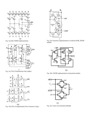
A.Presented Full Adder:
This full adder uses 16 transistors with the delay of 61.4ps and
power consumption is 2.94μW. It has a good voltage swing
maintained in the output.
The efficient coupling of strong transmission gates driven by
weak CMOS inverters leads to fast switching speeds (61.4 ps
at 1.8-V supply). This circuit shows the proper result for 0.9v
with power dissipation of 818.2nW, for 1.2V supply, the
power dissipation is 1.456μW.
B.14-Transistor Full Adder:
This uses 14 transistors for the implementation of hybrid full
adder, This is implemented using pass transistor logic and
transmission gates. It has a good logic swing but it has added
noise to it.
C. HPSC
This is a hybrid pass logic with static CMOS output drive full
adder. This is implemented using 22 transistors. It gives
proper voltage swing, but because of more area consumption
and more delay this is not preferred. The driving capability of
this hybrid adder is less when cascaded. So, proper buffers are
supposed to be used.
IV. SIMULATION RESULTS AT DIFFERENT VOLTAGE LEVELS:
At 1.8V DC supply:
At 0.9 V DC Voltage supply
At 1.2 V DC Voltage supply
V. CONCLUSION
In this paper, hybrid design for the 1-bit full adder has been
proposed. Comparison between different logic styles and
different hybrid full adders is made in terms of performance
parameters like power, delay. And the simulation is also
carried out. In these weak (channel width of transistor is
reduced) inverters has been coupled with strong (channel
width of transistor is increased) transmission gates in order to
decrease the power consumption and the delay. XOR-XNOR
contributes to the major power loss in the circuit, so the width
is reduced to the maximum possible extent to reduce
capacitance which reduces the power. By increasing the size
of transistors in the transmission gate the delay is reduced.
Simulation is carried out using Cadence Virtuoso tool in 180-
nm technology. Simulation is carried out at 1.8V, 1.2V and
0.9V; this gives the power consumption of 2.94μW, 1.456μW
and 818.2nW respectively and the delay of 61.4ps, 112.7ps,
154.6ps respectively. With this it is very evident that by using
the hybrid adder power efficient adder can be proposed.
REFERENCES
[1] N. H. E. Weste, D. Harris, and A. Banerjee, CMOS VLSI
Design:A Circuits and Systems Perspective, 3rd ed. Delhi,
India: Pearson Education, 2006.
[2] M. Vesterbacka, “A 14-transistor CMOS full adder with
full voltageswing nodes,” in Proc. IEEE Workshop Signal
Process. Syst. (SiPS), Taipei, Taiwan, Oct. 1999, pp. 713–722.](https://image.slidesharecdn.com/4d1c5999-a041-4851-a86e-ec9cddbf778a-160614060459/85/ha_report-modified-5-320.jpg)
![[3] M. Zhang, J. Gu, and C.-H. Chang, “A novel hybrid pass
logic with static CMOS output drive full-adder cell,” in Proc.
Int. Symp. Circuits Syst., May 2003, pp. 317–320.
[4] S. Goel, M. Elgamel, and M. A. Bayoumi, “Novel design
methodology for high-performance XOR-XNOR circuit
design,” in Proc. 16th Symp.Integr. Circuits Syst. Design
(SBCCI), Sep. 2003, pp. 71–76.
[5] S. Goel, A. Kumar, and M. A. Bayoumi, “Design of
robust, energyefficient full adders for deep-submicrometer
design using hybrid-CMOS logic style,” IEEE Trans. Very
Large Scale Integr. (VLSI) Syst., vol. 14,no. 12, pp. 1309–
1321, Dec. 2006.
[6] J.-M. Wang, S.-C. Fang, and W.-S. Feng, “New efficient
designs for XOR and XNOR functions on the transistor level,”
IEEE J. Solid-State Circuits, vol. 29, no. 7, pp. 780–786, Jul.
1994.
[7] M. J. Zavarei, M. R. Baghbanmanesh, E. Kargaran, H.
Nabovati, and A. Golmakani, “Design of new full adder cell
using hybrid-CMOS logic style,” in Proc. 18th IEEE Int.
Conf. Electron., Circuits Syst. (ICECS), Dec. 2011, pp. 451–
454.
[8] M. Aguirre-Hernandez and M. Linares-Aranda, “CMOS
full-adders for energy-efficient arithmetic applications,” IEEE
Trans. Very Large Scale Integr. (VLSI) Syst., vol. 19, no. 4,
pp. 718–721, Apr. 2011.
[9] M. Alioto, G. Di Cataldo, and G. Palumbo, “Mixed full
adder topologies for high-performance low-power arithmetic
circuits,” Microelectron. J., vol. 38, no. 1, pp. 130–139, Jan.
2007.](https://image.slidesharecdn.com/4d1c5999-a041-4851-a86e-ec9cddbf778a-160614060459/85/ha_report-modified-6-320.jpg)


![[IJCT-V3I2P23] Authors: Baljinder Kaur, Narinder Sharma](https://cdn.slidesharecdn.com/ss_thumbnails/ijct-v3i2p23-160609062619-thumbnail.jpg?width=640&height=640&fit=bounds)


