This document summarizes the design of a high-frequency field-programmable analog array (FPAA). Key points:
- The FPAA architecture is based on a regular pattern of identical cells that are locally interconnected for high frequency performance. Programming is achieved by modifying cells' bias conditions digitally, not via switches in the signal path.
- Each cell can perform functions like weighted summing, multiplication, integration, and nonlinear operations like clipping. Cells operate in either a passive mode where analog blocks process signals, or an active mode where a control block provides additional nonlinear functions.
- The locally interconnected architecture restricts connections between cells to improve high frequency performance, while still supporting implementation of classes of circuits like filters
This document summarizes a research paper that proposes a new routing algorithm for mobile ad hoc networks using fuzzy logic. The algorithm considers three input variables - signal power, mobility, and delay. It defines fuzzy sets and membership functions to map crisp normalized values of these variables to linguistic values. Rules are written to relate the input and output linguistic variables. The output represents the optimal route. The algorithm aims to address routing problems related to bandwidth, signal power, mobility, and delay in a distributed manner without relying on centralized control. It is designed to quickly adapt to changes in network topology.
IJERA (International journal of Engineering Research and Applications) is International online, ... peer reviewed journal. For more detail or submit your article, please visit www.ijera.com
Simulation Based Routing Protocols Evaluation for IEEE 802.15.4 enabled Wirel...IDES Editor
Wireless sensor network (WSN) is emerging as a
major research field in computer networks over the last decade
due to its wide variety of embedded real time applications.
Sensor networks have infrastructure-less architecture because
of frequently varying topology and link status. Routing is an
extremely challenging task for battery-powered resourceconstrained
WSN, since it is main cause for energy depletion
and energy must be utilized prudently to enhance lifetime
for sensor networks. This drives a myriad of research efforts
aiming at efficient data dissemination. In this paper we
analyze how efficiently MANET specific routing protocols
OLSR (Optimized Link-State Routing protocol), DYMO
(Dynamic MANET On-demand) and ZRP (Zone Routing
Protocol) perform in IEEE 802.15.4 enabled wireless sensor
networks and evaluate their simulation results using Qualnet
simulator. Several simulations were carried out under varying
network size and offered load for performance evaluation and
relative comparison of protocols is reported in terms of average
end to end delay, throughput and jitter.
EFFECTS OF MAC PARAMETERS ON THE PERFORMANCE OF IEEE 802.11 DCF IN NS-3ijwmn
This paper presents the design procedure of the NS-3 script for WLAN that is organized according to the hierarchical manner of TCP/IP model. We configure all layers by using NS-3 model objects and set and modify the values used by objects to investigate the effects of MAC parameters (access mechanism, CWmin, CWmax and retry limit) on the performance metrics viz. packet delivery ratio, packet lost ratio, aggregated throughput, and average delay. The simulation results show that RTS/CTS access mechanism outperforms basic access mechanism in saturated state, whereas the MAC parameters have no significant impact on network performance in non-saturated state. A higher value of CWmin improves the aggregated throughput in expense of average delay. The tradeoff relationships among the performance metrics are also observed in results for the optimal values of MAC parameters. Our design procedure represents a good guideline for new NS-3 users to design and modify script and results greatly benefit the network design and management.
Network on Chip Architecture and Routing Techniques: A surveyIJRES Journal
This document summarizes research on Network on Chip (NOC) architecture and routing techniques. It discusses NOC topology options including mesh, torus, ring and irregular networks. It also reviews router architecture, switching techniques, virtual channels, buffering, error correction, quality of service implementations, and routing algorithms. Specific NOC implementations discussed include QNOC, Ethereal NOC, and SPIN NOC. The document provides an overview of research on improving performance and efficiency in NOC design.
A swarm intelligence-based unicast routing protocol for hybrid ad hoc networksMarc Manthey
We present a hybrid routing protocol for both pure and hybrid ad hoc networks which uses the mechanisms of swarm
intelligence to select next hops. Our protocol, Ad hoc Networking with Swarm Intelligence (ANSI), is a congestion-aware
routing protocol, which, owing to the self-organizing mechanisms of swarm intelligence, is able to collect more information
about the local network and make more effective routing decisions than traditional MANET protocols.
Priority based bandwidth allocation in wireless sensor networksIJCNCJournal
Most of the sensor network applications need real time communication and the need for deadline aware real time communication is becoming eminent in these applications. These applications have different dead line requirements also. The real time applications of wireless sensor networks are bandwidth sensitive and need higher share of bandwidth for higher priority data to meet the dead line requirements. In this paper we focus on the MAC layer modifications to meet the real time requirements of different priority data.Bandwidth partitioning among different priority transmissions is implemented through MAC layer modifications. The MAC layer implements a queuing model that supports lower transfer rate for lower
priority packets and higher transfer rate for real
time packets with higher priority, minimizing the end to
end delay. The performance of the algorithm is evaluated with varying node distribution
.
IRJET - Improving Energy Efficiency for EMRP Routing Protocol for Virtualizat...IRJET Journal
The document proposes a new routing protocol called Optimal, Adaptive and Energy driven Mesh Routing Protocol (OAEMRP) for virtualized wireless sensor networks (VSNs). OAEMRP aims to reduce energy consumption and improve network lifetime compared to existing protocols like newEMRP. It does this by limiting the number of broadcast messages during relay node selection and giving equal weight to factors like energy, distance, and angle when choosing relay paths. Simulation results show OAEMRP achieves lower energy consumption, longer network lifetime, and lower packet loss than newEMRP and other similar protocols.
Noise Tolerant and Faster On Chip Communication Using Binoc ModelIJMER
International Journal of Modern Engineering Research (IJMER) is Peer reviewed, online Journal. It serves as an international archival forum of scholarly research related to engineering and science education.
TERNARY TREE ASYNCHRONOUS INTERCONNECT NETWORK FOR GALS’ SOCVLSICS Design
Interconnect fabric requires easy integration of computational block operating with unrelated clocks. This paper presents asynchronous interconnect with ternary tree asynchronous network for Globally Asynchronous Locally Synchronous (GALS) system-on-chip (SOC). Here architecture is proposed for interconnection with ternary tree asynchronous network where ratio of number NOC design unit and number of router is 4:1,6:2, 8:3,10:4 etc .It is scalable for any number of NOC design unit. It offers an easy integration of different clock domain with low communication overhead .NOC design unit for GALS ‘SOC is formulated by wrapping synchronous module with input port along with input port controller, output port along with output port controller and local clock generator. It creates the interface between synchronous to asynchronous and asynchronous to synchronous. For this purpose four port asynchronous routers is designed with routing element and output arbitration and buffering with micro-pipeline. This interconnect fabric minimizes silicon area, minimize Latency and maximize throughput. Here functional model is made for TTAN and application MPEG4 is mapped on the Network .Desired traffic pattern is generated and performance of the network is evaluated. Significant improvement in the network performance parameter has been observed.
PERFORMANCE ANALYSIS OF CHANNEL ACCESS MODEL FOR MAC IN RANDOMLY DISTRIBUTED ...IJCNCJournal
Medium Access control (MAC) is one of the fundamental problems in wireless sensor networks. The performance of wireless sensor network depends on it. The main objective of a medium access control method is to provide high throughput, minimize the delay, and conservers the energy consumption by avoiding the collisions. In this paper, a general model for MAC protocol to reduce the delay, maximize throughput and conserve the energy consumption in channel accessing in high density randomly distributed wireless sensor network is presented. The proposed model is simulated using MATLAB. The simulation results show that the average delay for sensors with sufficient memory is lower than sensors without
memory. Further, the throughput of the channel access method with memory is better than without memory.
Traffic engineering is one of the major issues that has to be addressed in Metro Ethernet networks for quality of service and efficient resource utilization. This paper aims at understanding the relevant issues and outlines novel algorithms for multipoint traffic engineering in Metro Ethernet. We present an algorithmic solution for traffic engineering in Metro Ethernet using optimal multiple spanning trees. This iterative approach distributes traffic across the network uniformly without overloading network resources. We also introduce a new traffic specification model for Metro Ethernet, which is a hybrid of two widely used traffic specification models, the pipe and hose models.
Energy Minimization in Wireless Sensor Networks Using Multi Hop TransmissionIOSR Journals
This document discusses energy minimization in wireless sensor networks using multi-hop transmissions. It provides background on wireless sensor networks and their components. It then discusses challenges like limited energy and the need for multi-hop transmissions due to limited transmission range. The document outlines the problem of determining the optimal number of cooperating nodes per hop to minimize total energy consumption while meeting an outage probability requirement at each hop. It discusses using cooperative transmissions to increase transmission range through diversity gain while keeping transmit power fixed.
This document describes a dynamic topology switch that was developed to emulate wireless mobile ad hoc networks. The switch connects multiple hosts according to a controllable dynamic topology and bit error rate on the links. This allows researchers to experiment with routing and other protocols in a mobile ad hoc network environment without needing to deploy a real wireless testbed. The switch is implemented in Linux and uses standard Ethernet connections, requiring no changes to the network hosts. It was validated by comparing control packet overhead measurements using the switch to those from the ns-2 network simulator for the OLSR routing protocol.
Emerging Technologies in On-Chip and Off-Chip Interconnection NetworksAshif Sikder
This document proposes emerging technologies for on-chip and off-chip interconnection networks, including optical network-on-chip (OWN) and reconfigurable optical and wireless network-on-chip (R-OWN). OWN combines optical and wireless interconnects to overcome limitations of each individually. R-OWN extends OWN with reconfigurable wireless links to improve utilization and throughput. Simulations show OWN and R-OWN reduce area, energy, latency and improve throughput compared to wired-only and hybrid wireless baselines.
The document discusses different network topologies including star, bus, ring, tree, graph, and mesh. It provides details on the key characteristics of each topology such as the pattern of interconnection between nodes and examples of common uses. The advantages and disadvantages of each topology are also summarized.
Active path updation for layered routing (apular) in wirelessAlexander Decker
1) The document proposes an Active Path Updation procedure (APULAR) for layered routing in wireless mesh networks to quickly update broken paths and reduce packet loss.
2) In APULAR, the destination node takes responsibility for local repair restoration instead of the source node initiating a new path discovery when a link breaks, as is typically done.
3) The procedure is simulated and shown to outperform AODV and IWMRA routing protocols, achieving better packet delivery ratio, lower control overhead, higher throughput, and lower end-to-end delay.
Network on a chip is an approach where the communication features of large-scale integrated systems are implemented on a single silicon chip. It reduces complexity in wiring design and provides better power, speed and reliability compared to other designs. Network on a chip uses switches and links to route messages from source to destination modules in a scalable, homogeneous switched fabric network. It improves power efficiency and allows for features like multi-topology support in complex system-on-chip designs.
Design and Performance Analysis of Energy Aware Routing Protocol for Delay Se...ijcncs
This document presents a study on an energy aware routing protocol called Energy Aware DSR (EADSR) for wireless sensor networks. EADSR is an extension of the Dynamic Source Routing (DSR) protocol that adds energy awareness to improve network lifetime. The study compares the performance of DSR and EADSR through simulations. Results show that EADSR outperforms DSR in terms of energy savings and avoids early network partitioning caused by nodes draining their energy quickly. EADSR selects routes based on the total energy of nodes along the path and notifies neighbors when a node's energy is low to find alternative routes before it fails.
This document provides an introduction and overview of mobile ad hoc networks (MANETs). It discusses how MANETs are self-configuring networks formed by mobile nodes without a fixed infrastructure. The key characteristics of MANETs include using wireless communication, nodes acting as both hosts and routers, limited bandwidth and variable capacity links, energy-constrained operation, and dynamic network topology. The document also outlines some common applications of MANETs and provides an overview of different routing protocols used in MANETs, including proactive, reactive, and hybrid protocols. It gives a brief description of distance-vector and link-state routing approaches.
Ijeee 24-27-energy efficient communication for adhoc networksKumar Goud
Energy Efficient Communication for Adhoc Networks
1SK.Nagula Meera 2Dr. D.Srinivasa Kumar 3Dr. D.Srinivasa Rao
Research Scholar Professor & Principal Professor, ECE department
ECE department, JNTU Hyderabad Hosur Institute of Technology and Science
Errandapalli Village, Beerpalli PO JNTU College of Engineering Hyderabad(Autonomous)
Ramapuram (via), Krishnagri Dt., Tamilnadu
Abstract: A mobile accidental network (MANET) may be an assortment of nodes equipped with wireless communications and a networking capability while not central network management. The method of wireless networks within the applications like transferring video files is subjected to twin constraints. Each step-down of power and different QOS needs like delay, throughputs square measure need to be bewaring properly. Mobile accidental Networks square measure a lot of perceptive to those problems wherever every mobile device is active sort of a router and consequently, routing delay adds significantly to overall end-to-end delay. This paper presents a survey on power economical routing protocols for Mobile Ad-Hoc Networks. This survey focused on recent progress on power saving algorithms. Additionally we recommend one power aware technique which can cut back power consumption yet as increase the lifespan of node and network.
Keywords: Mobile, Ad-Hoc networks, QOS, MANET, IBSS, ATIM, DPSM.
Comparative Simulation Study Of LEACH-Like And HEED-Like Protocols Deployed I...IOSRJECE
WSNs represents one of the most interesting research areas with deep impact on technological development because of their potential usage in a wide variety of applications such as fire monitoring, border surveillance medical care, and highway traffic coordination. Therefore, WSNs researchers have defined many routing protocols for this type of network. In this paper, we have implemented and analyzed different clustering protocols, namely LEACH, LEACH-C, LEACH-1R, and HEED using MATLAB environment. These routing protocols are compared in different terms such as residual energy, data delivery to the base station, number of rounds and live nodes
Comparative Review for Routing Protocols in Mobile Ad-Hoc Networksijasuc
Wireless Mobile Ad-Hoc Networks is one of the attractive research field that growing exponentially in the
last decade. it surrounded by much challenges that should be solved the improve establishment of such
networks. Failure of wireless link is considered as one of popular challenges faced by Mobile Ad-Hoc
Networks (MANETs). As this type of networks does not require any pre-exist hardware. As well as, every
node have the ability of roaming where it can be connected to other nodes dynamically. Therefore, the
network internal structure will be unpredictably changed frequently according to continuous activities
between nodes that simultaneously update network topology in the basis of active ad-hoc nature. This
model puts the functionality of routing operation in crucial angle in the area of research under mobile adhoc
network field due to highly dynamic nature. Adapting such kernel makes MANET indigence new
routing techniques to settle these challenges. Thereafter, tremendous amount of routing protocols proposed
to argue with ad-hoc nature. Thus, it is quite difficult to specify which protocols operate efficiently under
different mobile ad-hoc scenarios. This paper examines some of the prominent routing protocols that are
designed for mobile ad-hoc networks by describing their structures, operations, features and then
comparing their various characteristics.
DYNAMIC HYBRID CHANNEL (WMN) FOR BANDWIDTH GUARANTEES IN AD_HOC NETWORKSpharmaindexing
This document discusses bandwidth guarantees in wireless mesh networks. It proposes a new routing technique called dynamic hybrid channel, which uses both proactive and reactive routing protocols based on AOMDV. The goal is to provide bandwidth guarantees by selecting multiple paths and using the path with the highest available bandwidth for transmission. The performance of this approach is evaluated using the NS-2 network simulator. Several challenges of wireless mesh networks are also discussed, such as interference reduction and improving throughput across multiple hops.
Power Optimization Technique for Sensor NetworkEditor IJCATR
In this paper different power optimization techniques for wireless sensor network is proposed and compared. The
energy conservation in a wireless sensor network is of great significance and very essential. The nodes in a wireless environment are
subject to less transmission capabilities and limited battery resources. There are several issues that constrain the WSNs and challenges
posed by the environment of handling traffic and the lifetime of the battery in the nodes. The battery of node is energy limited and is
not convenient to be replaced by the restriction of circumstance. But we have to ensure that even the slightest of energy is utilized and
the overall power conserved in a wireless environment is greatly reduced. This paper aims to reduce the power conservation in a
wireless sensor network using Dijkstra‘s algorithm, with a set of optimal path and available idle nodes.
A New Approach to Improve the Efficiency of Distributed Scheduling in IEEE 80...IDES Editor
The recent standard for broadband wireless
access networks, IEEE 802.16, which resulted in the
development of metropolitan area wireless networks,
includes two network organization modes: Point to Multi
Point and Mesh. The mesh mode provides distributed
channel access operations of peering nodes and uses TDMA
technique for channel access modulation. According to
IEEE 802.16 MAC protocol, there are two scheduling
algorithms for assigning TDMA slots to each network node:
centralized and distributed. In distributed scheduling
algorithm, network nodes have to transmit scheduling
message in order to inform other nodes about their transfer
schedule. In this paper a new approach is proposed to
improve distributed scheduling efficiency in IEEE 802.16
mesh mode, with respect to network condition in every
transferring opportunity. For evaluating the proposed
algorithm efficiency, several extensive simulations are
performed in various network configurations and the most
important system parameters which affect the network
performance are analyzed.
IEEE JOURNAL OF SOLID-STATE CIRCUITS, VOL. 32, NO. 7, JULY 199MalikPinckney86
IEEE JOURNAL OF SOLID-STATE CIRCUITS, VOL. 32, NO. 7, JULY 1997 1079
Low-Power Logic Styles: CMOS
Versus Pass-Transistor Logic
Reto Zimmermann and Wolfgang Fichtner,Fellow, IEEE
Abstract—Recently reported logic style comparisons based on
full-adder circuits claimed complementary pass-transistor logic
(CPL) to be much more power-efficient than complementary
CMOS. However, new comparisons performed on more efficient
CMOS circuit realizations and a wider range of different logic
cells, as well as the use of realistic circuit arrangements demon-
strate CMOS to be superior to CPL in most cases with respect
to speed, area, power dissipation, and power-delay products.
An implemented 32-b adder using complementary CMOS has
a power-delay product of less than half that of the CPL version.
Robustness with respect to voltage scaling and transistor sizing,
as well as generality and ease-of-use, are additional advantages
of CMOS logic gates, especially when cell-based design and logic
synthesis are targeted. This paper shows that complementary
CMOS is the logic style of choice for the implementation of
arbitrary combinational circuits if low voltage, low power, and
small power-delay products are of concern.
Index Terms—Adder circuits, CPL, complementary CMOS,
low-voltage low-power logic styles, pass-transistor logic, VLSI
circuit design.
I. I NTRODUCTION
T HE increasing demand for low-power very large scaleintegration (VLSI) can be addressed at different de-
sign levels, such as the architectural, circuit, layout, and
the process technology level [1]. At the circuit design level,
considerable potential for power savings exists by means of
proper choice of a logic style for implementing combinational
circuits. This is because all the important parameters governing
power dissipation—switching capacitance, transition activity,
and short-circuit currents—are strongly influenced by the
chosen logic style. Depending on the application, the kind
of circuit to be implemented, and the design technique used,
different performance aspects become important, disallowing
the formulation of universal rules for optimal logic styles. In-
vestigations of low-power logic styles reported in the literature
so far, however, have mainly focused on particular logic cells,
namely full-adders, used in some arithmetic circuits. In this
paper, these investigations are extended to a much wider set of
logic gates, and with that, to arbitrary combinational circuits.
The power dissipation characteristics of various existing logic
styles are compared qualitatively and quantitatively by actual
logic gate implementations and simulations under realistic cir-
cuit arrangements and operating conditions [2]. Investigations
of sequential elements, such as latches and flip-flops, were
Manuscript received November 20, 1996; revised January 29, 1997.
The authors are with the Integrated Systems Laboratory, Swiss Federal
Institute of Technology (ETH), CH-8092 Zurich, Switzerland.
Publisher It ...
Open Source SDR Frontend and Measurements for 60-GHz Wireless ExperimentationAndreaDriutti
Summary of Open Source SDR Frontend and Measurements for 60-GHz Wireless Experimentation
Tesi fast track, laurea triennale Ingegneria Elettronica e Informatica.
DESIGN OF A LOW POWER MULTIBAND CLOCK DISTRIBUTION CIRCUIT USING SINGLE PHASE...IJERA Editor
The clock distribution network consumes nearly 70% of the total power consumed by the integrated circuit since
this is the only signal which has the highest switching activity. Normally for a multiband clock domain network
we develop a multiple PLL to cater the need. This project aim for developing a low power true single phase
clock(TSPC) multiband network which will supply for the multi clock domain network. In this paper, a wide
band 2/3 prescaler is verified in the design of proposed wide band multimodulus 32/33/47/48 or 64/65/78/79
prescaler. A dynamic logic multiband flexible integer-n divider based on pulse swallow topology is proposed
which uses a low power wide band 2/3 prescaler and a wide band multimodulus 32/33/47/48 or 64/65/78/79
prescaler. Since the multimodulus 32/33/47/48 or 64/65/78/79 prescaler has a maximum operating frequency of
6.2GHz, the values of P and S counters can actually be programmed to divide over the whole range of
frequencies. However the P and S counter are programmed accordingly. The proposed multiband flexible
divider also uses an improved loadable bit cell for swallow counter and consumes a power of 0.96 and 2.2mW.
This project is highly useful and recommended for communication applications like Bluetooth, Zigbee, IEEE
802.15.4 and 802.11 a/b/g WLAN frequency synthesizers which are proposed based on pulse swallow topology.
This design is modelled using Verilog simulated tool „MODELSIM 6.4b‟ and implemented and synthesized
using „Xilinx ISE 10.1‟.
Iaetsd design of a low power multiband clock distribution circuitIaetsd Iaetsd
This document describes the design of a low power multiband clock distribution circuit using a single phase clock. It proposes a dynamic logic divider based on pulse swallow topology that uses a low power 2/3 prescaler and multimodulus 32/33/47/48 prescaler. The divider allows programming to divide over a wide range of frequencies for applications like Bluetooth, Zigbee, and WiFi. It is modeled in Verilog and implemented using Xilinx tools with a power consumption of 0.96-2.2mW.
OPTIMIZATION TECHNIQUES FOR SOURCE FOLLOWER BASED TRACK-AND-HOLD CIRCUIT FOR ...VLSICS Design
Since the current demand for high-resolution and fast analog to digital converters (ADC) is driving the need for track and hold amplifiers (T&H) operating at RF frequencies. A very fast and linear T&H circuit is the key element in any modern wideband data acquisition system. Applications like a cable TV or a broad variety of different radio standards require high processing speeds with high resolution. The track-and-hold (T&H) circuit is a fundamental block for analog-to digital (A/D) converters. Its use allows most dynamic errors of A/D converters to be reduced, especially those showing up when using high frequency input signals. Having a wideband and precise acquisition system is a prerequisite for today’s trend towards multi-standard flexible radios, with as much signal processing as possible in digital domain. This work investigates effect of various design schemes and circuit topology for track
and-hold circuit to achieve acceptable linearly, high slew rate, low power consumption and low noise
Congestion Control in Wireless Sensor Networks: A surveyIJERA Editor
Congestion is a major problem in almost all kinds of wireless networks such as mobile ad-hoc networks; wireless
sensor networks (WSNs). There are variety of applications of WSN such as defense, temperature monitoring,
health monitoring. Congestion occurs in the sensor network because of limited resources such as low processing
power of the sensor node. As all the sensor nodes are battery powered. Hence, congestion in the sensor network
results in waste of energy of sensor nodes. All the layers of protocol suite of the network can be involved in the
congestion control process. This paper gives a brief idea about various congestion control methods. In some of
the schemes, cross-layer design is applied for better results.
AREA EFFICIENT 3.3GHZ PHASE LOCKED LOOP WITH FOUR MULTIPLE OUTPUT USING 45NM ...VLSICS Design
This paper present area efficient layout designs for 3.3GigaHertz (GHz) Phase Locked loop (PLL) with four multiple output. Effort has been taken to design Low Power Phase locked loop with multiple output, using VLSI technology. VLSI Technology includes process design, trends, chip fabrication, real circuit parameters, circuit design, electrical characteristics, configuration building blocks, switching circuitry, translation onto silicon, CAD and practical experience in layout design. The proposed PLL is designed using 45 nm CMOS/VLSI technology with microwind 3.1. This software allows designing and simulating an integrated circuit at physical description level. The main novelties related to the 45 nm technology are the high-k gate oxide, metal gate and very low-k interconnect dielectric. The effective gate length required for 45 nm technology is 25nm. Low Power (0.211miliwatt) phase locked loop with four multiple outputs as PLL8x, PLL4x, PLL2x, & PLL1x of 3.3 GHz, 1.65 GHz, 0.825 GHz, and 0.412 GHz respectively is obtained using 45 nm VLSI technology.
OPTICAL SWITCHING CONTROLLER USING FPGA AS A CONTROLLER FOR OCDMA ENCODER SYSTEMEditor IJCATR
This paper proposed a design of optical switching controller using FPGA for OCDMA encoder system. The encoder is one
of the new technologies that use to transmit the coded data in the optical communication system by using FPGA and optical switches.
It is providing a high security for data transmission due to all data will be transmitting in binary code form. The output signals from
FPGA are coded with a binary code that given to an optical switch before it signal modulate with the carrier and transmit to the
receiver. In this paper, AA and 55 data were used for source 1 and source 2. It is generated sample data and sent packet data to the
FPGA and stored it into RAM. The simulation results have done by using software Verilog Spartan 2 programming to simulate. After
that the output will produces at waveform to display the output. The main function of FPGA controlling unit is producing single pulse
and configuring optical switching system.
This document summarizes research on topology control techniques in wireless sensor networks. It first discusses how topology control aims to reduce energy consumption while maintaining network connectivity by regulating nodes' transmission power. It then reviews several existing topology control algorithms proposed in other papers. These algorithms distribute transmission power control to maximize network lifetime. Finally, the document concludes that many topology control algorithms have been developed to achieve energy efficient routing, but implementing them on real-world testbeds poses challenges.
IJERA (International journal of Engineering Research and Applications) is International online, ... peer reviewed journal. For more detail or submit your article, please visit www.ijera.com
International Journal of Engineering Research and Applications (IJERA) is an open access online peer reviewed international journal that publishes research and review articles in the fields of Computer Science, Neural Networks, Electrical Engineering, Software Engineering, Information Technology, Mechanical Engineering, Chemical Engineering, Plastic Engineering, Food Technology, Textile Engineering, Nano Technology & science, Power Electronics, Electronics & Communication Engineering, Computational mathematics, Image processing, Civil Engineering, Structural Engineering, Environmental Engineering, VLSI Testing & Low Power VLSI Design etc.
The document proposes a resource allocation strategy using optimal power control to mitigate interference in heterogeneous networks. It presents a system model where macrocells and femtocells are deployed. Users are divided into cell center and cell edge groups. A soft fractional frequency reuse scheme is used to improve cell edge performance. Simulations show the proposed approach improves coverage probability and SINR compared to other schemes, especially for cell edge users.
Dynamic bandwidth allocation scheme in lr pon with performance modelling and ...IJCNCJournal
We consider models of telecommunication systems that incorporate probability, dense real-time and data.
We present a new formal abstraction method for computing minimum and maximum reachability
probabilities for such models. Our approach uses strictly local formal abstract steps to reduce both the size
of abstract specifications generated and the complexity of operations needed, in comparison to previous
approaches of this kind. A selection of large case studies are implemented the techniques and evaluate,
which include some infinite-state probabilistic real time models, demonstrating improvements over existing
tools in several cases. The capacity of metro and access networks are extended the reach and split ratio of
the conventional Long - Reach Passive Optical Networks (LR-PONs). The efficient solutions of LR-PONs
are appeared in feeder distances around 100km and high split ratios up to 1000-way . Among many
existing approaches, one of the most effective options to improve network performance in LR-PONs are the
multi-thread based dynamic bandwidth allocation (DBA) scheme where several bandwidth allocation
processes are performed in parallel is considered. Without proper intercommunication between the
overlapped threads, multi-thread DBA may lose efficiency and even perform worse than the conventional
single thread algorithm. Real Time Probabilistic Systems are used to evaluate a typical PON systems
performance. This approach is more convenient, flexible, and lower cost than the former simulation method,
which do not need develop special hardware and software tools. Moreover, how changes in performance
depend on changes in the particular modes can be easily analysis by supplying ranges for parameter values.
The proposed algorithm with traditional DBA is compared, and shows its advantage on average packet
delay. The key parameters of the algorithm are analysed and optimized, such as initiating and tuning
multiple threads, inter -thread scheduling, and fairness among users. The algorithms advantage in
numerical results are decreased the average packet delay and improve network throughput under varying
offered loads.
This document summarizes research on improving the capacity of cellular systems using fractional frequency reuse (FFR). It discusses how frequency reuse is used to increase the number of users that can be served but causes interference, particularly for cell edge users. Fractional frequency reuse is proposed to solve this problem by allocating different frequency sets to cell center and edge users to reduce interference. The document also reviews different types of interference (co-channel and adjacent channel) and how power control can help reduce interference in cellular systems.
Capacity Improvement of Cellular System Using Fractional Frequency Reuse (FFR)IJEEE
Today wireless communication is mostly used rather than wired communication, due to remote location reach ability, less fault occurrence, less time to commissioning and low cost etc. But wireless network has less frequency spectrum to cover the whole world. To improve the capacity of cellular system in a limited spectrum without major technological changes, frequency is reused in cells. But it offers interferences mostly for cell edge users. To solve the problem of spectral congestion and user capacity, fractional frequency reuse is used. This paper gives idea about different frequency reuse factors, fractional frequency reuse and super cell with sectoring to improve the capacity of cellular system.
This document summarizes the design of a wireless cortical neural recording system with bidirectional data transmission. It includes:
1) The development of a transcutaneous two-way wireless power and data link for neural recording, with wireless powering at 1.25Mbps and reverse telemetry from the implant at rates over 3Mbps to stream 16 channels of raw neural data.
2) The use of an integer-N PLL in the implant circuitry to generate the reverse telemetry carrier frequency as a multiple of the power carrier frequency, allowing simultaneous reverse telemetry from multiple implants.
3) Optimization of the dual inductive link design for power transmission and reverse telemetry using an analytic model to maximize coupling between the data coils within
A Bus Encoding Method for Crosstalk and Power Reduction in RC Coupled VLSI In...VLSICS Design
The performance factors such as propagation delay, power dissipation and crosstalk in RC modelled interconnects are major design issues for the System on-chip (SoC) designs in current Deep Submicron (DSM) era. The crosstalk effect is a consequence of coupling and switching activities that is encountered when there is a transition as compared to previous state of wire and or when there are transitions in adjacent wires. Therefore, minimization or elimination of switching and coupling activities is crucial in enhancing the performance of SoC designs. There are several methods for the reduction of power dissipation, crosstalk and delay. The encoding method is most effective and popular method for enhancing the behaviour of on-chip buses. This paper proposes encoding scheme to achieve overall reduction in transitions. The reduction in transition improves the performance in terms of reduced power dissipation, coupling activity and delay in on-chip buses. This encoding method is implemented using VHDL. The result evidently demonstrates reduction in transitions which consequently improves the overall performance of on-chip buses.
IRJET- An Evaluation of the Performance Parameters of CMOS and CNTFET based D...IRJET Journal
The document compares the performance parameters of CMOS and carbon nanotube field-effect transistor (CNTFET) based delay lines at a 32nm technology node. A simulation study found that CNTFET delay lines exhibited improved results over CMOS for parameters like propagation delay, leakage power, and leakage current. Specifically, leakage power decreased and average power consumption was lower in CNTFET delay lines. So CNTFETs showed better evaluation and performance metrics than CMOS for delay lines.
This document proposes two novel beamforming methodologies that employ passive RF devices to enhance received signal strength through passive, scattering-based beamforming. It develops models to describe RF signal propagation between nodes in the presence of scattering devices. It also formulates the problem of selecting devices to maximize received power at the destination node. Two distributed beamforming algorithms are proposed - one based on Taguchi methods and one using learning automata - to identify suitable scattering devices without requiring precise timing synchronization. Simulation results show the proposed approaches can achieve power improvements over line-of-sight signals of 37.5dB and 33dB, respectively, for a 100-device network.
Full-RAG: A modern architecture for hyper-personalizationZilliz
Mike Del Balso, CEO & Co-Founder at Tecton, presents "Full RAG," a novel approach to AI recommendation systems, aiming to push beyond the limitations of traditional models through a deep integration of contextual insights and real-time data, leveraging the Retrieval-Augmented Generation architecture. This talk will outline Full RAG's potential to significantly enhance personalization, address engineering challenges such as data management and model training, and introduce data enrichment with reranking as a key solution. Attendees will gain crucial insights into the importance of hyperpersonalization in AI, the capabilities of Full RAG for advanced personalization, and strategies for managing complex data integrations for deploying cutting-edge AI solutions.
Infrastructure Challenges in Scaling RAG with Custom AI modelsZilliz
Building Retrieval-Augmented Generation (RAG) systems with open-source and custom AI models is a complex task. This talk explores the challenges in productionizing RAG systems, including retrieval performance, response synthesis, and evaluation. We’ll discuss how to leverage open-source models like text embeddings, language models, and custom fine-tuned models to enhance RAG performance. Additionally, we’ll cover how BentoML can help orchestrate and scale these AI components efficiently, ensuring seamless deployment and management of RAG systems in the cloud.
GraphSummit Singapore | The Future of Agility: Supercharging Digital Transfor...Neo4j
Leonard Jayamohan, Partner & Generative AI Lead, Deloitte
This keynote will reveal how Deloitte leverages Neo4j’s graph power for groundbreaking digital twin solutions, achieving a staggering 100x performance boost. Discover the essential role knowledge graphs play in successful generative AI implementations. Plus, get an exclusive look at an innovative Neo4j + Generative AI solution Deloitte is developing in-house.
AI 101: An Introduction to the Basics and Impact of Artificial IntelligenceIndexBug
Imagine a world where machines not only perform tasks but also learn, adapt, and make decisions. This is the promise of Artificial Intelligence (AI), a technology that's not just enhancing our lives but revolutionizing entire industries.
GraphSummit Singapore | The Art of the Possible with Graph - Q2 2024Neo4j
Neha Bajwa, Vice President of Product Marketing, Neo4j
Join us as we explore breakthrough innovations enabled by interconnected data and AI. Discover firsthand how organizations use relationships in data to uncover contextual insights and solve our most pressing challenges – from optimizing supply chains, detecting fraud, and improving customer experiences to accelerating drug discoveries.
For the full video of this presentation, please visit: https://www.edge-ai-vision.com/2024/06/building-and-scaling-ai-applications-with-the-nx-ai-manager-a-presentation-from-network-optix/
Robin van Emden, Senior Director of Data Science at Network Optix, presents the “Building and Scaling AI Applications with the Nx AI Manager,” tutorial at the May 2024 Embedded Vision Summit.
In this presentation, van Emden covers the basics of scaling edge AI solutions using the Nx tool kit. He emphasizes the process of developing AI models and deploying them globally. He also showcases the conversion of AI models and the creation of effective edge AI pipelines, with a focus on pre-processing, model conversion, selecting the appropriate inference engine for the target hardware and post-processing.
van Emden shows how Nx can simplify the developer’s life and facilitate a rapid transition from concept to production-ready applications.He provides valuable insights into developing scalable and efficient edge AI solutions, with a strong focus on practical implementation.
Driving Business Innovation: Latest Generative AI Advancements & Success StorySafe Software
Are you ready to revolutionize how you handle data? Join us for a webinar where we’ll bring you up to speed with the latest advancements in Generative AI technology and discover how leveraging FME with tools from giants like Google Gemini, Amazon, and Microsoft OpenAI can supercharge your workflow efficiency.
During the hour, we’ll take you through:
Guest Speaker Segment with Hannah Barrington: Dive into the world of dynamic real estate marketing with Hannah, the Marketing Manager at Workspace Group. Hear firsthand how their team generates engaging descriptions for thousands of office units by integrating diverse data sources—from PDF floorplans to web pages—using FME transformers, like OpenAIVisionConnector and AnthropicVisionConnector. This use case will show you how GenAI can streamline content creation for marketing across the board.
Ollama Use Case: Learn how Scenario Specialist Dmitri Bagh has utilized Ollama within FME to input data, create custom models, and enhance security protocols. This segment will include demos to illustrate the full capabilities of FME in AI-driven processes.
Custom AI Models: Discover how to leverage FME to build personalized AI models using your data. Whether it’s populating a model with local data for added security or integrating public AI tools, find out how FME facilitates a versatile and secure approach to AI.
We’ll wrap up with a live Q&A session where you can engage with our experts on your specific use cases, and learn more about optimizing your data workflows with AI.
This webinar is ideal for professionals seeking to harness the power of AI within their data management systems while ensuring high levels of customization and security. Whether you're a novice or an expert, gain actionable insights and strategies to elevate your data processes. Join us to see how FME and AI can revolutionize how you work with data!
“An Outlook of the Ongoing and Future Relationship between Blockchain Technologies and Process-aware Information Systems.” Invited talk at the joint workshop on Blockchain for Information Systems (BC4IS) and Blockchain for Trusted Data Sharing (B4TDS), co-located with with the 36th International Conference on Advanced Information Systems Engineering (CAiSE), 3 June 2024, Limassol, Cyprus.
Essentials of Automations: The Art of Triggers and Actions in FMESafe Software
In this second installment of our Essentials of Automations webinar series, we’ll explore the landscape of triggers and actions, guiding you through the nuances of authoring and adapting workspaces for seamless automations. Gain an understanding of the full spectrum of triggers and actions available in FME, empowering you to enhance your workspaces for efficient automation.
We’ll kick things off by showcasing the most commonly used event-based triggers, introducing you to various automation workflows like manual triggers, schedules, directory watchers, and more. Plus, see how these elements play out in real scenarios.
Whether you’re tweaking your current setup or building from the ground up, this session will arm you with the tools and insights needed to transform your FME usage into a powerhouse of productivity. Join us to discover effective strategies that simplify complex processes, enhancing your productivity and transforming your data management practices with FME. Let’s turn complexity into clarity and make your workspaces work wonders!
Building Production Ready Search Pipelines with Spark and MilvusZilliz
Spark is the widely used ETL tool for processing, indexing and ingesting data to serving stack for search. Milvus is the production-ready open-source vector database. In this talk we will show how to use Spark to process unstructured data to extract vector representations, and push the vectors to Milvus vector database for search serving.
Observability Concepts EVERY Developer Should Know -- DeveloperWeek Europe.pdfPaige Cruz
Monitoring and observability aren’t traditionally found in software curriculums and many of us cobble this knowledge together from whatever vendor or ecosystem we were first introduced to and whatever is a part of your current company’s observability stack.
While the dev and ops silo continues to crumble….many organizations still relegate monitoring & observability as the purview of ops, infra and SRE teams. This is a mistake - achieving a highly observable system requires collaboration up and down the stack.
I, a former op, would like to extend an invitation to all application developers to join the observability party will share these foundational concepts to build on:
How to Get CNIC Information System with Paksim Ga.pptxdanishmna97
Pakdata Cf is a groundbreaking system designed to streamline and facilitate access to CNIC information. This innovative platform leverages advanced technology to provide users with efficient and secure access to their CNIC details.
UiPath Test Automation using UiPath Test Suite series, part 5DianaGray10
Welcome to UiPath Test Automation using UiPath Test Suite series part 5. In this session, we will cover CI/CD with devops.
Topics covered:
CI/CD with in UiPath
End-to-end overview of CI/CD pipeline with Azure devops
Speaker:
Lyndsey Byblow, Test Suite Sales Engineer @ UiPath, Inc.
HCL Notes and Domino License Cost Reduction in the World of DLAUpanagenda
Webinar Recording: https://www.panagenda.com/webinars/hcl-notes-and-domino-license-cost-reduction-in-the-world-of-dlau/
The introduction of DLAU and the CCB & CCX licensing model caused quite a stir in the HCL community. As a Notes and Domino customer, you may have faced challenges with unexpected user counts and license costs. You probably have questions on how this new licensing approach works and how to benefit from it. Most importantly, you likely have budget constraints and want to save money where possible. Don’t worry, we can help with all of this!
We’ll show you how to fix common misconfigurations that cause higher-than-expected user counts, and how to identify accounts which you can deactivate to save money. There are also frequent patterns that can cause unnecessary cost, like using a person document instead of a mail-in for shared mailboxes. We’ll provide examples and solutions for those as well. And naturally we’ll explain the new licensing model.
Join HCL Ambassador Marc Thomas in this webinar with a special guest appearance from Franz Walder. It will give you the tools and know-how to stay on top of what is going on with Domino licensing. You will be able lower your cost through an optimized configuration and keep it low going forward.
These topics will be covered
- Reducing license cost by finding and fixing misconfigurations and superfluous accounts
- How do CCB and CCX licenses really work?
- Understanding the DLAU tool and how to best utilize it
- Tips for common problem areas, like team mailboxes, functional/test users, etc
- Practical examples and best practices to implement right away
Sudheer Mechineni, Head of Application Frameworks, Standard Chartered Bank
Discover how Standard Chartered Bank harnessed the power of Neo4j to transform complex data access challenges into a dynamic, scalable graph database solution. This keynote will cover their journey from initial adoption to deploying a fully automated, enterprise-grade causal cluster, highlighting key strategies for modelling organisational changes and ensuring robust disaster recovery. Learn how these innovations have not only enhanced Standard Chartered Bank’s data infrastructure but also positioned them as pioneers in the banking sector’s adoption of graph technology.
Best 20 SEO Techniques To Improve Website Visibility In SERPPixlogix Infotech
Boost your website's visibility with proven SEO techniques! Our latest blog dives into essential strategies to enhance your online presence, increase traffic, and rank higher on search engines. From keyword optimization to quality content creation, learn how to make your site stand out in the crowded digital landscape. Discover actionable tips and expert insights to elevate your SEO game.
Presentation of the OECD Artificial Intelligence Review of Germany
10
1. Analog Integrated Circuits and Signal Processing, 17, 143±156 (1998)
# 1998 Kluwer Academic Publishers, Boston. Manufactured in The Netherlands.
A High-Frequency Field-Programmable Analog Array (FPAA)
Part 1: Design
EDMUND PIERZCHALA AND MAREK A. PERKOWSKI
Department of Electrical Engineering, Portland State University, Portland, OR 97207-0751
edmundp@ee.pdx.edu, mperkows@ee.pdx.edu
Received August 2, 1996; Accepted November 10, 1997
Abstract. The design of a high-frequency ®eld-programmable analog array (FPAA) is presented. The FPAA is
based on a regular pattern of cells interconnected locally for high frequency performance. No switches of any kind
are used in the signal path of a cell: programming of the functions, parameters, and interconnections is achieved
solely by modifying cells' bias conditions digitally. Limited global signal interconnections are also available for
those application circuits which cannot be mapped onto locally-only interconnected structure. Key circuits of the
FPAA have been fabricated in a CPI transistor-array bipolar technology.
Key Words: programmable circuit, ®eld-programmable analog array (FPAA), current-mode circuit, analog
signal processing
1. Introduction
Field-Programmable Gate Arrays (FPGAs) have
found many applications since they were proposed
about a decade ago. FPGAs dramatically shorten
design time and allow instantaneous modi®cations
and corrections. Their applications range from simple
``glue logic'' functions to complex, dynamically
recon®gurable systems.
The success of FPGAs is undoubtedly one of
motivating factors in the FPAA research. With the
current trend which favors digital techniques, analog
circuits seem to be left to perform interface functions
(such as A/D, D/A converters, anti-alias and
smoothing ®lters) or work where digital circuits did
not yet achieve satis®able performance (e.g. high-
frequency applications). It seems that analog circuits,
as more capricious and harder to design, should yield
to digital ones. In fact, the picture is not so simple, and
the ``digital revolution'' relies heavily on progress in
analog circuits in each of its victories [21]. The design
complexity of analog front-end and back-end circuits
may exceed the complexity of the digital signal
processing circuit they work with. As an example one
can consider processing of video signals, or any other
signals of suf®ciently high bandwidth. In such
applications, the sampling frequency is often chosen
to be close to the Nyquist frequency, which poses
stringent requirements on the anti-aliasing ®lter
design, leading to high-order ®lters. Moreover, if
high linearity and low noise are desired, one must not
only assure high quality of data converters, but also
the analog front and back ends. All in all, the analog
part of the entire system may easily become as or even
more complex than the digital one. At that point one
may ask if the implementation of the entire signal
processing channel as an analog one would not be a
better choice [19].
Analog circuits can perform important signal-
processing functions, such as multiplication and
integration, faster, using less power, and on less
silicon real estate than their digital counterparts. For
these and other reasons, mentioned earlier, analog
circuits are rather unlikely to be eliminated entirely
from the electronic design, nor to be reduced to some
simple, residual form in a predominantly digital
design world. Therefore, it is of utmost importance
to ease the analog design process.
One of the reasons analog design is so much more
complex than digital, is that the number of design
options and trade-offs it involves is much larger than
in the digital realm. Also, analog designers have
signi®cantly less freedom in ignoring low-level circuit
interaction of high-level blocks in a hierarchical
2. design. A carefully designed multi-function analog
circuit such as an FPAA can successfully address
these issues, delivering the full potential of analog
circuits to a designer, who may or may not be an
analog expert.
A number of analog programmable circuits have
been reported in the literature. Due to the use of
switched capacitor techniques [2], subthreshold MOS
operation [10,11], or extensive use of global signal
interconnections [12,13], these devices have limited
bandwidth and are generally not suitable for high-
frequency operation. An extensive review of prior
work in FPAAs is presented in [1].
This paper presents results of research aimed at
developing programmable analog circuits for high-
frequency applications, the ®rst attempt to build such
circuits reported in the literature. Preliminary results
were presented in [16].
Given that the semiconductor technologies
advance rapidly, ``high frequency'' in this paper is
not de®ned in terms of numbers, but rather as an
attribute of an electronic circuit to operate at, or near
to (e.g. within one order of magnitude), the maximum
signal frequency supported by a given technology.
Using this convention, a 1.2 mm CMOS circuit
operating at 30 MHz will classify as a ``high-
frequency'' one, while a 100 MHz circuit realized in
a 27 GHz bipolar process would rather be considered a
low-frequency one.
The paper is organized as follows. Section 2
addresses the question of architecture (i.e. pattern of
interconnections) most suitable for high-frequency
operation. Section 3 describes the design of the analog
circuits of a single cell of the FPAA. Section 4
presents the design of the digital control circuit of a
single cell. Finally, Section 5 contains conclusions.
2. Architecture
2.1. Background
It is well known that the high-frequency performance
of an analog circuit built in any speci®c technology
depends on the particular circuit techniques used, and
the layout. In this section the focus is on these aspects
of the design which determine the geometric proper-
ties of the programmable device and lead to a
particular layout.
An FPAA consists of individual signal-processing
blocks (cells) and signal interconnections between
them. Layout techniques used for traditional (i.e. non-
programmable) circuits are insuf®cient for program-
mable devices, as the latter must have redundant
interconnections for the sake of programmability.
Likewise, most layout (or architectural) techniques
developed for digital programmable devices (such as
FPGAs or PLDs) are unsuitable for high-frequency
FPAAs, because analog circuits cannot tolerate
delays, phase errors, and cross talk between signals
that digital circuits can.
An architecture, or topology, of a programmable
device, comprises two elements: the design and the
resulting functionality of a single cell, and the pattern
of interconnections between cells. What is considered
a single cell, is to some degree an arbitrary decision. A
cell in one programmable device might be considered
a collection of cells, or a ``macro cell,'' in another,
giving rise to a hierarchical architecture. It is
convenient to think of a single cell as a unit capable
of performing some elementary signal processing
functions, such as integration or ampli®cation, which
can be combined according to the topology of the
programmable device in order to realize desired
circuit or system function. For instance, if one is
interested in realizing linear ®lters, a cell capable of
implementing an arbitrary second-order function
seems like a reasonable choice.
It is assumed in this paper that the cell is
autonomous, i.e. it is capable of operation on its
own, without the presence of any other cells. Thus a
single transistor could not be considered a cell, even
though by a suitable interconnection of transistors one
can realize a host of circuits.
The signal interconnections must connect these
cells that need to be connected, while at the same time
they must provide adequate isolation between those
cells that need to remain disconnected.
A ( fully) programmable circuit or device is one
that allows changing of its con®guration (pattern of
interconnections between cells) as well as functions
and parameters of individual cells. A tunable circuit is
one that allows programming of parameters only.
Fully programmable circuits provide more ¯exibility
in programming than tunable ones. For instance, a
tunable ®lter allows changing certain of its par-
ameters, such as cut-off frequency or quality factor,
whereas a fully programmable one provides the same
and the means of implementing different passband
con®gurations (band-pass, low-pass, etc.), different
144 E. Pierzchala and M. Perkowski
3. orders, and different approximations (e.g. Chebyshev,
elliptic, etc.).
2.2. High-Frequency Architectures
There are two architecture schemes diametrically
opposed to each other. One is based on providing
programmable connections between every pair of
cells in the circuit. This approach favors ¯exibility,
but also leads to excessively long signal interconnec-
tions, which introduce phase errors and cross talk
problems detrimental to the circuit operation at high
frequencies.
The second scheme is based on restricting the
interconnection pattern in favor of better high-
frequency performance. This paper reports results of
research based on the latter approach.
Intuitively, restricting the pattern of intercon-
nections should decrease the ¯exibility of the
programmable device, measured as the number of
different circuit topologies that can be implemented.
It turns out however, that this intuition is not
necessarily correct. A number of important classes
of circuits can be implemented in an FPAA of
carefully restricted topology. It is possible because
most ``real-world'' circuits have restricted connec-
tivity between components; very rarely is it necessary
to connect most (or all) components with most (or all)
other components.
2.3. Locally-Connected vs. Globally-Connected
Topology
Let us consider a simple pattern of interconnections
shown in Fig. 1a.
Each cell (represented by a dot in the ®gure) can
receive output signals from the four nearest neighbors,
and can send its own output signal to the same
neighbors. Given adequate functionality of each cell,
this restricted topology allows implementation of
various important classes of circuits [17], such as
ladder and cascade linear ®lters, rank ®lters,
modulators, demodulators, PLLs, automatic gain
control (AGC).
Although a wide variety of applications can be
realized in this locally-only interconnected architec-
ture, some circuits require global connections. An
interconnection pattern shown in Fig. 1b, super-
imposed on that of Fig. 1a but shown separately for
clarity, further enables implementation of other
circuits, such as matrix operations circuits, equation
solvers, programming problem solvers, multi-valued
logic and fuzzy logic circuits [17].
2.4. The Cell Functions and the Control Block
This section presents the second element comprising
an architecture, namely the functionality of an
individual cell. Circuit aspects of the cell design are
discussed in Section 3.
Fig. 1. Signal interconnections of the FPAA: (a) local, (b) global.
(FPAA) Part 1: Design 145
4. In the presented FPAA all cells are identical, but
cells of different functionality could be used as well.
Fig. 2 shows a functional block diagram of an
individual cell. The functions and parameters of the
cell are determined by the control block, presented in
Section 4.
The cell works in one of the two modes: passive-
control mode and active-control mode. In the passive-
control mode only the analog blocks of the cell
perform signal processing functions. The control
circuit determines the parameters and con®guration
of the analog blocks of the cell, but is otherwise not
involved in the signal processing. In the active-control
mode, the control circuitry additionally takes part is
some signal processing functions. Two important non-
linear circuits are implemented in the active-control
mode (see Section 4): min/max-follower and con-
trolled waveform generator (VCO, voltage-controlled
oscillator).
2.4.1. Passive-Control Mode. As shown in Fig. 2,
analog input signals are connected to two summers.
When at least one weight wi is non-zero, a summer
implements weighted sum (1).
y…t† ˆ ks Á
€
i si Á eni Á wi Á xi…t†
€
i wi
…1†
When all the weights wi are zero, the output y…t† is
also zero. The summers' weights wi are positive or
zero, and are programmed independently, i.e. each
weight wi for one summer can be different from any
other weight wj for the same or the other summer.
Each signal can be summed with positive or negative
sign, si. Enable bits, eni, allow connecting and
disconnecting a given signal from the summer input,
which is a means of programming the interconnection
pattern between the cells. Signs and enable bits are
programmed independently. The denominator of (1)
provides scaling of the output signal dependent on the
combined weights. Such scaling is necessary to ensure
proper dynamic range of the output signal. The
overall gain of each summer is determined by its
respective ks.
The output signals of the two summers are
connected to the multiplier (2).
y…t† ˆ x1…t† Á x2…t† …2†
The multiplier also performs important signal proces-
sing functions, such as phase detection, balanced
modulation and demodulation [7]. If no multiplication
is needed, a constant signal, symbolically represented
as ``1'' is connected to the second input, instead of the
second summer's output.
The multiplier output is connected to the ampli®er/
integrator, which performs one of the three functions:
ampli®er, lossless integrator, or lossy integrator (3±5).
y…s† ˆ kix…s† …3†
y…s† ˆ
ki
s
x…s† …4†
y…s† ˆ
ki
s ‡ a
x…s† …5†
The output signal of the ampli®er/integrator is
connected to a pair of limiting (clipping) blocks,
each of which realizes the basic DC transfer function
represented by (6), also illustrated in Fig. 3a.
y ˆ
Àa if x ` Àa
x if À a x a
a if x ! a
V
`
X
…6†
This basic clipping characteristic of each block can be
electronically shifted along the vertical and horizontal
axis, and the slope of the linear part can be changed, as
shown in Fig. 3b. By combining (adding) two clipping
characteristics one can obtain a variety of nonlinear
DC transfer functions. Some examples are shown in
Fig. 3c±h. Such important functions as abs (full-wave
recti®er, Fig. 3e), sign (Fig. 3g, shifted along the
horizontal axis) and ``fuzzy-membership'' (Fig. 3c, d)
are easily implemented.
Output signals from the clipping blocks are added
together and mirrored for distribution to the neigh-Fig. 2. Functional block diagram of the programmable cell.
146 E. Pierzchala and M. Perkowski
5. boring cells and global signal lines (the signals are in
current mode).
There is also a ``feedback'' connection inside the
cell, which makes the cell output signal available at
the input. Some applications of the FPAA require such
a connection (see the rank ®lter example [17]).
Table 1 summarizes the most important functions
realized by a single cell, including ones in the active-
control-mode.
2.4.2. Active-Control Mode. In the active-control
mode, the analog processing part of the cell and the
Fig. 3. Selected DC transfer characteristics of a single cell.
(FPAA) Part 1: Design 147
6. control block form a feedback system which operates
in a way similar to that of a data-path-and-control
arrangement found in digital systems. A very complex
scheme of this kind would be dif®cult to implement
and it might be slow. In the present arrangement each
of the input signals (and the output signal) can be
compared against the output of the ampli®er/
integrator in order to control the weights and signs
of the ®rst summer. The details of the control block
implementation are presented in Section 4.
3. Analog Building Blocks
Fig. 4 demonstrates the basic analog building block of
the cell [3,5,7,8]. In its simplest form the circuit
contains only transistors Q1±Q4 and the tail current
source I‡
B . Current sources IA represent the circuit's
input signals. The circuit is fully differential, i.e. both
input and output signals are represented by differ-
ences of currents in two wires. The sum of currents
I‡
A ˆ IA…1 ‡ x† is the positive ``half'' of the input
signal, and IÀ
A ˆ IA…1 À x†, is its negative ``half.'' The
input signal is then I‡
A À IÀ
A ˆ IA…1 ‡ x† À IA…1 À x†
ˆ 2IAx; x is called modulation index. Likewise, the
output signal is the difference I‡
out À IÀ
out ˆ IB…1 ‡ y†
À IB…1 À y† ˆ 2IBy. Current gain is determined by the
ratio IBaIA and in practice can be tuned over several
decades from a fraction of unity to about 10.1
Since
there are very little voltage swings (only several
hundred mV in the entire linear range of operation),
the circuit has very high gain-bandwidth product,
close to the fT of the transistors [3]. In the 8 GHz
bipolar process used for the implementation of the
core of the cell [16] the simulated gain-bandwidth
product of this circuit exceeds 6 GHz.2
The DC transfer characteristic of the circuit,
shown in Fig. 3a for a gain of 1, exhibits sharp
overload points and excellent linearity within entire
linear range. The width of the linear part of the
characteristic and its slope are determined by the bias
currents IA and IB. By adding (subtracting) currents on
the input and on the output of the circuit (by additional
programmed current sources) one can change the
location of the zero of the characteristic, as well as the
two clipping (saturation) levels (Fig. 3b).
This circuit has many variations; all the remaining
analog blocks of the cell either contain one of those
variations directly, or are related to one. For instance,
including transistors Q5 and Q6 (Fig. 4) allows
inverting the signal (negative weight). If another
pair of inputs is connected in place of the tail current
sources I‡
B and IÀ
B , the circuit becomes a Gilbert
multiplier core [4]. More transistor pairs can be added
(dashed line) to obtain several outputs, such as it is
required to implement a differential current mirror.
Each output can be independently tuned by means of
changing its tail current.
3.1. Summer
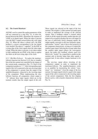
Fig. 5 shows the schematic of a summer with
independent tuning of input weights. Additional
summation (without independent tuning) can be
realized by connecting several signals to each
input.Fig. 4. Basic analog building block of the cell.
Table 1. Selected functions of a single cell.
1. y ˆ k Á
€
i wixi
€
i wi
Á
€
j wjxj
€
j wj
2. y ˆ k Á
€
i wixi
€
i wi
3. y ˆ kxixj
4. y ˆ kx2
i
5. y ˆ k Á min…x1Y F F F Y xn†
6. y ˆ k Á max…x1Y F F F Y xn†
7. y ˆ k Á y1À6 Á
1
s ‡ a
8. y ˆ a sign…y1À7†
9. y ˆ b U…y1À7†Y U is the step function
10. y ˆ kjy1À7j
11. y ˆ xi (identity)
148 E. Pierzchala and M. Perkowski
7. A current normalizing circuit [5] is used to scale
the summer tail currents in order to implement (1); see
Fig. 6. Currents I1±I9 represent ``raw,'' i.e. unscaled,
weights. The normalizing circuit produces scaled
weight currents Iw1±Iw9, whose sum always equals Iw,
and whose ratios equal the ratios of the ``raw'' weight
currents I1±I9. Thus by programming the values of
I1±I9 the weights wi of a summer are determined
independently of the summer overall gain ks, while
programming the value of Iw determines ks. The latter
can be programmed in the range À 40 dB ± ‡ 40 dB.
This arrangement leaves the scaling circuitry out of
the signal path of the cell. Details of the digital control
of the summer are discussed in Section 4.2.
3.2. Multiplier
The multiplier [4] is obtained from the basic circuit in
Fig. 4 by replacing the two tail current sources I‡
B and
IÀ
B with signal inputs. Instead of the second summer
output, a constant can be connected to the second
input of the multiplier. The sign of the multiplier
output is also programmed.
Fig. 6. Controlling the weights of the ®rst summer.
Fig. 5. Summer.
(FPAA) Part 1: Design 149
8. 3.3. Ampli®er/Integrator
Integration is one of the basic linear signal processing
operations, and as such it should be included in a
programmable analog device. In many FPAA applica-
tions, only some cells will perform integration,
therefore the FPAA cell should provide means for
turning integration off.
It is easy to implement an ampli®er/integrator if
some kind of electronic switches, such as MOS pass-
transistors, are available. Switches can be used to
program the unity-gain frequency (by connecting or
disconnecting a number of capacitors), or to turn the
integration on and off.
There are at least two problems with switches: (1)
they are not easy to implement in some technologies,
such as bipolar, (2) they introduce parasitic time-
constants which can severely degrade the frequency
response of the circuit.
A successful implementation of a switchless
current-mode Miller ampli®er/integrator in a bipolar
transistor-array technology has been demonstrated
[16].
The input buffer k1 (Fig. 7a) comprising transistors
Q11±Q16 (Fig. 8) is based on a current ampli®er of Fig.
4. Only one of the buffer outputs is active at a time,
depending on which one of the bias sources IE11, IE12
is on.
In the integrating mode (Fig. 7a) sources IE12, IC15
and IC16 are off. The ®rst output of the buffer which is
connected to the simpli®ed gm cell (Darlington pairs
Fig. 8. Simpli®ed schematic of the ampli®er/integrator.
Fig. 7. Current-mode ampli®er/integrator: (a) integrator, (b)
ampli®er.
150 E. Pierzchala and M. Perkowski
9. Q25±Q26, Q27±Q28 and to the capacitors C ) is active.
A two-stage current ampli®er k2 (Q21±Q24, Q31±Q32,
Q35±Q36) follows gm. Q35, Q36 with active loads and
emitter follower Q37, Q38 provide voltage output.
With IE31 off, differential output current is IC33, IC34
minus collector currents of Q37, Q38. With capacitors
C this is a classic Miller integrator in differential
form, with an additional current output. The gain
(unity-gain frequency) can be changed by changing
the bias of the input buffer.
In the amplifying mode (Fig. 7b), IE11 is off, the gm
cell receives no signal, and IE32, IE33 are off. Buffer k1
feeds its output current directly to the ampli®er k2
(from collectors of Q15, Q16). The gain of this cascade
can be turned up to 60 dB by changing the bias [3,5].
Differential output current is IC33, IC34 minus collector
currents of Q33, Q34.
Figs. 9 and 10 demonstrate the frequency response
in the integrating and amplifying modes, respectively.
Adjustment of IE33 allows ®ne tuning of the phase
response in the vicinity of À 90
.
Two common-mode feedback circuits (not shown),
assure proper voltage levels at the input of the gm cell,
and the collectors of Q35 and Q36. Voltage at the
emitters of Q21 and Q22, proportional to the common-
mode voltage at the gm input, is compared to a
reference level. Correction signals are sent to the bias
sources IE11, IC13, IC14. A similar scheme is used for
Q35 and Q36.
Changing voltage gain within the integrator results
in shifting the useful range of frequencies along the
frequency axis.
3.4. Clipping Circuits
Each of the clipping blocks shown in Fig. 2 is realized
as a circuit of Fig. 4. Additional current sources are
connected on the input and the output to enable
shifting of the DC transfer characteristic as required.
With two blocks one can achieve many nonlinear
characteristics, some of them shown in Fig. 3. ki, zi, ai,
bi are the slope, zero, lower saturation level and upper
saturation level, respectively (see Fig. 3b).
4. Digital Programming and Control
The characteristics of a particular circuit implemented
in the FPAA are determined by the control circuitry,
which in general has a twofold purpose:
Fig. 9. Integrating mode frequency response.
(FPAA) Part 1: Design 151
10. 1. setting up required functions and parameters of
each cell, and
2. realizing the active-control functions of the cell
(see Section 2.4.2).
In [15] a general control scheme for these purposes
has been proposed.
A modi®ed control scheme, suitable for imple-
mentation in a high-density bipolar technology,3
is
presented in this paper. Programming an FPAA
requires setting up a number of (i) analog parameters
and (ii) binary values, such as the signs of the analog
parameters, and the enable bits.
4.1. Parametric Programming
The lack of EEPROM cells and MOS devices in
bipolar technologies makes it dif®cult to design an
analog memory cell. A simple analog memory cell
and a current source, using JFET devices (available in
some bipolar technologies) has been proposed in [20].
The cell holds an analog value for about 200 ms with
less than 1% loss, using a capacitor of 0.4 pF. A
number of such cells can be connected in a ring, and
refreshed using one analog signal line and a single
clock signal, and a token passed between the cells.
Refreshing 20 such cells would require the clock
frequency on the order of 100 kHz.
In high-density bipolar processes4
it is feasible to
use a number of simple digital-to-analog converters
(DACs) for the purpose of parametric programming.
The gain of the ®rst summer (i.e. the Iw current
(Figs. 2, 6)) is controlled with 12-bit resolution. Each
weight current I1±I9 is controlled by a 4-bit word. Two
more bits: sign si and enable eni are used for each
weight wi. Thus it is possible to set the overall gain of
the cell with resolution that is higher than the ratio
of any two of the input weights.
The gain ks of the second summer is constant and
equal to 1, and its weights are controlled by 4-bit
magnitude words and sign bits. There are no enable
bits for the second summer.
The ampli®er/integrator's gain (the unity-gain
frequency) is programmed by one bit (0 dB or 20 dB).
Each of the clipping blocks parameters is pro-
grammed by 3-bit words.
Fig. 10. Amplifying mode frequency response.
152 E. Pierzchala and M. Perkowski
11. 4.2. The Control Hardware
All DACs used to control the analog parameters of the
cell are connected in a ring (Fig. 11). A token bit,
passed between the DACs, determines the response of
a DAC to its digital inputs. When the token is present
(on), the DAC's output current follows the value input
(Fig. 12). When the token is absent (off ), the DAC
produces a current corresponding to the last digital
value latched. The token is ``captured'' by the DACon
a rising edge of the clock signal when the token input
is high. When the token is present, it sets token output
to high, enabling the next DAC in the chain to capture
the token on the next rising edge of the clock.
4.2.1. Min/Max-Follower. To realize the min/max-
follower function (see Section 2.4.2), the eni (enable)
bits of the ®rst summer are controlled by the outputs of
the current-mode comparators (Fig. 13). Each of the
comparators produces a ``1'' if the corresponding input
signal of the cell (connected to the non-inverting input
of the comparator) is greater than the output of the
ampli®er/integrator, connected to the inverting input
of the comparator. When implementing the min-
follower function, all comparators whose output is
``0'' indicate these input signals which are at the
moment smaller than the output signal of the cell.
These signals are selected on the input of the ®rst
summer. The weights wi of this summer are made equal
in order to implement the average of the selected
signals. Thus a feedback scheme is formed which
results in all the signals presently smaller than the cell
output to be averaged to produce the new cell output. In
the case of suf®ciently slowly changing signals, the
output rapidly converges to the true minimum signal,
and remains ``locked'' onto it due to the hysteresis in
the comparator characteristic, so long as it is indeed the
smallest input signal. Selecting the average rather than
the smallest input signal reduces the convergence
speed, but makes this feedback scheme much less
likely to be ``fooled'' by a signal that is smallest at the
moment only to become larger than other signals a
moment later. It also allows simpler hardware to be
used.
The minamax signal allows inverting of the
comparators outputs in order to implement the
maximum-follower. The ampli®er/integrator works
as an ampli®er by transmitting the current ``max-
imum'' (or ``minimum'') from the output of the ®rst
summer. Its output signal (which is equal to the output
signal of the cell) is connected to the inverting inputs
of the current comparators. Only the ®rst clipping
block is active, with a transfer characteristic shown in
Fig. 3a.
Fig. 11. A ring of DACs.
Fig. 12. Token timing diagram.
(FPAA) Part 1: Design 153
12. Fig. 14 shows results of functional simulation of
the maximum-follower.
4.2.2. VCO. In the VCO mode, only one com-
parator in the control block is enabled. The disabled
comparators produce a ``0'' on their outputs. The
active comparator's non-inverting input receives a
constant signal from the input of the cell. The
inverting input receives the output of the integrator,
which ramps up or down at the rate determined by the
sum of other input signals of the cell. When the output
of the integrator achieves the level of the input
Fig. 13. The control circuitry of the cell.
Fig. 14. Maximum-follower operation.
154 E. Pierzchala and M. Perkowski
13. threshold signal, the comparator produces (Fig. 13)
``1'' which propagates through the 9-input OR gate to
the analog signal inverter and to the sign bit of the
multiplier. Inverting the input of the integrator results
in a ramp in the opposite direction. On the other hand,
since the integrator output signal passes through the
signal inverter, the comparator will again see a signal
which ramps up. The process continues to produce
waveforms shown in Fig. 15.
The VCO can be controlled by an input signal, or
digitally, by changing the relevant input summer
weights.
5. Conclusions
The design of a high-frequency, bipolar-technology-
based FPAA has been presented. Due to predomi-
nantly local signal interconnections and absence of
switches in the signal path, high-frequency perfor-
mance is sacri®ced to the smallest possible degree.
A companion paper [17] submitted to this issue
demonstrates a variety of applications of the FPAA.
These applications effectively prove that limitations
imposed on the architecture of the FPAA do not
essentially limit its ¯exibility.
Notes
1. The upper limit on the current gain of a single-stage current
ampli®er of Fig. 4 is near b of the transistors. When several
ampli®ers are cascaded, however, controlling of their gain
becomes dif®cult unless the gain is limited to about 10.
2. CPI transistor-array process, Maxim Integrated Products;
production-quality models were used for simulation.
3. Such as GST-2 from Maxim Integrated Products.
4. Such as GST-2 from Maxim; up to 200,000 transistors on a die.
References
1. D. R. D'Mello and P. G. Gulak, ``Design Approaches to Field
Programmable Analog Integrated Circuits.'' this issue.
2. EPAC, ``Electronically Programmable Analog Circuit.'' IMP,
Inc., San Jose, Calif.
3. B. Gilbert, ``A New Wide-Band Ampli®er Technique.'' IEEE J.
Solid-State Circ. SC-3(4), pp. 353±365, Dec. 1968.
4. B. Gilbert, ``A Precise Four-Quadrant Multiplier with
Subnanosecond Response.'' IEEE J. Solid-State Circ.
SC-3(4), pp. 365±373, Dec 1968.
5. B. Gilbert, ``Current-mode Circuits From a Translinear
Viewpoint: A Tutorial.'' in Analogue IC Design: the current-
mode approach, ed. C. Toumazou, F. J. Lidgey, and D. G.
Haigh, pp. 11±91, Peter Peregrinus Ltd., 1990.
6. F. Goodenough, ``Analog Counterparts of FPGAs Ease System
Design.'' Electronic Design, pp. 63±73, Oct. 14, 1994.
7. A. B. Grebene, Bipolar and MOS Analog Integrated Circuit
Design. J. Wiley, 1984.
Fig. 15. VCO operation.
(FPAA) Part 1: Design 155
14. 8. P. R. Grey and R. G. Meyer, Analysis and Design of Analog
Integrated Circuits. 3rd ed., J. Wiley, 1993.
9. A. Hausner, Analog and Analog/Hybrid Computer
Programming. Prentice-Hall, Inc., Englewood Cliffs, N.J.,
1971.
10. E. K. F. Lee and P. G. Gulak, ``A CMOS Field-Programmable
Analog Array.'' IEEE ISSCC Dig. Technical Papers, San
Francisco, Calif., Feb. 1991.
11. E. K. F. Lee and P. G. Gulak, ``A CMOS Field-Programmable
Analog Array.'' IEEE J. Solid-State Circ. 26(12), pp. 1860±
1867, Dec. 1991.
12. E. K. F. Lee and P. G. Gulak, ``Field Programmable Analogue
Array Based on MOSFET Transconductors.'' IEE Electronics
Letters 28(1), pp. 28±29, IEE, Jan. 2 1992.
13. E. K. F. Lee and P. G. Gulak, ``MOS Transconductor-Based
Field-Programmable Analog Array.'' IEEE ISSCC Dig.
Technical Papers, San Francisco, Calif., Feb. 1995.
14. E. Pierzchala and M. A. Perkowski, ``High Speed Field
Programmable Analog Array Architecture Design.'' Proc.
FPGA Workshop, Berkeley, California, Feb 1994.
15. E. Pierzchala and M. A. Perkowski, ``A Field-Programmable
Analog Array for Continuous, Fuzzy, and Multi-Valued Logic
Applications.'' Proc. IEEE ISMVL, Boston, Mass., May 1994.
16. E. Pierzchala, M. A. Perkowski, P. Van Halen, and R.
Schaumann, ``Current-Mode Ampli®er/Integrator for a Field-
Programmable Analog Array.'' IEEE ISSCC Dig. Technical
Papers, San Francisco, Calif., Feb. 1995.
17. E. Pierzchala and M. A. Perkowski, ``A High-Frequency Field-
Programmable Analog Array (FPAA)ÐPart 2: Applications.''
this issue.
18. R. Schaumann, M. S. Ghausi, and K. R. Laker, Design of
Analog Filters. Prentice Hall, Englewood Cliffs, NJ, 1990.
19. R. Schaumann, personal communication.
20. O. K. Shana'a, ``Circuit Implementation of a High-Speed
Continuous-Time Current-Mode Field Programmable Analog
Array (FPAA).'' MSc thesis, Portland State Univ., 1996.
21. Martin W. Snelgrove, Panel Discussion ``On the Future of
Analog Circuits'', IEEE ISCAS'96, Atlanta, Georgia, May
1996.
22. M. A. Tan, ``Design and Automatic Tuning of Fully Integrated,
Transconductance-Grounded Capacitor Filters.'' Ph.D. Thesis,
Univ. of Minnesota, 1988.
Marek A. Perkowski received his M.S. and
Ph.D. degrees from Warsaw University of
Technology, Warsaw, Poland. He studied pure
mathematics at the University of Warsaw and arti®cial
intelligence in Polish Academy of Sciences. He has
been on the faculty at the Institute of Automatic
Control, Warsaw University of Technology;
Department of Electrical Engineering, University of
Minnesota; and is currently a Professor at the
Department of Electrical Engineering, Portland State
University. His interests are in design automation,
logic synthesis, machine learning and digital and
analog ®eld-programmable gate arrays. He spent the
summer of 1994 in Wright Laboratories, Wright-
Patterson Air Force Base, working on application of
boolean decomposition to machine learning and was a
Visiting Professor at the university of Montpellier and
Technical University of Eindhoven in 1996.
He has consulted for several companies in these
areas, and also worked for Cypress Semiconductor
Corp. as a programmer and system designer of WARP,
the ®rst VHDL compiler for EPLDs.
Edmund Pierzchala received his M.S. degree in
electronic engineering from Warsaw University of
Technology, Warsaw, Poland. He worked as a research
assistant and a senior research assistant in the Institute
of Biocybernetics and Biomedical Engineering of
Polish Academy of Sciences in Warsaw, Poland, and
the Nuclear Research Institute in Swierk, Poland. He
is presently completing his Ph.D. degree at the
Department of Electrical Engineering of Portland
State University, where he also taught a number of
undergraduate and graduate courses in EE. His
research interests include programmable analog
circuits, design automation, analog and mixed-signal
circuits design, modeling, and simulation.
156 E. Pierzchala and M. Perkowski