This document describes the design of a low frequency filter using an operational transconductance amplifier (OTA). It begins with an introduction explaining that biomedical signals are usually low frequency (10 mHz to 500 Hz) and require low power and portable equipment. OTA filters can meet these needs. It then discusses OTA circuit design principles and how to simulate a resistor using an OTA. The document presents circuits for simulating a positive floating resistor with one or two OTAs. It describes using these OTA resistor simulations to design an OTA-C low pass filter and shows simulation results validating the theoretical cut-off frequencies achieved by varying the bias current.
This paper presents the design of folded cascode operational transconductance amplifier (OTA). This
design has been implemented in 0.18um CMOS Technology using Cadence. Spectre simulation shows
that the OTA has flat gain of 47dB from 1Hz to 100 KHz frequency, indicating stability of OTA, noise
ranges as 22.49769nV/ at 10Hz to 66.89128fV/ at 1MHz and average power as 0.770mW. In
this paper, we will be studying the design concepts, analysis of operational transconductance amplifier
which is used for recording the bio signals. This paper plays a key role in real time applications for
equipment designing of ECG, EEG, EMG, ENG devices. It is also used in recording and also for
treatment of Paralysis, Epilepsy, Neuro diseases etc.,
Hardware Analysis of Resonant Frequency Converter Using Isolated Circuits And...IJERD Editor
-LLC resonant frequency converter is basically a combo of series as well as parallel resonant ckt. For
LCC resonant converter it is associated with a disadvantage that, though it has two resonant frequencies, the
lower resonant frequency is in ZCS region[5]. For this application, we are not able to design the converter
working at this resonant frequency. LLC resonant converter existed for a very long time but because of
unknown characteristic of this converter it was used as a series resonant converter with basically a passive
(resistive) load. . Here, it was designed to operate in switching frequency higher than resonant frequency of the
series resonant tank of Lr and Cr converter acts very similar to Series Resonant Converter. The benefit of LLC
resonant converter is narrow switching frequency range with light load[6] . Basically, the control ckt plays a
very imp. role and hence 555 Timer used here provides a perfect square wave as the control ckt provides no
slew rate which makes the square wave really strong and impenetrable. The dead band circuit provides the
exclusive dead band in micro seconds so as to avoid the simultaneous firing of two pairs of IGBT’s where one
pair switches off and the other on for a slightest period of time. Hence, the isolator ckt here is associated with
each and every ckt used because it acts as a driver and an isolation to each of the IGBT is provided with one
exclusive transformer supply[3]. The IGBT’s are fired using the appropriate signal using the previous boards
and hence at last a high frequency rectifier ckt with a filtering capacitor is used to get an exact dc
waveform .The basic goal of this particular analysis is to observe the wave forms and characteristics of
converters with differently positioned passive elements in the form of tank circuits.
Design of Ota-C Filter for Biomedical ApplicationsIOSR Journals
Abstract-This paper presents design of operational transconductance amplifier is to amplify the ECG signal
having low frequency of 300Hz, with the supply voltage of 0.8v. To reduce the power dissipation of 779nW, by
using fifth order low pass filter. The OTA-C filter is to eliminate noise voltage and increases the reliability of
the system. A chip is fabricated in a 0.18μm CMOS process is simulated and measured to validate the system
performance using HSPICE.
Webinar Slides: Measurements and Analysis for Switched-mode Power Designsteledynelecroy
This webinar covers the measurements of interest for designers of switched-mode power conversion circuits and devices. With the goal of high efficient and reliable designs, we review the acquisition of voltage and current, their relationship in switched-mode power conversion circuits.
We review specific power circuit performance areas including the analysis of power device switching losses, conduction losses, dynamic on-resistance, control loop response, power quality, conducted emissions, best practices for probing power circuits, and power rail integrity measurements.
Open Loop Control Of Series Parallel Resonant ConverterIDES Editor
Resonant converters are desirable for power
conversion due to their comparatively smaller size and
lower power losses resulting from high-frequency
operation and inherent soft switching. Among all the
topologies of the resonant converters, the series–parallel
resonant converter (SPRC) is known to have the
combined merits of the series resonant converter and
parallel resonant converter. The converter can regulate
the output voltage at a constant switching frequency even
for a change in load resistance from full load resistance to
infinity while maintaining good part load efficiency. The
purpose of this project is to design a closed loop
controller for the phase-controlled series parallel
resonant converter (PC SPRC). The open loop analysis
and closed loop control has been provided in this paper.
This work presents investigation of passive filter performance on three-phase inverter with 180° conduction mode. The simulation model of the inverter is developed by using MATLAB/Simulink. The power circuit used Insulated Gate Bipolar Transistor (IGBT) as switching device. The inverter is controlled by using bipolar Sinusoidal Pulse Width Modulation (SPWM) technique. The IGBT was set to 25 kHz for switching frequency (fs). Three types of passive filters which are LC, RC and PI filters are used to investigate the ability to remove the unwanted signal that occurred on the inverter. The result is analyzed based on the performances of output filter in term of Total Harmonic Distortion in voltage (THDv), current (THDi), shape of output voltage and current. The THD must be less than 5% at rated inverter output voltage or current by referring to IEC 61727 Standard. The passive filter is modeled in MATLAB/Simulink environment to study the characteristics and performance of the filters.
Various Resonant Converters for high voltage and high power applications have been designed. Different Topologies of LLC, LCC, and CLL Resonant Converters have been simulated and compared for the same input voltage. The simulation was done at a very high frequency. The Output Power and the Efficiency of all the three Resonant Converters were calculated.With the results, it has been proved that LCC Resonant Converters were very much suited to give an output voltage of around 62 Kilovolts with a output power of 20 kilowatts.
A High-Swing OTA with wide Linearity for design of self-tunable linear resistorVLSICS Design
Low power consumption, long battery life and portability are essential requirements of modern health monitoring products. Operational Transconductance Amplifier (OTA) operating in subthreshold region is an basic building block for low power health monitoring products design. An modified design of OTA which incorporates better linearity and increased output impedance has been discussed in this paper. The proposed OTA uses High-swing improved-Wilson current mirror for low power and low-frequency applications. The achieved linearity is about ± 1.9 volt and unity gain bandwidth (UGB) of 342.30 KHz at power supply of 0.9 volt which makes OTA to consume power in range of nanowatts. The proposed low voltage OTA implementation in design of self- tunable linear resistor has been presented in this paper. The circuit implementation has been done using standard 0.18 micron technology provided by TSMC on BSIM 3v3 level-53 model parameter and verified results through use of ELDO Simulator.
Novel Voltage Mode Multifunction Filter based on Current Conveyor Transconduc...IDES Editor
This paper presents a novel voltage mode (VM) first
order Single input three output multi function filter employing
second generation current conveyor transconductance
amplifier (CCII-TA). The proposed circuit employs only one
active element, one grounded capacitor and three resistors.
The angular pole frequency of the proposed circuits can be
tuned electronically with the help of bias current. The proposed
circuit is very appropriate to further develop into an integrated
circuit. Sensitivity study is provided and SPICE simulations
have been included which verify the workability of the circuit
A complete description of including circuit diagram, gain equation, features of Instrumentational amplifier , its working principle, applications, practical circuits, Proteus simulation and conclusion.
Uet, Peshawar Pakistan
Batch-06
On Chip Calibration And Compensation Techniques (11 03 08)imranbashir
The advent of CMOS technology in RF integrated circuits has lead to integration. A practical manifestation of such SoC is DRP, a solution engineered at Texas Instruments Inc. in which digital baseband has been integrated with a RF transceiver all in CMOS technology. A logical step forward in use of such technology is to harness the power of the digital architecture and the baseband in implementing innovative solutions to enhance radio performance over corner conditions and mitigate interferences arising as a result of integration. This research focuses on five practical examples of software solutions for common challenges in DRP.
BASK Generator using analog switch
BFSK Generator using analog switch
BPSK Generator using analog switch
MATLAB EXPERIMENTS
4.Mean square estimation of signals
5. BASK
6. BFSK
7. BPSK
MICROWAVE EXPERIMENTS
8.Klystron characteristics
9.Frequency and wavelength measurement
10.VSWR measurement
Implementation of Fully Differential OTA based on Commercially Available IC f...IDES Editor
This article presents a realization of a recently basic
building block for analog signal processing, namely fully
differential operation transconductance amplifier (FD-OTA)
using the commercially available ICs (LT1228). The proposed
element has very simple internal instruction. The
performances are examined through PSpice simulations. The
description include example as biquadratic filter topology.
They show good agreement as theoretically depicted.
Design and analysis of operational transconductance amplifier using pspiceeSAT Publishing House
IJRET : International Journal of Research in Engineering and Technology is an international peer reviewed, online journal published by eSAT Publishing House for the enhancement of research in various disciplines of Engineering and Technology. The aim and scope of the journal is to provide an academic medium and an important reference for the advancement and dissemination of research results that support high-level learning, teaching and research in the fields of Engineering and Technology. We bring together Scientists, Academician, Field Engineers, Scholars and Students of related fields of Engineering and Technology
Simulated Analysis of Resonant Frequency Converter Using Different Tank Circu...IJERD Editor
LLC resonant frequency converter is basically a combo of series as well as parallel resonant ckt. For
LCC resonant converter it is associated with a disadvantage that, though it has two resonant frequencies, the
lower resonant frequency is in ZCS region [5]. For this application, we are not able to design the converter
working at this resonant frequency. LLC resonant converter existed for a very long time but because of
unknown characteristic of this converter it was used as a series resonant converter with basically a passive
(resistive) load. . Here, it was designed to operate in switching frequency higher than resonant frequency of the
series resonant tank of Lr and Cr converter acts very similar to Series Resonant Converter. The benefit of LLC
resonant converter is narrow switching frequency range with light load[6] . Basically, the control ckt plays a
very imp. role and hence 555 Timer used here provides a perfect square wave as the control ckt provides no
slew rate which makes the square wave really strong and impenetrable. The dead band circuit provides the
exclusive dead band in micro seconds so as to avoid the simultaneous firing of two pairs of IGBT’s where one
pair switches off and the other on for a slightest period of time. Hence, the isolator ckt here is associated with
each and every ckt used because it acts as a driver and an isolation to each of the IGBT is provided with one
exclusive transformer supply[3]. The IGBT’s are fired using the appropriate signal using the previous boards
and hence at last a high frequency rectifier ckt with a filtering capacitor is used to get an exact dc
waveform .The basic goal of this particular analysis is to observe the wave forms and characteristics of
converters with differently positioned passive elements in the form of tank circuits. The supported simulation
is done through PSIM 6.0 software tool
Efficient Design of Differential Trans- Conductance Amplifier with Sub-Thresh...IJEEE
In this paper, a low voltage differential CMOS trans-conductance amplifier using 180nm on cadence is presented. This design operates in sub threshold region of ±0.5V-1.5V and biasing stabilization has been checked by observing relationship between differential voltage and biasing variations on Nano-scale. Simulation results shows maximum differential output is obtained when biasing current reaches 500nA with CMRR 88db and static power consumption on normal input conditions is 241nW. In this paper, layout of OTA has been presented after verifying DRC and LVS by using assura tool of cadence suite.
Analysis of a Quasi Resonant Switch Mode Power Supply for Low Voltage Applica...IDES Editor
QRC provides efficient and regulated switch mode
power supplies for robotic and satellite applications. This paper
addresses the enhanced controller techniques for high
frequency isolation based push-pull Quasi Resonant
Converter. This technique is similar to the conventional PI
controller technique but varies only the enhancement
constants to improve the time domain response of the
converter. The proposed converter is designed for low output
voltage and power rating, characteristically 5V and 5 W, with
the comprehension of current design trends towards enhanced
performance. At the primary stage, to validate the design of
the converter, simulation is performed in PSIM for ±50% load
variations. A prototype model of this converter is developed.
The results obtained from the experimental set-up are
presented and analysed in detail. The results reveal the
superiority of the proposed method.
Development of a group of low power, low noise, operational amplifiers for Biomedical and Biotechnology instrumentation applications. Application is demonstrated to implement high performance single slope and dual slope Analog to Digital Converters (ADC). By Kevin Glass.
IJRET : International Journal of Research in Engineering and Technology is an international peer reviewed, online journal published by eSAT Publishing House for the enhancement of research in various disciplines of Engineering and Technology. The aim and scope of the journal is to provide an academic medium and an important reference for the advancement and dissemination of research results that support high-level learning, teaching and research in the fields of Engineering and Technology. We bring together Scientists, Academician, Field Engineers, Scholars and Students of related fields of Engineering and Technology
Study and implementation of comparator in cmos 50 nm technologyeSAT Journals
Abstract This paper describes the comparator circuits used in FLASH Analog to digital converter (ADC). The performance of FLASH ADC is greatly influenced by the choice of comparator. In this paper, first a single ended “Threshold Inverter Quantizer” (TIQ) is presented. The TIQ comparator is based on a CMOS inverter cell, in which voltage transfer characteristics (VTC) are changed by systematic transistor sizing. However, TIQ comparator is very sensitive to power supply noise. Another comparator circuit presented in this paper is “Two stage open loop comparator”. It is implemented in 50 nm CMOS Technology. Pre-simulation of comparator is done in LT-Spice and post layout simulation is done in Microwind 3.1. Keywords: CMOS, Comparator, TIQ (Threshold Inverter Quantizer), LT-Spice.
IJRET : International Journal of Research in Engineering and Technology is an international peer reviewed, online journal published by eSAT Publishing House for the enhancement of research in various disciplines of Engineering and Technology. The aim and scope of the journal is to provide an academic medium and an important reference for the advancement and dissemination of research results that support high-level learning, teaching and research in the fields of Engineering and Technology. We bring together Scientists, Academician, Field Engineers, Scholars and Students of related fields of Engineering and Technology.
International Journal of Engineering Research and Applications (IJERA) is an open access online peer reviewed international journal that publishes research and review articles in the fields of Computer Science, Neural Networks, Electrical Engineering, Software Engineering, Information Technology, Mechanical Engineering, Chemical Engineering, Plastic Engineering, Food Technology, Textile Engineering, Nano Technology & science, Power Electronics, Electronics & Communication Engineering, Computational mathematics, Image processing, Civil Engineering, Structural Engineering, Environmental Engineering, VLSI Testing & Low Power VLSI Design etc.
Harmonic Compensation for Non Linear Load Using PWM Based Active Filteridescitation
In this paper the elimination of the current harmon-
ics of injected by nonlinear loads is investigated. The active
power filter proposed in this study is a Single phase voltage
source inverter (VSI) connecting to the AC mains. The dspic
controller is used to control the operation of the switches of
the inverter. Active filtering is achieved through PWM in-
verter connected next to a given nonlinear load or at the point
of the common coupling (PCC). The simulation results show
that how well the filter eliminates the harmonics of the source
current.
In this paper, we present current amplifier based transimpedance amplifier (TIA) for biosensor applications. Proposed design has low-noise, high Transimpedance gain that can be used for low current measurement applications. The current amplifier based TIA is implemented in order to resolve the fabrication issues related to high value feedback resistor. In this design, the input block to TIA is a low amplitude current amplifier. The designed amplifier is implemented in 90 nm complementary metal-oxide semiconductor (CMOS) technology. The design achieves transimpedance gain of 800 kΩ with a bandwidth of 5 kHz and input referred current noise is of 0.152 pA/√𝐻𝑍 for an input of 41 nA bypassed from current amplifier with input of 200 pA.
LF Energy Webinar: Electrical Grid Modelling and Simulation Through PowSyBl -...DanBrown980551
Do you want to learn how to model and simulate an electrical network from scratch in under an hour?
Then welcome to this PowSyBl workshop, hosted by Rte, the French Transmission System Operator (TSO)!
During the webinar, you will discover the PowSyBl ecosystem as well as handle and study an electrical network through an interactive Python notebook.
PowSyBl is an open source project hosted by LF Energy, which offers a comprehensive set of features for electrical grid modelling and simulation. Among other advanced features, PowSyBl provides:
- A fully editable and extendable library for grid component modelling;
- Visualization tools to display your network;
- Grid simulation tools, such as power flows, security analyses (with or without remedial actions) and sensitivity analyses;
The framework is mostly written in Java, with a Python binding so that Python developers can access PowSyBl functionalities as well.
What you will learn during the webinar:
- For beginners: discover PowSyBl's functionalities through a quick general presentation and the notebook, without needing any expert coding skills;
- For advanced developers: master the skills to efficiently apply PowSyBl functionalities to your real-world scenarios.
Builder.ai Founder Sachin Dev Duggal's Strategic Approach to Create an Innova...Ramesh Iyer
In today's fast-changing business world, Companies that adapt and embrace new ideas often need help to keep up with the competition. However, fostering a culture of innovation takes much work. It takes vision, leadership and willingness to take risks in the right proportion. Sachin Dev Duggal, co-founder of Builder.ai, has perfected the art of this balance, creating a company culture where creativity and growth are nurtured at each stage.
Software Delivery At the Speed of AI: Inflectra Invests In AI-Powered QualityInflectra
In this insightful webinar, Inflectra explores how artificial intelligence (AI) is transforming software development and testing. Discover how AI-powered tools are revolutionizing every stage of the software development lifecycle (SDLC), from design and prototyping to testing, deployment, and monitoring.
Learn about:
• The Future of Testing: How AI is shifting testing towards verification, analysis, and higher-level skills, while reducing repetitive tasks.
• Test Automation: How AI-powered test case generation, optimization, and self-healing tests are making testing more efficient and effective.
• Visual Testing: Explore the emerging capabilities of AI in visual testing and how it's set to revolutionize UI verification.
• Inflectra's AI Solutions: See demonstrations of Inflectra's cutting-edge AI tools like the ChatGPT plugin and Azure Open AI platform, designed to streamline your testing process.
Whether you're a developer, tester, or QA professional, this webinar will give you valuable insights into how AI is shaping the future of software delivery.
Neuro-symbolic is not enough, we need neuro-*semantic*Frank van Harmelen
Neuro-symbolic (NeSy) AI is on the rise. However, simply machine learning on just any symbolic structure is not sufficient to really harvest the gains of NeSy. These will only be gained when the symbolic structures have an actual semantics. I give an operational definition of semantics as “predictable inference”.
All of this illustrated with link prediction over knowledge graphs, but the argument is general.
UiPath Test Automation using UiPath Test Suite series, part 4DianaGray10
Welcome to UiPath Test Automation using UiPath Test Suite series part 4. In this session, we will cover Test Manager overview along with SAP heatmap.
The UiPath Test Manager overview with SAP heatmap webinar offers a concise yet comprehensive exploration of the role of a Test Manager within SAP environments, coupled with the utilization of heatmaps for effective testing strategies.
Participants will gain insights into the responsibilities, challenges, and best practices associated with test management in SAP projects. Additionally, the webinar delves into the significance of heatmaps as a visual aid for identifying testing priorities, areas of risk, and resource allocation within SAP landscapes. Through this session, attendees can expect to enhance their understanding of test management principles while learning practical approaches to optimize testing processes in SAP environments using heatmap visualization techniques
What will you get from this session?
1. Insights into SAP testing best practices
2. Heatmap utilization for testing
3. Optimization of testing processes
4. Demo
Topics covered:
Execution from the test manager
Orchestrator execution result
Defect reporting
SAP heatmap example with demo
Speaker:
Deepak Rai, Automation Practice Lead, Boundaryless Group and UiPath MVP
Accelerate your Kubernetes clusters with Varnish CachingThijs Feryn
A presentation about the usage and availability of Varnish on Kubernetes. This talk explores the capabilities of Varnish caching and shows how to use the Varnish Helm chart to deploy it to Kubernetes.
This presentation was delivered at K8SUG Singapore. See https://feryn.eu/presentations/accelerate-your-kubernetes-clusters-with-varnish-caching-k8sug-singapore-28-2024 for more details.
Connector Corner: Automate dynamic content and events by pushing a buttonDianaGray10
Here is something new! In our next Connector Corner webinar, we will demonstrate how you can use a single workflow to:
Create a campaign using Mailchimp with merge tags/fields
Send an interactive Slack channel message (using buttons)
Have the message received by managers and peers along with a test email for review
But there’s more:
In a second workflow supporting the same use case, you’ll see:
Your campaign sent to target colleagues for approval
If the “Approve” button is clicked, a Jira/Zendesk ticket is created for the marketing design team
But—if the “Reject” button is pushed, colleagues will be alerted via Slack message
Join us to learn more about this new, human-in-the-loop capability, brought to you by Integration Service connectors.
And...
Speakers:
Akshay Agnihotri, Product Manager
Charlie Greenberg, Host
Essentials of Automations: Optimizing FME Workflows with ParametersSafe Software
Are you looking to streamline your workflows and boost your projects’ efficiency? Do you find yourself searching for ways to add flexibility and control over your FME workflows? If so, you’re in the right place.
Join us for an insightful dive into the world of FME parameters, a critical element in optimizing workflow efficiency. This webinar marks the beginning of our three-part “Essentials of Automation” series. This first webinar is designed to equip you with the knowledge and skills to utilize parameters effectively: enhancing the flexibility, maintainability, and user control of your FME projects.
Here’s what you’ll gain:
- Essentials of FME Parameters: Understand the pivotal role of parameters, including Reader/Writer, Transformer, User, and FME Flow categories. Discover how they are the key to unlocking automation and optimization within your workflows.
- Practical Applications in FME Form: Delve into key user parameter types including choice, connections, and file URLs. Allow users to control how a workflow runs, making your workflows more reusable. Learn to import values and deliver the best user experience for your workflows while enhancing accuracy.
- Optimization Strategies in FME Flow: Explore the creation and strategic deployment of parameters in FME Flow, including the use of deployment and geometry parameters, to maximize workflow efficiency.
- Pro Tips for Success: Gain insights on parameterizing connections and leveraging new features like Conditional Visibility for clarity and simplicity.
We’ll wrap up with a glimpse into future webinars, followed by a Q&A session to address your specific questions surrounding this topic.
Don’t miss this opportunity to elevate your FME expertise and drive your projects to new heights of efficiency.
JMeter webinar - integration with InfluxDB and GrafanaRTTS
Watch this recorded webinar about real-time monitoring of application performance. See how to integrate Apache JMeter, the open-source leader in performance testing, with InfluxDB, the open-source time-series database, and Grafana, the open-source analytics and visualization application.
In this webinar, we will review the benefits of leveraging InfluxDB and Grafana when executing load tests and demonstrate how these tools are used to visualize performance metrics.
Length: 30 minutes
Session Overview
-------------------------------------------
During this webinar, we will cover the following topics while demonstrating the integrations of JMeter, InfluxDB and Grafana:
- What out-of-the-box solutions are available for real-time monitoring JMeter tests?
- What are the benefits of integrating InfluxDB and Grafana into the load testing stack?
- Which features are provided by Grafana?
- Demonstration of InfluxDB and Grafana using a practice web application
To view the webinar recording, go to:
https://www.rttsweb.com/jmeter-integration-webinar
State of ICS and IoT Cyber Threat Landscape Report 2024 previewPrayukth K V
The IoT and OT threat landscape report has been prepared by the Threat Research Team at Sectrio using data from Sectrio, cyber threat intelligence farming facilities spread across over 85 cities around the world. In addition, Sectrio also runs AI-based advanced threat and payload engagement facilities that serve as sinks to attract and engage sophisticated threat actors, and newer malware including new variants and latent threats that are at an earlier stage of development.
The latest edition of the OT/ICS and IoT security Threat Landscape Report 2024 also covers:
State of global ICS asset and network exposure
Sectoral targets and attacks as well as the cost of ransom
Global APT activity, AI usage, actor and tactic profiles, and implications
Rise in volumes of AI-powered cyberattacks
Major cyber events in 2024
Malware and malicious payload trends
Cyberattack types and targets
Vulnerability exploit attempts on CVEs
Attacks on counties – USA
Expansion of bot farms – how, where, and why
In-depth analysis of the cyber threat landscape across North America, South America, Europe, APAC, and the Middle East
Why are attacks on smart factories rising?
Cyber risk predictions
Axis of attacks – Europe
Systemic attacks in the Middle East
Download the full report from here:
https://sectrio.com/resources/ot-threat-landscape-reports/sectrio-releases-ot-ics-and-iot-security-threat-landscape-report-2024/
GraphRAG is All You need? LLM & Knowledge GraphGuy Korland
Guy Korland, CEO and Co-founder of FalkorDB, will review two articles on the integration of language models with knowledge graphs.
1. Unifying Large Language Models and Knowledge Graphs: A Roadmap.
https://arxiv.org/abs/2306.08302
2. Microsoft Research's GraphRAG paper and a review paper on various uses of knowledge graphs:
https://www.microsoft.com/en-us/research/blog/graphrag-unlocking-llm-discovery-on-narrative-private-data/
Monitoring Java Application Security with JDK Tools and JFR Events
D04462128
1. IOSR Journal of Engineering (IOSRJEN) www.iosrjen.org
ISSN (e): 2250-3021, ISSN (p): 2278-8719
Vol. 04, Issue 04 (April. 2014), ||V6|| PP 21-28
International organization of Scientific Research 21 | P a g e
Low Frequency Filter Design using Operational
Transconductance Amplifier
Dr Rajeshwari S Mathad
Department of Electronics, Basaveshwar Science College,BAGALKOT
Abstract: - Biomedical signal processing requires low power consumption and low frequency filters.
Biomedical signals are usually of 10-mHz to 100-Hz and maximum of 500Hz frequency range. The equipments
used in the design of biomedical applications require portability and circuit needs to be operated with low
supply voltage. These requirements can be fulfilled by using active filters designed by Operational
Transconductance Amplifier.
Keywords: Operational Transconductance Amplifier (OTA) , OTA-C, Operational Transconductance Amplifier
– Capacitor.
I. INTRODUCTION
Integrated circuit technologies for biomedical applications have been widely used in recent years. The
instruments used in biomedical applications may be having some restrictions on battery charges for all portable
electronic devices. To satisfy with ambulatory functions the circuit should not only with low power but also
with low voltage. Therefore in this paper a low power- low voltage Operational Transconductance Amplifier
(OTA) is used to design a low frequency active low pass filter, thus component count can be drastically
reduced. The circuit can be operated with low supply voltage of order 1.8V, high stability and linearity in the
response, with high signal to noise ratio can be obtained. The required cut off frequency can be tuned
electronically. All these requirements cannot be fulfilled in the filter design using operational amplifier. In
active filter design using operational amplifier, electronic tuning is not possible. To change the value of cut off
frequency calculations has to be done to change values of resistance and capacitance. Portability cannot be
obtained in active filters using operational amplifiers because the component count is more in comparison with
OTA active filters [1]-[3].
The time constant of operational transconductance amplifier-capacitor (OTA-C) filter is determine by
the ratio of load capacitor to the OTA transconductance, i.e C/gm. For an OTA-C filter implementation in low
frequency implies large capacitance and very low transconductance [4]-[5]. Thus there are two different
techniques to solve this problem. One is to design an OTA with very low transconductance and another is to
realize filter with large load capacitance. In this paper, current division technique is used to obtain a low
transconductance, for implementation of very large time constant. Using this technique an OTA-C active filter
can be designed for low frequency applications.
In this paper, a low frequency Active filter design using OTA has been explained. The total number of
components used in these circuits are very small, the design equations and voltage- current characteristics are
attractive. An improvement in design simplicity is observed in comparison with op amp based structures. An
OTA is a voltage controlled current source, more specifically the term “operational” comes from the fact that it
takes the difference of two voltages at the input, and converts it into output current.
The ideal transfer characteristic of OTA is Io = gm (V1+
- V2-
)
Where V1+
- V2-
is a differential input voltage and Io is a output current and gm is the transconductance gain of
OTA.
By taking the pre-computed difference as the input, Io = gm Vin
The transconductances gm is also a function of the input differential voltage. The term “transconductance” in
OTA is the ratio of output current to the input voltage, gm, has the unit of conductance.
2. Low Frequency Filter Design using Operational Transconductance Amplifier
International organization of Scientific Research 22 | P a g e
Figure 1. Circuit symbol of OTA
II. PRINCIPLE OF OPERATION AND CIRCUIT ANALYSIS
OTA-based filters are composed of the open-loop OTA-C integrators in which the devices are operated
in the subthreshold region to realize a very low transconductances, typically of the order of a few nano amperes.
In OTA-based circuits, the bias current will dominate the performance of the filter circuit, and the ratio of
capacitance to small transconductance determines the time constant of OTA-C integrators [4].
An active RC filter can be designed using OTA as a variable resistance simulator. Variable resistors are
one of the applications of OTA. There are two types of OTA variable resistance simulators , those are positive
resistance simulator and negative resistance simulator, depending on their feedback polarities. "Fig 2" and
“Fig 3" shows two positive resistance simulators, realized using negative feedback. The input impedance of
these two versions can be derived by assuming an input voltage vi and an input current ii for each version.
Zi = vi / ii = 1/ gm
OTA is assumed to have a transconductance gm. At frequencies much lower than the cut off frequency
of the OTAs, gm is real, thus Zi becomes a resistor using single OTA and two OTAs. Resistance values are
realized by varying the bias current of the OTA. OTA variable resistors with capacitors can compose OTA-C
filters, where these OTA variable resistors are used to tune the filter frequencies.
The performance of the proposed circuit is illustrated by Proteus Proffessional-7.5 simulations, which are in
accordance with theoretical predictions. In this paper for experimental work OTA LM13600 is used.
The transconductances gm is given by, gm = Ibias/ 2VT
Where VT: thermal voltage = 26 mV at room temperature, Ibias : bias current.
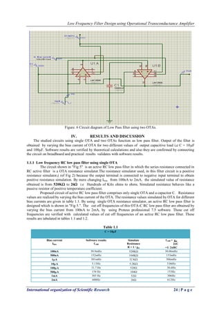
The proposed circuit of the floating positive resistance simulator is shown in "Fig. 2", where Ib is the bias current
of the OTA.
1.1 Simulation of positive floating resistance using single OTA
Consider the circuit in "Fig. 2" it is a positive resistance simulator using single OTA. By properties of the OTA,
we will get,
Req = Vin+
Vin
IR = 1/ gm
Where gm = Ibias / 2VT
Therefore , Req = 2VT / Ibias .
From above equation it is clear that resistance value can be easily electronically varied by varying the bias
current.
Figure 2 OTA simulation of floating resistor
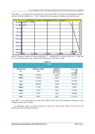
1.2 Simulation of positive floating resistance using two OTAs.
Consider the circuit shown in "Fig. 3", it is a positive resistance simulator using two OTAs. The bias
current applied for two OTAs is IB (refer in "Fig. 6"). This externally applied bias current IB divides between
two OTAs. For each OTA bias current Ib = IB / 2 . Therefore the transconductance gm for two OTAs is given by,
gm = gm . The current division concept used in this circuit is mainly useful to obtain lower value of
3. Low Frequency Filter Design using Operational Transconductance Amplifier
International organization of Scientific Research 23 | P a g e
transconductances, which helps in the design of active filters in low frequency range to obtain larger value of
time constant. The simulated resistance which depends on bias current is reciprocal transconductances gm .
Figure 3 Simulation of floating resistor using two OTAs
1.3 Low frequency RC low pass filter using OTA
A low frequency RC low pass filter is designed using OTA resistance simulator. Both type of
resistance simulators are used in filter design, i,e using single OTA and using two OTAs. “Fig 4” shows the
conventional circuit of RC low pass filter. “Fig 5” is a RC low pass filter using single OTA and “Fig 6” is a RC
low pass filter using two OTAs. Output of the filter is measured by varying the bias current to obtain required
cut off frequency.[1]-[6]
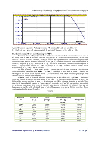
Figure 4 Conventional circuit of RC low pass filter.
III. EXPERIMENTAL SETUP
The stated circuits of “Fig 5” and “Fig 6” are simulated using Proteus professional 7.5 software. Same
circuits are arranged on bread board using an OTA LM13600 to verify the software results. Output of the filter
is observed by varying the bias current of OTAs.
Figure. 5 Circuit diagram of OTA- C Low Pass filter using software
4. Low Frequency Filter Design using Operational Transconductance Amplifier
International organization of Scientific Research 24 | P a g e
Figure. 6 Circuit diagram of Low Pass filter using two OTAs.
IV. RESULTS AND DISCUSSION
The studied circuits using single OTA and two OTAs function as low pass filter. Output of the filter is
obtained by varying the bias current of OTA for two different values of output capacitive load i,e C = 10F
and 100F. Software results are verified by theoretical calculations and also they are confirmed by connecting
the circuit on breadboard and practical results validates with software results.
1.1.1 Low frequency RC low pass filter using single OTA
The circuit shown in "Fig 5" is an active RC low pass filter in which the series resistance connected in
RC active filter is a OTA resistance simulator.The resistance simulator used, in this filter circuit is a positive
resistance simulator,( ref Fig 2) because the output terminal is connected to negative input terminal to obtain
positive resistance simulation. By mere changing Ibias from 100nA to 2mA, the simulated value of resistance
obtained is from 520K to 26 i.e Hundreds of Kilo ohms to ohms. Simulated resistance behaves like a
passive resistor of positive temperature coefficient.
Proposed circuit of active RC low pass filter comprises only single OTA and a capacitor C. Resistance
values are realized by varying the bias current of the OTA. The resistance values simulated by OTA for different
bias currents are given in table 1.1. By using single OTA resistance simulator, an active RC low pass filter is
designed which is shown in "Fig 5.". The cut off frequencies of this OTA-C RC low pass filter are obtained by
varying the bias current from 100nA to 2mA, by using Proteus professional 7.5 software. These cut off
frequencies are verified with calculated values of cut off frequencies of an active RC low pass filter. These
results are tabulated in tables 1.1 and 1.2.
Table 1.1
C = 10F
Bias current
Ibias
Software results
f-3dB
Simulate
Resistance
R = 1 / gm
f-3dB = gm
2C
=1/ 2RC
100nA 30.9mHz 520K 30.06mHz
500nA 152mHz 104K 153mHz
1A 301mHz 52 K 306mHz
10A 3.13Hz 5.2K 3.06Hz
100A 31.7 Hz 520 30.6Hz
500A 154 Hz 104 153Hz
1mA 303 Hz 52 306Hz
2mA 600Hz 26 612Hz
5. Low Frequency Filter Design using Operational Transconductance Amplifier
International organization of Scientific Research 25 | P a g e
From table 1.1 it is clear that, by varying the bias current from 100nA to 2mA the cut off frequencies obtained
are from 30.9mHz to 600Hz, for C = 10F. Theoretical cut off frequencies validates with software results.
Figure.7 Frequency response of Proteus professional 7.5 simulated OTA-C low pass filter, for C = 10F with
Ibias= 1A, with maximum. gain 0 dB and cut off frequency of 301mHz at - 3dB.
Table 1.2
C = 100F
Bias current
Ibias
Software results
f-3dB
Simulate
Resistance
R = 1 / gm
f-3dB = gm
2C
=1/ 2RC
100nA 3.09mHz 520K 3.06mHz
500nA 15.3mHz 104K 15.3mHz
1A 30.1mHz 52 K 30.6mHz
10A 209mHz 5.2K 306mHz
100A 3.13Hz 520 3.06Hz
500A 15.2Hz 104 15.30Hz
1mA 30Hz 52 30.60Hz
2mA 60Hz 26 61.21Hz
From table 1.2 by varying the bias current from 100nA to 2mA the cut off frequencies obtained are from
3.09mHz to 60Hz, for C = 100F.
As capacitance value C is further increased, for given bias currents from 100nA to 2mA the cut off
frequencies can be still further decreased.
6. Low Frequency Filter Design using Operational Transconductance Amplifier
International organization of Scientific Research 26 | P a g e
Figure.8 Frequency response of Proteus professional 7.5 simulated OTA-C low pass filter , for
C= 100F with Ibias= 1A, with maximum gain 0 dB and cut off frequency of 30.1 mHz at - 3dB.
1.1.2 Low frequency RC low pass filter using two OTAs.
The circuit shown in Figure 6 is an active RC low pass filter in which the series resistance connected in
RC active filter is a OTA resistance simulator using two OTAs.The resistance simulator used, in this filter
circuit is a positive resistance simulator,( ref Fig 3) because the output terminal is connected to negative input
terminal to obtain positive resistance simulation. In this type of resistance simulation the transconductance of
two OTAs are given by gm = gm, therefore R = 1/ gm. In case of bias current, current division takes place. It
means Ibias equally divides between two OTAs. For example if IB = 100A then bias current of each OTA will
be 50A,and gm = Ibias/ 2VT = 50A / 226mV.
By mere changing Ibias from 100nA to 4mA, it means 50nA to 2mA for each OTA , the simulated
value of resistance obtained is from 1040K to 26 i.e Thousands of Kilo ohms to ohms . Therefore the
advantage of this circuit is that, we can obtain 1 G of resistance. Such a high resistance gives larger time
constant, which is useful in filter designing. .
Proposed circuit of active RC low pass filter comprises of two OTAs and a capacitor C. Resistance
values are realized by varying the bias current of the OTA. The resistance values simulated by OTAs for
different bias currents are given in table 1.3. By using this, two OTAs resistance simulator an active RC low
pass filter is designed which is shown in Figure 6. Cut off frequencies of OTA-C RC low pass filter are obtained
by varying the bias current from 100nA to 4mA, by using Proteus professional 7.5 software. These cut off
frequencies are verified with calculated value of cut off frequencies of an active RC low pass filter. These
results are tabulated in tables 1.3 and 1.4.
Table 1.3
C = 10F
Bias current
IB
For each OTA
Ib1= Ib2
= IB/2
Simulate
Resistance
R = 1 / gm
Calculated cut off frequency
f-3dB = gm
2C
= 1/ 2RC
Software results
f-3dB
100nA 50nA 1040K 15.2mHz 15.8mHz
500nA 250nA 208K 7.63mHz 7.83mHz
1A 500nA 104K 15.2mHz 158mHz
10A 5A 10.04K 1.52Hz 1.58Hz
100A 50A 1K 15.3Hz 15.7Hz
500A 250A 208 76.4Hz 77 Hz
1mA 500A 104 152.9Hz 152 Hz
2mA 1mA 52 306 Hz 299 Hz
3mA 1.5mA 34.7 458 Hz 450 Hz
4mA 2mA 26 612Hz 600Hz
7. Low Frequency Filter Design using Operational Transconductance Amplifier
International organization of Scientific Research 27 | P a g e
Figure.9 Frequency response of Proteus professional 7.5 simulated OTA-C low pass filter circuit, for C= 10F
with Ibias= 100nA, with maximum gain 0 dB and cut off frequency of 15.2 mHz at - 3dB.
From table 1.3 it is clear that, by varying the bias current from 100nA to 4mA ,( but for each OTA bias current
IB is taken as Ib1= Ib2= IB / 2 , therefore variation of bias current is considered to be from 50nA to 2mA ) the cut
off frequencies obtained are from 15.2mHz to 612Hz, for C = 10F.
Table 1.4
C = 100 F
Bias current
Ib
For each OTA
Ib1= Ib2
= Ib/2
Simulate
Resistance
R = 1 / gm
Calculated cut off frequency
f-3dB = gm
2C
= 1/ 2RC
Software
results
f-3dB
100nA 50nA 1040K 1.52mHz 1.57mHz
500nA 250nA 208K 7.63mHz 7.86mHz
1A 500nA 104K 15.2mHz 15.6mHz
10A 5A 10.04K 152mHz 158mHz
100A 50A 1K 1.53Hz 1.57Hz
500A 250A 208 7.63Hz 7.68 Hz
1mA 500A 104 15.3Hz 15.2Hz
2mA 1mA 52 30.6Hz 29.3Hz
3m 1.5mA 34.7 45Hz 42.4Hz
4m 2mA 26 60Hz 60 Hz
.
8. Low Frequency Filter Design using Operational Transconductance Amplifier
International organization of Scientific Research 28 | P a g e
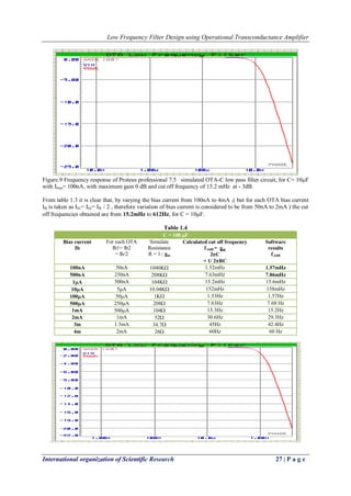
Figure.10 Frequency response of Proteus professional 7.5 simulated OTA-C low pass filter circuit, for C=
100F with Ibias= 100nA, with maximum gain 0 dB and cut off frequency of 1.52 mHz at - 3dB
From table 1.4 it is clear that by varying the bias current from 100nA to 4mA that is for each OTA it is from
50nA to 2mA the cut off frequencies obtained are from 1.52mHz to 60 Hz, for C = 100F.
As capacitance value C is further increased, for given bias currents from 50nA to 2mA , still lower
value of cut off frequencies can be obtained. Current division technique used in two OTAs filter structure to
obtain lower values of bias current implies very low transconductances. In this paper a low transconductance of
order 2siemens for the external bias 100nA for single OTA filter structure and 1siemen of transconductance
for the external bias current of 50nA for two OTAs filter structure are obtained.
V. CONCLUSION
OTA-C filter realized with minimum number of OTA’s and capacitor is an innovative method of
designing low frequency active filters which have flexibility in respect of pass band width. The above
discussion concludes that we can achieve a tunable range of low frequencies only by changing externally
accessible bias current which changes parameter gm transconductance of a device. All the requirements such as
low supply voltage of order 1.8V, low component count and portability are achieved.
OTA-C RC filters design using single OTA and two OTAs explain the application of OTA in active
filter design of low frequency of order of 3.09mHz and 1.52mHz respectively. In these low frequency filters
OTA behaves as positive resistance simulator. There is a good agreement between theoretical, and software
results and also with the experimental observations. Butterworth characteristics of filter is desirable at such low
frequency with out mixing of any noise signals[7]. The filter characteristics are stable at low frequency of
1.52mHz on wards, and have applications in, biomedical science , sensor circuits and neural networks[8].
VI. ACKNOWLEDGEMENTS
The author acknowledge the help rendered by VGST by giving level 2 assistance for the precurement of
softwares , deviceses and instruments which have been used.
REFERENCES
[1] Shuenn Yuh Lee, Chih-Jen Cheng,”Systematic Design and Modeling of a OTA-C Filter for Portable
ECG Detection” IEEE TRANSACTIONS ON BIOMEDICAL CIRCUITS AND SYSTEMS, VOL. 3, NO.
1, FEBRUARY 2009
[2] Moein Shayegannia ,Hasan Al-Nashash “Low Frequency Filter design Using Gyrator for
Biomedical Applications” American University of Sharjah, Sharjah, UAE 00017488@aus.edu and
hnashash@aus.edu
[3] Mrs. Ashu Soni, Mr. Sumit Kumar, Ms. Shivani Gupta “OTA Model Used in Active-Passive Filter for
Lowering Power Consumption” http: / www.ijesrt.com(C)International Journal of Engineering Sciences
& Research Technology
[4] G. Düzenli, Y. Kılıç, H. Kuntman and A. Ataman: “On the design of low-frequency filters using CMO
OTAs operating in the subthreshold region” Microelectronics Journal, Vol.30, No. 1, pp.45-54, 1999.
[5] Abhay Pratap Singh, Sunil Kr. Pandey, Manish Kumar “Operational Transconductance Amplifier for
Low Frequency Application ” IJCTA | MAY-JUNE 2012
[6] Siva V. Thyagarajan, , Shanthi Pavan , and Prabu Sankar “Active-RC Filters Using the Gm-Assisted
OTA-RC Technique” IEEE JOURNAL OF SOLID-STATE CIRCUITS, VOL. 46, NO. 7, JULY 2011
[7] “A Basic Introduction to Filters Active, Passive, and Switched-Capacitor ” National Semiconductor
Application Note 779 Kerry Lacanette April 1991
[8] Garima1, Priya Banga, Akshita Singh “Active Filter Design Using OTA Realization” www.ijetae.com
(ISSN 2250-2459 (Online), Volume 4, Special Issue 1, February 2014)