Download to read offline
![IOSR Journal of Electrical and Electronics Engineering (IOSR-JEEE)
e-ISSN: 2278-1676,p-ISSN: 2320-3331, Volume 10, Issue 2 Ver. III (Mar – Apr. 2015), PP 53-58
www.iosrjournals.org
DOI: 10.9790/1676-10235358 www.iosrjournals.org 53 | Page
CMOS RF Bandpass Filter Design using a Compensated Active
Inductor
1
W. El hamdani, M.El bekkali, 2
M.ALAMI, 3
F. Temcamani, B.Delacressonnière
1
Faculty of Science and Technology LTTI-Lab/ USMBA Fez, Morocco
2
CSE-Lab/ INPT Rabat, Morocco
3
ECS-Lab/ENSEA Cergy-Pontoise Cedex, France
Abstract: A novel tuning technique which improves the performances of an RF CMOS band-pass filter based
on simulated inductors is presented. Gain enhancement techniques are applied to reduce the inductor losses by
using a novel negative resistance topology. The proposed method is sufficiently general to be applied to other
active filters topologies based on active inductors as well and is intended to be used for CMOS multi-standard
filters design.
Keywords: MOS simulated inductors, active RF multi-standard filters, frequency and Q-factor tuning, negative
resistance.
I. Introduction
The growing market of wireless communications is a significant reason that motivates the study of new
low-cost and highly integrated architectures.
Radio frequency (RF) filters are essential components of any RF wireless transceiver and are used to
attenuate undesired out of band signals. RF filters typically use passive inductors; however, on-chip passive
inductors are notorious for their low quality factor and the large amount of chip area they consume [1], [2]. As a
result, RF filters are usually implemented off-chip, a process which adds extra cost and manufacturing time to the
design cycle. Indeed, spiral inductors are a critical issue in RF-design, their large on-chip area and weak quality
factor being the main constraints for highly integrated products.
Active inductors drastically reduce the required chip area while improving the quality factor and
potentially performance of the emulated inductor. Additionally, both the frequency and selectivity (bandwidth) of
the active filter can be tuned by simply changing the amount of current channeled by the transistors. This tunable
nature makes active filters especially suitable for multi-standard systems.
There are numerous topologies proposed and analyzed in literature for active inductors in CMOS
technology in a frequency range up to a few GHz [3-4]. A reference paper for simulated inductors is [3] where a
model for microwave applications is proposed.
This paper describes an architecture for a tunable active bandpass filter using the gyrator principle to
transform a capacitive impedance into an inductive one. Q-Enhancement is accomplished by using a negative
resistance coupled to active inductor. The technique presented here has a greater effect on the available tuning
range. The theory behind the filter and tuning enhancements will be described first, followed by simulation results
demonstrating the performance improvements.
II. Active inductor topology
Inductor is now becoming a highly attractive choice for CMOS wireless communication systems. Its
interesting and unique advantages over spiral inductors include the following factors:
Occupying smaller die area,
High quality factor,
Tunable inductance,
And the possibility of achieving higher inductance with high resonance frequency.
Applications of the active inductor include Wilkinson power divider [5], phase shifter [6], filter [7], [8],
oscillator [8], and current-mode phase-locked loop [9].
The concept of an active inductor is based on a well-known gyrator theory [10]. It is a two-port network
that can be realized by connecting two transconductors in negative feedback, Fig.1. Gm1 and Gm2 are the
transconductances of transconductors 1 and 2, respectively, and C is the load capacitance at node 1. The
transconductor in the forward path has a positive transconductance while the transconductor in the feedback path
has a negative transconductance.
The input admittance looking into port 2 of the gyrator-C network is given by:](https://image.slidesharecdn.com/h010235358-160705061828/85/H010235358-1-320.jpg)
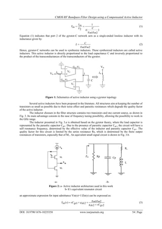
![CMOS RF Bandpass Filter Design using a Compensated Active Inductor
DOI: 10.9790/1676-10235358 www.iosrjournals.org 55 | Page
As expected, the input admittance shows that it is equivalent to an RLC network, as shown in Fig. 3.b.
The element values can be determined as follows.
21
2
mgmg
gsC
L (4)
21
1
mgmg
dsg
sR (5)
2
1
dsg
pR (6)
1gsCpC (7)
In most cases, due to the presence of the parasitic capacitor Cgs1, the active inductor is seen as a
bandpass filter with its resonant frequency.
Neglecting the transistor output resistance, the relations for the resonant frequency and quality factor are given
respectively by:
21
21
211
0 tt
gsCgsC
mgmg
pLC
(8)
2
1
21
12
/ t
t
gsCmg
gsCmg
pCL
pR
Q
(9)
Where ωt1 and ωt2 are the transit (unity-gain) frequencies of M1 and M2 respectively. Thus, for a high-
frequency active filter, both transistors need to be biased for a high unity-gain frequency. However, if M1 has a
high unity-gain frequency, (9) shows that this will also degrade the selectivity of the filter.
This problem can be circumvented by using a negative resistance circuit to compensate loss in
inductance and increase the Q of the filter.
In the following we discuss topologies of negative resistance.
III. The proposed negative resistance circuit
The negative resistance can be built by bipolar and FET devices. In the case of FET device, there are
two kinds of topology: the one using a passive feedback and one using an active feedback. In the case of passive
feedback, common-gate with inductance feedback and drain output as well as common source with capacitance
feedback and gate output are commonly used. Each method has its own working frequency and resistance value
[11].
In [12] the negative resistance circuit is using an active feedback. Among three topologies studied, a
Common Drain- Common Gate (CD-CG) structure has been proposed and represented in Fig. 3 as well, proving
to be a promising solution in compensating loss of CMOS active inductor.
Further details regarding this principle are presented in [12].
Figure 3: CD-CG negative resistance circuit
Yc
Ye
D
D](https://image.slidesharecdn.com/h010235358-160705061828/85/H010235358-3-320.jpg)
![CMOS RF Bandpass Filter Design using a Compensated Active Inductor
DOI: 10.9790/1676-10235358 www.iosrjournals.org 56 | Page
Figure 4: Small signal equivalent circuit of the negative resistance
Figure 5: Simulated resistance and reactance of the negative resistance circuit.
IV. Design of bandpass filter using compensated active inductor
A. Circuit principe
The block diagram of the RF bandpass filter based on the active inductor is shown in Fig. 6. It’s
associated in parallel with a negative conductance and a variable capacitor (varactor). This allows the adjustment
of respectively the filter bandwidth and the center frequency. It is obvious that the order of the filter can’t allow
the same response as commercial SAW filters. However we have to combine several cells coupled to have higher
levels of responses [13].
The input buffer realized by Min, converts the input voltage Vin to a current that is applied to the active
inductor [14]. This is the most effective way to change the gain of the filter. For measurement requirement, an
output buffer composed of a common-drain transistor Mout and a current source IB is added [15]. The output
buffer is used to drive the resistive loads. Besides, it prevents the load resistors and capacitors from reducing the
resonant frequency and quality factor of the filter. The output buffer provides an adequate driving current and
matching output impedance to the load. The output buffer must also have a large bandwidth so that its impact on
the performance of the filter is minimum. Source-follower configurations are typically used in realization of the
output buffer due to their low and tunable output impedance and large bandwidth.
Figure 6: Block diagram of the Bandpass filter based on compensated active inductor
B. Simulation results
This work was simulated using AMS 0.35-μm process parameters with 2.3V power supply. All
transistors have the minimum channel length of 0.35-μm. Through a S-parameter simulation the transfer function
is shown in Fig. 7. The measured centre frequency f0 is 6.2 GHz without Cv. The measured Q is 124.4.
G2
ix
gds1
~
D2G2
D1
Vx
gm1Vgs1 Cgs2
gds2
gm2Vgs2Cgs1
G1
Vin
Vout
VDD
Min
Mout
Zin Cp Rp Lp
Active inductor
IB
Output bufferInput buffer
Rn
Cv](https://image.slidesharecdn.com/h010235358-160705061828/85/H010235358-4-320.jpg)

![CMOS RF Bandpass Filter Design using a Compensated Active Inductor
DOI: 10.9790/1676-10235358 www.iosrjournals.org 58 | Page
V. Conclusions
In this paper a novel negative resistance network topology is shown to provide loss compensation on all-
transistor active inductor.
The second order bandpass filter based on this active inductor has been proposed. Q-enhancement is
accomplished by varying value of negative resistance coupled to the resonator. Tuning range of resonant
frequency is demonstrated by varying varactor Cv.
Acknowledgment
The authors would like to thank the Inter-University Joint Committee Franco-Moroccan for assistance to
this project through integrated action Volubilis. They also thank the Moroccan Ministry of Education and Higher
Education for its support through CSPT funding.
References
[1]. Y. Koutsoyannopoulos et al, ―Novel Si Integrated Inductor and Transformer Structures for RF IC Design, ‖ IEEE International
Symposium on Circuits and Systems, vol. 2, pp. 573-576, 1999.
[2]. W. B. Kuh, F. W. Stephenson, and A. Elshabini-Riad, ―A 200 MHz CMOS Q-enhanced LC Bandpass Filter, ‖ IEEE Journal of
Solid-State Circuits, vol. 31, no. 8, pp. 1112-1122, Aug. 1996.
[3]. S. Hara, T. Tokumitsu, ―Broad-Band Monolithic Microwave Active Inductor and Its Application to Miniaturized Wide-Band
Amplifiers‖, IEEE MTT, 1998, Vol. 36, No. 12.
[4]. A. Thanachayanont, ―A 1.5-V CMOS Fully Differential Inductorless RF Bandpass Amplifier‖, Proc. IEEE ISCAS, pp. 49-52, Vol.
1, 2001.
[5]. L. Liang-Hung, L. Yu-Te, and W. Chung-Ru, ―A miniaturized Wilkinson power divider with CMOS active inductors,‖ IEEE
Microw. Wireless Compon. Lett., vol. 15, no. 11, pp. 775–777, Nov. 2005.
[6]. M. A. Y. Abdalla, K. Phang, and G. V. Eleftheriades, ―Printed and integrated CMOS positive/negative refractive-index phase
shifters using tunable active inductors,‖ IEEE Trans. Microw. Theory Tech., vol. 55, no. 8, pp. 1611–1623, Aug. 2007.
[7]. Y. Wu, X. Ding, M. Ismail, and H. Olsson, ―RF bandpass filter design based on CMOS active inductors,‖ IEEE Trans. Circuits
Syst. II, vol. 50, no. 12, pp. 942–949, Dec. 2003.
[8]. A. Thanachayanont and A. Payne, ―CMOS floating active inductor and its applications to bandpass filter and oscillator designs,‖
Proc. Inst. Elect. Eng., vol. 147, pp. 42–48, Feb. 2000.
[9]. D. DiClemente and F. Yuan, ―Current-mode phase-locked loops—A new architecture,‖ IEEE Trans. Circuits Syst. II, vol. 54, no. 4,
pp. 303–307, Apr. 2007.
[10]. F. Yuan, CMOS Active Inductors and Transformers Principle, Implementation, and Applications. Springer Science + Business
Media, 2008.
[11]. U. Karacaogluand I. D. Robertson, ―MMIC active bandpass filters using varactor-tuned negative resistance elements,‖ IEEE
Transactions on Microwave Theory and Techniques, vol. 43, no. 12, pp. 2926-2932, December 1995.
[12]. W. El Hamdani, F. Temcamani, B. Delacrosonnière, M. Alami, M. El Bekkali, ―Etude de structures actives simulant une ésistance
négative intégable dans des filtres RF‖, Mediteranean Telecommunication Journal (RMT), vol. 3, n°1, P 26, Februry 2013.
[13]. Anh Dinh, Jiandong Ge, ―A Q-Enhanced 3.6 GHz, Tunable, Sixth-Order Bandpass Filter Using 0.18 μm CMOS‖, VLSI Design,
Vol 2007, Article ID 84650, 2007.
[14]. H. Xiao, R. Schaumann, and W. Daasch, ―A radio-frequency CMOS active inductor and its application in designing high-Q filters,‖
in Proc. IEEE Int’l Symp. Circuits Syst., vol. 4, Vancouver, May 2004, pp. 197–200.
[15]. Z. Gao, Y. Ye, M. Yu, and J. Ma, ―A CMOS rf tuning wide-band bandpass filter for wireless applications,‖ in Proc. IEEE Int’l
Conf. SOC., Sep 2005, pp. 79–80.](https://image.slidesharecdn.com/h010235358-160705061828/85/H010235358-6-320.jpg)

This document describes a CMOS RF bandpass filter design using an active inductor with a compensated negative resistance circuit. It begins by introducing the need for integrated RF filters and issues with passive inductors. It then describes an active inductor topology based on the gyrator principle and a common drain-common gate negative resistance circuit to compensate losses. Simulation results show the filter achieves a center frequency tuning range of 1.9-6 GHz and quality factors above 60 when tuned. The compensated active inductor approach allows for an integrated tunable bandpass filter solution for multi-standard wireless applications.