SlideShare a Scribd company logo
IOSR Journal of Electronics and Communication Engineering (IOSR-JECE)
e-ISSN: 2278-2834,p- ISSN: 2278-8735.Volume 12, Issue 2, Ver. I (Mar.-Apr. 2017), PP 52-56
www.iosrjournals.org
DOI: 10.9790/2834-1202015256 www.iosrjournals.org 52 | Page
Design of Counter Using SRAM
Rajat Kumar Dwibedi1
, L.Pattathurani2
1
(Assistant Professor/ECE, Jeppiaar SRR Engineering College, Chennai, India)
2
(Assistant Professor/EEE, Jeppiaar Institute Of Technology, Chennai, India )
Abstract: In digital logic and computing, a counter is a device which stores the number of times a particular
event or process has occurred, often in relationship to a clock signal. CMOS devices are designed for high
noise immunity and low static power consumption. CMOS accomplishes current reduction by complementing
every nMOSFET with a pMOSFET and connecting both gates and both drains together. A high voltage on
the gates will cause the nMOSFET to conduct and the pMOSFET to not conduct, while a low voltage
on the gate causes the reverse. This arrangement greatly reduces power consumption and heat generation
.Finally we proposed counter using SRAM model, provides the best resolution, high output current and good
output-input current linearity.
Keywords: CMOS(Complementary Metal Oxide Semiconductor),MOSFET(Metal Oxide Semiconductor Field
Effect Transistor), SRAM(Static Random Access Memory), TTL(Transistor Transistor Logic),VLSI(Very Large
Scale Integrated Circuits).
I. Introduction To Counter
Counter used in electronics, computing and mechanical counting devices. In digital logic a counter is a
device which stores the number of times a particular event or process has occurred, often in relationship to a
clock signal. The most common type is sequential digital logic circuit with an input line called the "clock"
and multiple output lines. The values on the output lines represent a number in the binary or BCD number
system. Each pulse applied to the clock input increments or decrements the number in the counter. A counter
circuit is usually constructed of a number of flip flops connected in cascade. Counters are a very widely-used
component in digital circuits, and are manufactured as separate integrated circuits and also incorporated as parts
of larger integrated circuits.
A. Types of Counter
There are seven types of electronic counters are as follows.
 Asynchronous (ripple) counter – changing state bits are used as clocks to subsequent state flip-flops.
 Synchronous counter – all state bits change under control of a single clock.
 Decade counter – counts through ten states per stage.
 Up/down counter – counts both up and down, under command of a control input.
 Ring counter – formed by a shift register with feedback connection in a ring.
 Johnson counter – a twisted ring counter.
 Cascaded counter.
Each is useful for different applications. Usually, counter circuits are digital in nature, and counting
natural binary. Many types of counter circuits are available as digital building blocks, for example a number of
chips in the 4000 series implement different counters. Occasionally there are advantages to using a counting
sequence other than the natural binary sequence such as the binary coded decimal counter, a linear feedback
shift register counter, or a fray- code counter.
B. Asynchronous Counter
Fig.1 Asynchronous Counter
Design of Counter Using SRAM
DOI: 10.9790/2834-1202015256 www.iosrjournals.org 53 | Page
To add additional flip-flops, always inverting the output to its own input, and using the output from the
previous flip-flop as the clock signal. The result is called a ripple counter, which can count to 2
n
- 1 where n is
the number of bits (flip-flop stages) in the counter. Ripple counters suffer from unstable outputs as the
overflows "ripple" from stage to stage, but they do find frequent application as dividers for clock signals, where
the instantaneous count is unimportant, but the division ratio overall is (to clarify this, a 1-bit counter is exactly
equivalent to a divide by two circuit; the output frequency is exactly half that of the input when fed with a
regular train of clock pulses).The use of flip-flop outputs as clocks leads to timing skew between the count data
bits, making this ripple technique incompatible with normal synchronous circuit design styles.
II. Existing System
A. Conventional Counter
Fig.2 Conventional Counter
Counter built from four positive edge triggered d type flip flops connected in series. Clock
pulses are fed into CLK input of FF0 whose output ,Q0 provides 2^0 output for flip flop 1 after 1 clock
pulse the rising edge of the q bar output of each flip flop triggers the clock input of next flip flop at half the
frequency of the clock pulses applied to its input. The Q outputs then represents a four bit binary count with
Q0 to Q3 representing 2^0(1) to 2^3(8) respectively.
Assuming that the four Q outputs are initially at 0000 ,the rising edge of the first clock pulse applied
will cause the output Q0 to go to logic 1.the next clock pulse will make Q0 output return to logic 0,and at the
same time Q0bar go from 0 to As Q0bar (and the clock input o flip flop 1 goes high ) this will now make Q1
high , indicating a value of 2^1 on the Q outputs .
The next (third clock pulse will cause Q0 to go to logic 1 again, so both Q0 and Q1 will now
be high , making the four bit output 1100.the fourth clock pulse will make both Q0and Q1 return to 0 and
as Q1bar will go high at this time, this will toggle flip flop 2,making Q2 high and indicating 0010 at the
outputs. Reading the output word from right to left ,the Q outputs therefore continue to represent a binary
number equaling the number of input pulses received at the clock input of flip flop 0.as this is a four stage
counter the flip flop will continue to toggle in sequence and the four Q outputs will output a sequence of binary
values from 0000 to 1111, before the output returns to 0000. CMOS is a technology for constructing
integrated circuits. CMOS technology is used in microprocessors, microcontrollers, static RAM, and other
digital logic circuits. CMOS technology is also used for several analog circuits such as image sensors
(CMOS sensor), data converters, and highly integrated transceivers for many types of communication. Two
important characteristics of CMOS devices are high noise immunity and low static power consumption.
Since one transistor of the pair is always off, the series combination draws significant power only momentarily
during switching between on and off states.
Consequently, CMOS devices do not produce as much waste heat as other forms of logic, for
example transistor–transistor logic (TTL) or NMOS logic, which normally have some standing current
even when not changing state. CMOS also allows a high density of logic functions on a chip. It was
primarily for this reason that CMOS became the most used technology to be implemented in VLSI chips.
CMOS circuits use a combination of p-type and n-type metal– oxide–semiconductor field-effect transistor
(MOSFETs) to can be implemented with discrete devices for demonstrations, commercial CMOS products
are integrated circuits composed of up to billions implement logic gates and other digital circuits. Although
CMOS logic of transistors of both types, on a rectangular piece of silicon of between 10 and 400 mm
2
.
III. Proposed System
Static CMOS circuits are constructed in such a way that all PMOS transistors must have either an input
from the voltage source or from another PMOS transistor. Similarly, all NMOS transistors must have either
an input from ground or from another NMOS transistor. The composition of a PMOS transistor creates low
resistance between its source and drain contacts when a low gate voltage is applied and high resistance when a
high gate voltage is applied. On the other hand, the composition of an NMOS transistor creates high
Design of Counter Using SRAM
DOI: 10.9790/2834-1202015256 www.iosrjournals.org 54 | Page
resistance between source and drain when a low gate voltage is applied and low resistance when a high gate
voltage is applied. CMOS accomplishes current reduction by complementing every nMOSFET with a
pMOSFET and connecting both gates and both drains together. A high voltage on the gates will cause the
nMOSFET to conduct and the pMOSFET to not conduct, while a low voltage on the gates causes the reverse.
This arrangement greatly reduces power consumption and heat generation. However, during the switching
time, both MOSFETs conduct briefly as the gate voltage goes from one state to another. This induces a brief
spike in power consumption and becomes a serious issue at high frequencies.
In short, the outputs of the PMOS and NMOS transistors are complementary such that when the input is low,
the output is high, and when the input is high, the output is low. Because of this behavior of input and
output, the CMOS circuit's output is the inverse of the input.
A. Counter using SRAM
Fig.3 Counter using SRAM
 In the above diagram there are totally 4 NMOS and 2 PMOS used. WL act as the reference line, BL and
BL bar are the inputs. If BL=0 BL bar=1 whereas BL acts as the Vdd and BL bar act as the ground and
vice versa as required. Q and Q bar are the outputs.
 Q is given as the input M1 and M2 ,for which the output is obtained at Q bar which should be the
complement of Q(Input).
 Similarly, Q bar is given as the input to M3 and M 4 for which the output is taken from Q
,Which should be the complement of Q bar(input).
B. Four Bit Counter Using SRAM
Fig.4 4-bit Counter using SRAM
Design of Counter Using SRAM
DOI: 10.9790/2834-1202015256 www.iosrjournals.org 55 | Page
The above diagram is the cascaded four bit counter using SRAM ,Where Q bar of one counter is given
as input to the next counter. The principle of the matrix circuit is that if value of the pixel is higher than the
value of reference of tension (Vr),the exit of the comparator is in a high state (5V). On the other hand, if value
of the pixel is less than the value of the tension Vr, the exit of the comparator is in a low state (0V). After the
comparison, the exits of the comparator are entered to the logical gating circuit AND. In the logical gating
circuit AND, if signal comparator from line and row are 5V and corresponding LED is active.
IV. Simulation Results And Discussions
4.1 Counter Using CMOS
4.2 Counter Using SRAM
4.3. Power Output for Existing System
4.4.Power output for Proposed System
Design of Counter Using SRAM
DOI: 10.9790/2834-1202015256 www.iosrjournals.org 56 | Page
V. Conclusion
In this paper we have designed a counter using a SRAM whereas previously the counter was
designed using a D flip flop and CMOS in the existing system. In the proposed system the counter SRAM
has a reduced power consumption when compared to that of the existing system ,since the transistors
used in this system are connected in series, the power applied for the first transistor is used by all the
succeeding transistors in the system .Also the use SRAM has many advantages such as Low hardware
complexity, low cost for fabrication, mechanical flexibility, Strong optical absorption and efficient emission.
References
[1]. A high speed digital CMOS Divide-by-N frequency divider by S.Abdel-Hafeez,S Harb,W.Eisenstadt - 2008.
[2]. A Digital CMOS parallel counter architecture based on state look- ahead logic‖ by S. Abdel- Hafez; A.Gordon-Ross -2011 .
[ 3 ] . A digital CMOS parallel counter Architecture for frequency Divider Based on transmission Gate Logic by Anil Kumar
Choudhary,K pitambar patra - 2014.

More Related Content

What's hot

Datasheet Ad633
Datasheet Ad633Datasheet Ad633
Datasheet Ad633
saragbr
 
11 hr1a0401
11 hr1a040111 hr1a0401
11 hr1a0401
Guna Sekhar
 
BIE-601_Unit-1
BIE-601_Unit-1BIE-601_Unit-1
BIE-601_Unit-1
Mohammad Umar Rehman
 
Amvdd Data Converter Fundamentals
Amvdd Data Converter FundamentalsAmvdd Data Converter Fundamentals
Amvdd Data Converter Fundamentals
Niket Chandrashekar
 
Gas sensor
Gas sensorGas sensor
Gas sensor
srinivas naidu
 
BIE-601_Unit-5_Lec-3
BIE-601_Unit-5_Lec-3BIE-601_Unit-5_Lec-3
BIE-601_Unit-5_Lec-3
Mohammad Umar Rehman
 
BIE-601_Unit-3_Part-1
BIE-601_Unit-3_Part-1BIE-601_Unit-3_Part-1
BIE-601_Unit-3_Part-1
Mohammad Umar Rehman
 
Implementation of 1 bit full adder using gate diffusion input (gdi) technique
Implementation of 1 bit full adder using gate diffusion input (gdi) techniqueImplementation of 1 bit full adder using gate diffusion input (gdi) technique
Implementation of 1 bit full adder using gate diffusion input (gdi) techniqueGrace Abraham
 
Design of a High Speed, Rail-to-Rail input CMOS comparator
Design of a High Speed, Rail-to-Rail input CMOS comparatorDesign of a High Speed, Rail-to-Rail input CMOS comparator
Design of a High Speed, Rail-to-Rail input CMOS comparator
Pushpak Dagade
 
Ee2 chapter14 ic_counters
Ee2 chapter14 ic_countersEe2 chapter14 ic_counters
Ee2 chapter14 ic_countersCK Yang
 
Raspberry Pi - Lecture 4 Hardware Interfacing Special Cases
Raspberry Pi - Lecture 4 Hardware Interfacing Special CasesRaspberry Pi - Lecture 4 Hardware Interfacing Special Cases
Raspberry Pi - Lecture 4 Hardware Interfacing Special Cases
Mohamed Abdallah
 
Special technique in Low Power VLSI design
Special technique in Low Power VLSI designSpecial technique in Low Power VLSI design
Special technique in Low Power VLSI design
shrutishreya14
 
Microcontroller serial communication
Microcontroller serial communicationMicrocontroller serial communication
Microcontroller serial communication
Neeta Sawant
 
555 timer
555 timer555 timer
555 timer
Deepak Kumar
 
BIE-601_Unit-5_Lec-1
BIE-601_Unit-5_Lec-1BIE-601_Unit-5_Lec-1
BIE-601_Unit-5_Lec-1
Mohammad Umar Rehman
 
Lica 7th chapter slides
Lica 7th chapter slidesLica 7th chapter slides
Lica 7th chapter slides
SIVA NAGENDRA REDDY
 
Serial Communication
Serial CommunicationSerial Communication
Serial CommunicationRashmi
 
Eceg 3201-dld-lec 12-synchronous_counter_design
Eceg 3201-dld-lec 12-synchronous_counter_designEceg 3201-dld-lec 12-synchronous_counter_design
Eceg 3201-dld-lec 12-synchronous_counter_designNebiyu Musie
 
Universal Serial Communication Interface
Universal Serial Communication InterfaceUniversal Serial Communication Interface
Universal Serial Communication Interface
Sandesh Agrawal
 

What's hot (20)

Datasheet Ad633
Datasheet Ad633Datasheet Ad633
Datasheet Ad633
 
11 hr1a0401
11 hr1a040111 hr1a0401
11 hr1a0401
 
BIE-601_Unit-1
BIE-601_Unit-1BIE-601_Unit-1
BIE-601_Unit-1
 
Amvdd Data Converter Fundamentals
Amvdd Data Converter FundamentalsAmvdd Data Converter Fundamentals
Amvdd Data Converter Fundamentals
 
Gas sensor
Gas sensorGas sensor
Gas sensor
 
BIE-601_Unit-5_Lec-3
BIE-601_Unit-5_Lec-3BIE-601_Unit-5_Lec-3
BIE-601_Unit-5_Lec-3
 
BIE-601_Unit-3_Part-1
BIE-601_Unit-3_Part-1BIE-601_Unit-3_Part-1
BIE-601_Unit-3_Part-1
 
Implementation of 1 bit full adder using gate diffusion input (gdi) technique
Implementation of 1 bit full adder using gate diffusion input (gdi) techniqueImplementation of 1 bit full adder using gate diffusion input (gdi) technique
Implementation of 1 bit full adder using gate diffusion input (gdi) technique
 
Design of a High Speed, Rail-to-Rail input CMOS comparator
Design of a High Speed, Rail-to-Rail input CMOS comparatorDesign of a High Speed, Rail-to-Rail input CMOS comparator
Design of a High Speed, Rail-to-Rail input CMOS comparator
 
Ee2 chapter14 ic_counters
Ee2 chapter14 ic_countersEe2 chapter14 ic_counters
Ee2 chapter14 ic_counters
 
Raspberry Pi - Lecture 4 Hardware Interfacing Special Cases
Raspberry Pi - Lecture 4 Hardware Interfacing Special CasesRaspberry Pi - Lecture 4 Hardware Interfacing Special Cases
Raspberry Pi - Lecture 4 Hardware Interfacing Special Cases
 
report
reportreport
report
 
Special technique in Low Power VLSI design
Special technique in Low Power VLSI designSpecial technique in Low Power VLSI design
Special technique in Low Power VLSI design
 
Microcontroller serial communication
Microcontroller serial communicationMicrocontroller serial communication
Microcontroller serial communication
 
555 timer
555 timer555 timer
555 timer
 
BIE-601_Unit-5_Lec-1
BIE-601_Unit-5_Lec-1BIE-601_Unit-5_Lec-1
BIE-601_Unit-5_Lec-1
 
Lica 7th chapter slides
Lica 7th chapter slidesLica 7th chapter slides
Lica 7th chapter slides
 
Serial Communication
Serial CommunicationSerial Communication
Serial Communication
 
Eceg 3201-dld-lec 12-synchronous_counter_design
Eceg 3201-dld-lec 12-synchronous_counter_designEceg 3201-dld-lec 12-synchronous_counter_design
Eceg 3201-dld-lec 12-synchronous_counter_design
 
Universal Serial Communication Interface
Universal Serial Communication InterfaceUniversal Serial Communication Interface
Universal Serial Communication Interface
 

Similar to Design of Counter Using SRAM

A NEW APPROACH TO DESIGN LOW POWER CMOS FLASH A/D CONVERTER
A NEW APPROACH TO DESIGN LOW POWER CMOS FLASH A/D CONVERTERA NEW APPROACH TO DESIGN LOW POWER CMOS FLASH A/D CONVERTER
A NEW APPROACH TO DESIGN LOW POWER CMOS FLASH A/D CONVERTER
VLSICS Design
 
Pipelining approach
Pipelining approachPipelining approach
Pipelining approach
GopinathD17
 
Optimization of Digitally Controlled Oscillator with Low Power
Optimization of Digitally Controlled Oscillator with Low PowerOptimization of Digitally Controlled Oscillator with Low Power
Optimization of Digitally Controlled Oscillator with Low Power
iosrjce
 
Analog to Digitalconvertor for Blood-Glucose Monitoring
Analog to Digitalconvertor for Blood-Glucose MonitoringAnalog to Digitalconvertor for Blood-Glucose Monitoring
Analog to Digitalconvertor for Blood-Glucose Monitoring
csijjournal
 
ANALOG TO DIGITALCONVERTOR FOR BLOOD-GLUCOSE MONITORING
ANALOG TO DIGITALCONVERTOR FOR  BLOOD-GLUCOSE MONITORING  ANALOG TO DIGITALCONVERTOR FOR  BLOOD-GLUCOSE MONITORING
ANALOG TO DIGITALCONVERTOR FOR BLOOD-GLUCOSE MONITORING
csijjournal
 
Implementation of Full Adder Cell Using High Performance CMOS Technology
Implementation of Full Adder Cell Using High Performance CMOS TechnologyImplementation of Full Adder Cell Using High Performance CMOS Technology
Implementation of Full Adder Cell Using High Performance CMOS Technology
ijsrd.com
 
Precise kilometer calculation by underground cable fault detector
Precise kilometer calculation by underground cable fault detectorPrecise kilometer calculation by underground cable fault detector
Precise kilometer calculation by underground cable fault detector
vivekmv716
 
M.TECH IEEE.Technical seminar paper for Vlsi design and embedded systems.
M.TECH IEEE.Technical seminar paper for Vlsi design and embedded systems.M.TECH IEEE.Technical seminar paper for Vlsi design and embedded systems.
M.TECH IEEE.Technical seminar paper for Vlsi design and embedded systems.
Suchitra goudar
 
MEASUREMENT AND DISPLAY OF THE MAINS FREQUENCY USING PIC18F4520/50
MEASUREMENT AND DISPLAY OF THE MAINS FREQUENCY USING PIC18F4520/50MEASUREMENT AND DISPLAY OF THE MAINS FREQUENCY USING PIC18F4520/50
MEASUREMENT AND DISPLAY OF THE MAINS FREQUENCY USING PIC18F4520/50
Ruthvik Vaila
 
Design of Low Power High Speed 4-Bit TIQ Based CMOS Flash ADC
Design of Low Power High Speed 4-Bit TIQ Based CMOS Flash ADCDesign of Low Power High Speed 4-Bit TIQ Based CMOS Flash ADC
Design of Low Power High Speed 4-Bit TIQ Based CMOS Flash ADC
Aman JanGra
 
DESIGN OF DIGITAL PLL USING OPTIMIZED PHASE NOISE VCO
DESIGN OF DIGITAL PLL USING OPTIMIZED PHASE NOISE VCODESIGN OF DIGITAL PLL USING OPTIMIZED PHASE NOISE VCO
DESIGN OF DIGITAL PLL USING OPTIMIZED PHASE NOISE VCO
VLSICS Design
 
A new precision peak detector full wave rectifier
A new precision peak detector full wave rectifierA new precision peak detector full wave rectifier
A new precision peak detector full wave rectifierVishal kakade
 
Design and Implementation of Schmitt Trigger using Operational Amplifier
Design and Implementation of Schmitt Trigger using Operational AmplifierDesign and Implementation of Schmitt Trigger using Operational Amplifier
Design and Implementation of Schmitt Trigger using Operational Amplifier
IJERA Editor
 
Design of oscillators using cmos ota
Design of oscillators using cmos otaDesign of oscillators using cmos ota
Design of oscillators using cmos ota
IISRT
 
Design of oscillators using cmos ota
Design of oscillators using cmos otaDesign of oscillators using cmos ota
Design of oscillators using cmos ota
Ramesh Patriotic
 
Iisrt 5-design of oscillators using cmos ota
Iisrt 5-design of oscillators using cmos otaIisrt 5-design of oscillators using cmos ota
Iisrt 5-design of oscillators using cmos ota
IISRTJournals
 
Design of an ADC using High Precision Comparator with Time Domain Offset Canc...
Design of an ADC using High Precision Comparator with Time Domain Offset Canc...Design of an ADC using High Precision Comparator with Time Domain Offset Canc...
Design of an ADC using High Precision Comparator with Time Domain Offset Canc...
IJTET Journal
 
Design and Analysis of Low Power Double Tail Comparator for 2-bit Fast ADC
Design and Analysis of Low Power Double Tail Comparator for 2-bit Fast ADCDesign and Analysis of Low Power Double Tail Comparator for 2-bit Fast ADC
Design and Analysis of Low Power Double Tail Comparator for 2-bit Fast ADC
IJCSIS Research Publications
 
power grid synchronization failure detection
power grid synchronization failure detectionpower grid synchronization failure detection
power grid synchronization failure detection
Jay Hind
 

Similar to Design of Counter Using SRAM (20)

A NEW APPROACH TO DESIGN LOW POWER CMOS FLASH A/D CONVERTER
A NEW APPROACH TO DESIGN LOW POWER CMOS FLASH A/D CONVERTERA NEW APPROACH TO DESIGN LOW POWER CMOS FLASH A/D CONVERTER
A NEW APPROACH TO DESIGN LOW POWER CMOS FLASH A/D CONVERTER
 
Pipelining approach
Pipelining approachPipelining approach
Pipelining approach
 
Optimization of Digitally Controlled Oscillator with Low Power
Optimization of Digitally Controlled Oscillator with Low PowerOptimization of Digitally Controlled Oscillator with Low Power
Optimization of Digitally Controlled Oscillator with Low Power
 
Analog to Digitalconvertor for Blood-Glucose Monitoring
Analog to Digitalconvertor for Blood-Glucose MonitoringAnalog to Digitalconvertor for Blood-Glucose Monitoring
Analog to Digitalconvertor for Blood-Glucose Monitoring
 
ANALOG TO DIGITALCONVERTOR FOR BLOOD-GLUCOSE MONITORING
ANALOG TO DIGITALCONVERTOR FOR  BLOOD-GLUCOSE MONITORING  ANALOG TO DIGITALCONVERTOR FOR  BLOOD-GLUCOSE MONITORING
ANALOG TO DIGITALCONVERTOR FOR BLOOD-GLUCOSE MONITORING
 
Implementation of Full Adder Cell Using High Performance CMOS Technology
Implementation of Full Adder Cell Using High Performance CMOS TechnologyImplementation of Full Adder Cell Using High Performance CMOS Technology
Implementation of Full Adder Cell Using High Performance CMOS Technology
 
Precise kilometer calculation by underground cable fault detector
Precise kilometer calculation by underground cable fault detectorPrecise kilometer calculation by underground cable fault detector
Precise kilometer calculation by underground cable fault detector
 
M.TECH IEEE.Technical seminar paper for Vlsi design and embedded systems.
M.TECH IEEE.Technical seminar paper for Vlsi design and embedded systems.M.TECH IEEE.Technical seminar paper for Vlsi design and embedded systems.
M.TECH IEEE.Technical seminar paper for Vlsi design and embedded systems.
 
MEASUREMENT AND DISPLAY OF THE MAINS FREQUENCY USING PIC18F4520/50
MEASUREMENT AND DISPLAY OF THE MAINS FREQUENCY USING PIC18F4520/50MEASUREMENT AND DISPLAY OF THE MAINS FREQUENCY USING PIC18F4520/50
MEASUREMENT AND DISPLAY OF THE MAINS FREQUENCY USING PIC18F4520/50
 
Design of Low Power High Speed 4-Bit TIQ Based CMOS Flash ADC
Design of Low Power High Speed 4-Bit TIQ Based CMOS Flash ADCDesign of Low Power High Speed 4-Bit TIQ Based CMOS Flash ADC
Design of Low Power High Speed 4-Bit TIQ Based CMOS Flash ADC
 
DESIGN OF DIGITAL PLL USING OPTIMIZED PHASE NOISE VCO
DESIGN OF DIGITAL PLL USING OPTIMIZED PHASE NOISE VCODESIGN OF DIGITAL PLL USING OPTIMIZED PHASE NOISE VCO
DESIGN OF DIGITAL PLL USING OPTIMIZED PHASE NOISE VCO
 
A new precision peak detector full wave rectifier
A new precision peak detector full wave rectifierA new precision peak detector full wave rectifier
A new precision peak detector full wave rectifier
 
Design and Implementation of Schmitt Trigger using Operational Amplifier
Design and Implementation of Schmitt Trigger using Operational AmplifierDesign and Implementation of Schmitt Trigger using Operational Amplifier
Design and Implementation of Schmitt Trigger using Operational Amplifier
 
Design of oscillators using cmos ota
Design of oscillators using cmos otaDesign of oscillators using cmos ota
Design of oscillators using cmos ota
 
Design of oscillators using cmos ota
Design of oscillators using cmos otaDesign of oscillators using cmos ota
Design of oscillators using cmos ota
 
Iisrt 5-design of oscillators using cmos ota
Iisrt 5-design of oscillators using cmos otaIisrt 5-design of oscillators using cmos ota
Iisrt 5-design of oscillators using cmos ota
 
Design of an ADC using High Precision Comparator with Time Domain Offset Canc...
Design of an ADC using High Precision Comparator with Time Domain Offset Canc...Design of an ADC using High Precision Comparator with Time Domain Offset Canc...
Design of an ADC using High Precision Comparator with Time Domain Offset Canc...
 
Design and Analysis of Low Power Double Tail Comparator for 2-bit Fast ADC
Design and Analysis of Low Power Double Tail Comparator for 2-bit Fast ADCDesign and Analysis of Low Power Double Tail Comparator for 2-bit Fast ADC
Design and Analysis of Low Power Double Tail Comparator for 2-bit Fast ADC
 
Ece221 Ch7 Part1
Ece221 Ch7 Part1Ece221 Ch7 Part1
Ece221 Ch7 Part1
 
power grid synchronization failure detection
power grid synchronization failure detectionpower grid synchronization failure detection
power grid synchronization failure detection
 

More from IOSRJECE

Comparative Simulation Study Of LEACH-Like And HEED-Like Protocols Deployed I...
Comparative Simulation Study Of LEACH-Like And HEED-Like Protocols Deployed I...Comparative Simulation Study Of LEACH-Like And HEED-Like Protocols Deployed I...
Comparative Simulation Study Of LEACH-Like And HEED-Like Protocols Deployed I...
IOSRJECE
 
Multi Slot Uwb Antennas to Minimize the Interferences from Wlan & X-Band Appl...
Multi Slot Uwb Antennas to Minimize the Interferences from Wlan & X-Band Appl...Multi Slot Uwb Antennas to Minimize the Interferences from Wlan & X-Band Appl...
Multi Slot Uwb Antennas to Minimize the Interferences from Wlan & X-Band Appl...
IOSRJECE
 
High –Speed Implementation of Design and Analysis by Using Parallel Prefix Ad...
High –Speed Implementation of Design and Analysis by Using Parallel Prefix Ad...High –Speed Implementation of Design and Analysis by Using Parallel Prefix Ad...
High –Speed Implementation of Design and Analysis by Using Parallel Prefix Ad...
IOSRJECE
 
Vehicle security system using ARM controller
Vehicle security system using ARM controllerVehicle security system using ARM controller
Vehicle security system using ARM controller
IOSRJECE
 
Performance evaluation of full adder
Performance evaluation of full adderPerformance evaluation of full adder
Performance evaluation of full adder
IOSRJECE
 
Wireless/Wired Automatic Switched Plasma Tweeter & Speaker System
Wireless/Wired Automatic Switched Plasma Tweeter & Speaker SystemWireless/Wired Automatic Switched Plasma Tweeter & Speaker System
Wireless/Wired Automatic Switched Plasma Tweeter & Speaker System
IOSRJECE
 
Cmos Full Adder and Multiplexer Based Encoder for Low Resolution Flash Adc
Cmos Full Adder and Multiplexer Based Encoder for Low Resolution Flash AdcCmos Full Adder and Multiplexer Based Encoder for Low Resolution Flash Adc
Cmos Full Adder and Multiplexer Based Encoder for Low Resolution Flash Adc
IOSRJECE
 
Performance Analysis of Low Loss Gas Filled Hollow Core Photonic Crystal Fibe...
Performance Analysis of Low Loss Gas Filled Hollow Core Photonic Crystal Fibe...Performance Analysis of Low Loss Gas Filled Hollow Core Photonic Crystal Fibe...
Performance Analysis of Low Loss Gas Filled Hollow Core Photonic Crystal Fibe...
IOSRJECE
 
FPGA Based Implementation of AES Encryption and Decryption with Low Power Mul...
FPGA Based Implementation of AES Encryption and Decryption with Low Power Mul...FPGA Based Implementation of AES Encryption and Decryption with Low Power Mul...
FPGA Based Implementation of AES Encryption and Decryption with Low Power Mul...
IOSRJECE
 
Detection of Type-B Artifacts in VEPs using Median Deviation Algorithm
Detection of Type-B Artifacts in VEPs using Median Deviation AlgorithmDetection of Type-B Artifacts in VEPs using Median Deviation Algorithm
Detection of Type-B Artifacts in VEPs using Median Deviation Algorithm
IOSRJECE
 
Design High Performance Combinational Circuits Using Output Prediction Logic-...
Design High Performance Combinational Circuits Using Output Prediction Logic-...Design High Performance Combinational Circuits Using Output Prediction Logic-...
Design High Performance Combinational Circuits Using Output Prediction Logic-...
IOSRJECE
 
Optimum Location of EDFA based on Eye Diagram, Q-factor and Bit Error Rate Me...
Optimum Location of EDFA based on Eye Diagram, Q-factor and Bit Error Rate Me...Optimum Location of EDFA based on Eye Diagram, Q-factor and Bit Error Rate Me...
Optimum Location of EDFA based on Eye Diagram, Q-factor and Bit Error Rate Me...
IOSRJECE
 
VANET based Intelligent TransportationSystem using Li-Fi technology
VANET based Intelligent TransportationSystem using Li-Fi technologyVANET based Intelligent TransportationSystem using Li-Fi technology
VANET based Intelligent TransportationSystem using Li-Fi technology
IOSRJECE
 
An Even Data-Distribution Protocolfor Highly Dynamic VANET
An Even Data-Distribution Protocolfor Highly Dynamic VANETAn Even Data-Distribution Protocolfor Highly Dynamic VANET
An Even Data-Distribution Protocolfor Highly Dynamic VANET
IOSRJECE
 
Performance Investigation and Enhancement of Fiber Bragg Gratingfor Efficient...
Performance Investigation and Enhancement of Fiber Bragg Gratingfor Efficient...Performance Investigation and Enhancement of Fiber Bragg Gratingfor Efficient...
Performance Investigation and Enhancement of Fiber Bragg Gratingfor Efficient...
IOSRJECE
 
Surface Plasmon Modes of Dielectric-Metal-Dielectric Waveguides and Applications
Surface Plasmon Modes of Dielectric-Metal-Dielectric Waveguides and ApplicationsSurface Plasmon Modes of Dielectric-Metal-Dielectric Waveguides and Applications
Surface Plasmon Modes of Dielectric-Metal-Dielectric Waveguides and Applications
IOSRJECE
 
Performance Analysis of Optical Amplifiers (EDFA and SOA)
Performance Analysis of Optical Amplifiers (EDFA and SOA)Performance Analysis of Optical Amplifiers (EDFA and SOA)
Performance Analysis of Optical Amplifiers (EDFA and SOA)
IOSRJECE
 
Optimum Location of EDFA based on Eye Diagram, Q-factor and Bit Error Rate Me...
Optimum Location of EDFA based on Eye Diagram, Q-factor and Bit Error Rate Me...Optimum Location of EDFA based on Eye Diagram, Q-factor and Bit Error Rate Me...
Optimum Location of EDFA based on Eye Diagram, Q-factor and Bit Error Rate Me...
IOSRJECE
 
Study of RF-MEMS Capacitive Shunt Switch for Microwave Backhaul Applications
Study of RF-MEMS Capacitive Shunt Switch for Microwave Backhaul Applications Study of RF-MEMS Capacitive Shunt Switch for Microwave Backhaul Applications
Study of RF-MEMS Capacitive Shunt Switch for Microwave Backhaul Applications
IOSRJECE
 
Broad-Spectrum Model for Sharing Analysis between IMTAdvanced Systems and FSS...
Broad-Spectrum Model for Sharing Analysis between IMTAdvanced Systems and FSS...Broad-Spectrum Model for Sharing Analysis between IMTAdvanced Systems and FSS...
Broad-Spectrum Model for Sharing Analysis between IMTAdvanced Systems and FSS...
IOSRJECE
 

More from IOSRJECE (20)

Comparative Simulation Study Of LEACH-Like And HEED-Like Protocols Deployed I...
Comparative Simulation Study Of LEACH-Like And HEED-Like Protocols Deployed I...Comparative Simulation Study Of LEACH-Like And HEED-Like Protocols Deployed I...
Comparative Simulation Study Of LEACH-Like And HEED-Like Protocols Deployed I...
 
Multi Slot Uwb Antennas to Minimize the Interferences from Wlan & X-Band Appl...
Multi Slot Uwb Antennas to Minimize the Interferences from Wlan & X-Band Appl...Multi Slot Uwb Antennas to Minimize the Interferences from Wlan & X-Band Appl...
Multi Slot Uwb Antennas to Minimize the Interferences from Wlan & X-Band Appl...
 
High –Speed Implementation of Design and Analysis by Using Parallel Prefix Ad...
High –Speed Implementation of Design and Analysis by Using Parallel Prefix Ad...High –Speed Implementation of Design and Analysis by Using Parallel Prefix Ad...
High –Speed Implementation of Design and Analysis by Using Parallel Prefix Ad...
 
Vehicle security system using ARM controller
Vehicle security system using ARM controllerVehicle security system using ARM controller
Vehicle security system using ARM controller
 
Performance evaluation of full adder
Performance evaluation of full adderPerformance evaluation of full adder
Performance evaluation of full adder
 
Wireless/Wired Automatic Switched Plasma Tweeter & Speaker System
Wireless/Wired Automatic Switched Plasma Tweeter & Speaker SystemWireless/Wired Automatic Switched Plasma Tweeter & Speaker System
Wireless/Wired Automatic Switched Plasma Tweeter & Speaker System
 
Cmos Full Adder and Multiplexer Based Encoder for Low Resolution Flash Adc
Cmos Full Adder and Multiplexer Based Encoder for Low Resolution Flash AdcCmos Full Adder and Multiplexer Based Encoder for Low Resolution Flash Adc
Cmos Full Adder and Multiplexer Based Encoder for Low Resolution Flash Adc
 
Performance Analysis of Low Loss Gas Filled Hollow Core Photonic Crystal Fibe...
Performance Analysis of Low Loss Gas Filled Hollow Core Photonic Crystal Fibe...Performance Analysis of Low Loss Gas Filled Hollow Core Photonic Crystal Fibe...
Performance Analysis of Low Loss Gas Filled Hollow Core Photonic Crystal Fibe...
 
FPGA Based Implementation of AES Encryption and Decryption with Low Power Mul...
FPGA Based Implementation of AES Encryption and Decryption with Low Power Mul...FPGA Based Implementation of AES Encryption and Decryption with Low Power Mul...
FPGA Based Implementation of AES Encryption and Decryption with Low Power Mul...
 
Detection of Type-B Artifacts in VEPs using Median Deviation Algorithm
Detection of Type-B Artifacts in VEPs using Median Deviation AlgorithmDetection of Type-B Artifacts in VEPs using Median Deviation Algorithm
Detection of Type-B Artifacts in VEPs using Median Deviation Algorithm
 
Design High Performance Combinational Circuits Using Output Prediction Logic-...
Design High Performance Combinational Circuits Using Output Prediction Logic-...Design High Performance Combinational Circuits Using Output Prediction Logic-...
Design High Performance Combinational Circuits Using Output Prediction Logic-...
 
Optimum Location of EDFA based on Eye Diagram, Q-factor and Bit Error Rate Me...
Optimum Location of EDFA based on Eye Diagram, Q-factor and Bit Error Rate Me...Optimum Location of EDFA based on Eye Diagram, Q-factor and Bit Error Rate Me...
Optimum Location of EDFA based on Eye Diagram, Q-factor and Bit Error Rate Me...
 
VANET based Intelligent TransportationSystem using Li-Fi technology
VANET based Intelligent TransportationSystem using Li-Fi technologyVANET based Intelligent TransportationSystem using Li-Fi technology
VANET based Intelligent TransportationSystem using Li-Fi technology
 
An Even Data-Distribution Protocolfor Highly Dynamic VANET
An Even Data-Distribution Protocolfor Highly Dynamic VANETAn Even Data-Distribution Protocolfor Highly Dynamic VANET
An Even Data-Distribution Protocolfor Highly Dynamic VANET
 
Performance Investigation and Enhancement of Fiber Bragg Gratingfor Efficient...
Performance Investigation and Enhancement of Fiber Bragg Gratingfor Efficient...Performance Investigation and Enhancement of Fiber Bragg Gratingfor Efficient...
Performance Investigation and Enhancement of Fiber Bragg Gratingfor Efficient...
 
Surface Plasmon Modes of Dielectric-Metal-Dielectric Waveguides and Applications
Surface Plasmon Modes of Dielectric-Metal-Dielectric Waveguides and ApplicationsSurface Plasmon Modes of Dielectric-Metal-Dielectric Waveguides and Applications
Surface Plasmon Modes of Dielectric-Metal-Dielectric Waveguides and Applications
 
Performance Analysis of Optical Amplifiers (EDFA and SOA)
Performance Analysis of Optical Amplifiers (EDFA and SOA)Performance Analysis of Optical Amplifiers (EDFA and SOA)
Performance Analysis of Optical Amplifiers (EDFA and SOA)
 
Optimum Location of EDFA based on Eye Diagram, Q-factor and Bit Error Rate Me...
Optimum Location of EDFA based on Eye Diagram, Q-factor and Bit Error Rate Me...Optimum Location of EDFA based on Eye Diagram, Q-factor and Bit Error Rate Me...
Optimum Location of EDFA based on Eye Diagram, Q-factor and Bit Error Rate Me...
 
Study of RF-MEMS Capacitive Shunt Switch for Microwave Backhaul Applications
Study of RF-MEMS Capacitive Shunt Switch for Microwave Backhaul Applications Study of RF-MEMS Capacitive Shunt Switch for Microwave Backhaul Applications
Study of RF-MEMS Capacitive Shunt Switch for Microwave Backhaul Applications
 
Broad-Spectrum Model for Sharing Analysis between IMTAdvanced Systems and FSS...
Broad-Spectrum Model for Sharing Analysis between IMTAdvanced Systems and FSS...Broad-Spectrum Model for Sharing Analysis between IMTAdvanced Systems and FSS...
Broad-Spectrum Model for Sharing Analysis between IMTAdvanced Systems and FSS...
 

Recently uploaded

The role of big data in decision making.
The role of big data in decision making.The role of big data in decision making.
The role of big data in decision making.
ankuprajapati0525
 
Nuclear Power Economics and Structuring 2024
Nuclear Power Economics and Structuring 2024Nuclear Power Economics and Structuring 2024
Nuclear Power Economics and Structuring 2024
Massimo Talia
 
HYDROPOWER - Hydroelectric power generation
HYDROPOWER - Hydroelectric power generationHYDROPOWER - Hydroelectric power generation
HYDROPOWER - Hydroelectric power generation
Robbie Edward Sayers
 
Gen AI Study Jams _ For the GDSC Leads in India.pdf
Gen AI Study Jams _ For the GDSC Leads in India.pdfGen AI Study Jams _ For the GDSC Leads in India.pdf
Gen AI Study Jams _ For the GDSC Leads in India.pdf
gdsczhcet
 
AP LAB PPT.pdf ap lab ppt no title specific
AP LAB PPT.pdf ap lab ppt no title specificAP LAB PPT.pdf ap lab ppt no title specific
AP LAB PPT.pdf ap lab ppt no title specific
BrazilAccount1
 
Governing Equations for Fundamental Aerodynamics_Anderson2010.pdf
Governing Equations for Fundamental Aerodynamics_Anderson2010.pdfGoverning Equations for Fundamental Aerodynamics_Anderson2010.pdf
Governing Equations for Fundamental Aerodynamics_Anderson2010.pdf
WENKENLI1
 
CFD Simulation of By-pass Flow in a HRSG module by R&R Consult.pptx
CFD Simulation of By-pass Flow in a HRSG module by R&R Consult.pptxCFD Simulation of By-pass Flow in a HRSG module by R&R Consult.pptx
CFD Simulation of By-pass Flow in a HRSG module by R&R Consult.pptx
R&R Consult
 
Railway Signalling Principles Edition 3.pdf
Railway Signalling Principles Edition 3.pdfRailway Signalling Principles Edition 3.pdf
Railway Signalling Principles Edition 3.pdf
TeeVichai
 
weather web application report.pdf
weather web application report.pdfweather web application report.pdf
weather web application report.pdf
Pratik Pawar
 
H.Seo, ICLR 2024, MLILAB, KAIST AI.pdf
H.Seo,  ICLR 2024, MLILAB,  KAIST AI.pdfH.Seo,  ICLR 2024, MLILAB,  KAIST AI.pdf
H.Seo, ICLR 2024, MLILAB, KAIST AI.pdf
MLILAB
 
ASME IX(9) 2007 Full Version .pdf
ASME IX(9)  2007 Full Version       .pdfASME IX(9)  2007 Full Version       .pdf
ASME IX(9) 2007 Full Version .pdf
AhmedHussein950959
 
Investor-Presentation-Q1FY2024 investor presentation document.pptx
Investor-Presentation-Q1FY2024 investor presentation document.pptxInvestor-Presentation-Q1FY2024 investor presentation document.pptx
Investor-Presentation-Q1FY2024 investor presentation document.pptx
AmarGB2
 
AKS UNIVERSITY Satna Final Year Project By OM Hardaha.pdf
AKS UNIVERSITY Satna Final Year Project By OM Hardaha.pdfAKS UNIVERSITY Satna Final Year Project By OM Hardaha.pdf
AKS UNIVERSITY Satna Final Year Project By OM Hardaha.pdf
SamSarthak3
 
Student information management system project report ii.pdf
Student information management system project report ii.pdfStudent information management system project report ii.pdf
Student information management system project report ii.pdf
Kamal Acharya
 
Hybrid optimization of pumped hydro system and solar- Engr. Abdul-Azeez.pdf
Hybrid optimization of pumped hydro system and solar- Engr. Abdul-Azeez.pdfHybrid optimization of pumped hydro system and solar- Engr. Abdul-Azeez.pdf
Hybrid optimization of pumped hydro system and solar- Engr. Abdul-Azeez.pdf
fxintegritypublishin
 
一比一原版(IIT毕业证)伊利诺伊理工大学毕业证成绩单专业办理
一比一原版(IIT毕业证)伊利诺伊理工大学毕业证成绩单专业办理一比一原版(IIT毕业证)伊利诺伊理工大学毕业证成绩单专业办理
一比一原版(IIT毕业证)伊利诺伊理工大学毕业证成绩单专业办理
zwunae
 
English lab ppt no titlespecENG PPTt.pdf
English lab ppt no titlespecENG PPTt.pdfEnglish lab ppt no titlespecENG PPTt.pdf
English lab ppt no titlespecENG PPTt.pdf
BrazilAccount1
 
MCQ Soil mechanics questions (Soil shear strength).pdf
MCQ Soil mechanics questions (Soil shear strength).pdfMCQ Soil mechanics questions (Soil shear strength).pdf
MCQ Soil mechanics questions (Soil shear strength).pdf
Osamah Alsalih
 
ethical hacking-mobile hacking methods.ppt
ethical hacking-mobile hacking methods.pptethical hacking-mobile hacking methods.ppt
ethical hacking-mobile hacking methods.ppt
Jayaprasanna4
 
space technology lecture notes on satellite
space technology lecture notes on satellitespace technology lecture notes on satellite
space technology lecture notes on satellite
ongomchris
 

Recently uploaded (20)

The role of big data in decision making.
The role of big data in decision making.The role of big data in decision making.
The role of big data in decision making.
 
Nuclear Power Economics and Structuring 2024
Nuclear Power Economics and Structuring 2024Nuclear Power Economics and Structuring 2024
Nuclear Power Economics and Structuring 2024
 
HYDROPOWER - Hydroelectric power generation
HYDROPOWER - Hydroelectric power generationHYDROPOWER - Hydroelectric power generation
HYDROPOWER - Hydroelectric power generation
 
Gen AI Study Jams _ For the GDSC Leads in India.pdf
Gen AI Study Jams _ For the GDSC Leads in India.pdfGen AI Study Jams _ For the GDSC Leads in India.pdf
Gen AI Study Jams _ For the GDSC Leads in India.pdf
 
AP LAB PPT.pdf ap lab ppt no title specific
AP LAB PPT.pdf ap lab ppt no title specificAP LAB PPT.pdf ap lab ppt no title specific
AP LAB PPT.pdf ap lab ppt no title specific
 
Governing Equations for Fundamental Aerodynamics_Anderson2010.pdf
Governing Equations for Fundamental Aerodynamics_Anderson2010.pdfGoverning Equations for Fundamental Aerodynamics_Anderson2010.pdf
Governing Equations for Fundamental Aerodynamics_Anderson2010.pdf
 
CFD Simulation of By-pass Flow in a HRSG module by R&R Consult.pptx
CFD Simulation of By-pass Flow in a HRSG module by R&R Consult.pptxCFD Simulation of By-pass Flow in a HRSG module by R&R Consult.pptx
CFD Simulation of By-pass Flow in a HRSG module by R&R Consult.pptx
 
Railway Signalling Principles Edition 3.pdf
Railway Signalling Principles Edition 3.pdfRailway Signalling Principles Edition 3.pdf
Railway Signalling Principles Edition 3.pdf
 
weather web application report.pdf
weather web application report.pdfweather web application report.pdf
weather web application report.pdf
 
H.Seo, ICLR 2024, MLILAB, KAIST AI.pdf
H.Seo,  ICLR 2024, MLILAB,  KAIST AI.pdfH.Seo,  ICLR 2024, MLILAB,  KAIST AI.pdf
H.Seo, ICLR 2024, MLILAB, KAIST AI.pdf
 
ASME IX(9) 2007 Full Version .pdf
ASME IX(9)  2007 Full Version       .pdfASME IX(9)  2007 Full Version       .pdf
ASME IX(9) 2007 Full Version .pdf
 
Investor-Presentation-Q1FY2024 investor presentation document.pptx
Investor-Presentation-Q1FY2024 investor presentation document.pptxInvestor-Presentation-Q1FY2024 investor presentation document.pptx
Investor-Presentation-Q1FY2024 investor presentation document.pptx
 
AKS UNIVERSITY Satna Final Year Project By OM Hardaha.pdf
AKS UNIVERSITY Satna Final Year Project By OM Hardaha.pdfAKS UNIVERSITY Satna Final Year Project By OM Hardaha.pdf
AKS UNIVERSITY Satna Final Year Project By OM Hardaha.pdf
 
Student information management system project report ii.pdf
Student information management system project report ii.pdfStudent information management system project report ii.pdf
Student information management system project report ii.pdf
 
Hybrid optimization of pumped hydro system and solar- Engr. Abdul-Azeez.pdf
Hybrid optimization of pumped hydro system and solar- Engr. Abdul-Azeez.pdfHybrid optimization of pumped hydro system and solar- Engr. Abdul-Azeez.pdf
Hybrid optimization of pumped hydro system and solar- Engr. Abdul-Azeez.pdf
 
一比一原版(IIT毕业证)伊利诺伊理工大学毕业证成绩单专业办理
一比一原版(IIT毕业证)伊利诺伊理工大学毕业证成绩单专业办理一比一原版(IIT毕业证)伊利诺伊理工大学毕业证成绩单专业办理
一比一原版(IIT毕业证)伊利诺伊理工大学毕业证成绩单专业办理
 
English lab ppt no titlespecENG PPTt.pdf
English lab ppt no titlespecENG PPTt.pdfEnglish lab ppt no titlespecENG PPTt.pdf
English lab ppt no titlespecENG PPTt.pdf
 
MCQ Soil mechanics questions (Soil shear strength).pdf
MCQ Soil mechanics questions (Soil shear strength).pdfMCQ Soil mechanics questions (Soil shear strength).pdf
MCQ Soil mechanics questions (Soil shear strength).pdf
 
ethical hacking-mobile hacking methods.ppt
ethical hacking-mobile hacking methods.pptethical hacking-mobile hacking methods.ppt
ethical hacking-mobile hacking methods.ppt
 
space technology lecture notes on satellite
space technology lecture notes on satellitespace technology lecture notes on satellite
space technology lecture notes on satellite
 

Design of Counter Using SRAM

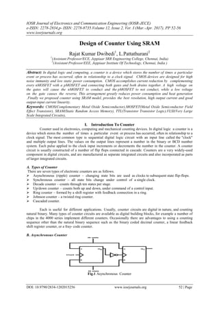
  • 1. IOSR Journal of Electronics and Communication Engineering (IOSR-JECE) e-ISSN: 2278-2834,p- ISSN: 2278-8735.Volume 12, Issue 2, Ver. I (Mar.-Apr. 2017), PP 52-56 www.iosrjournals.org DOI: 10.9790/2834-1202015256 www.iosrjournals.org 52 | Page Design of Counter Using SRAM Rajat Kumar Dwibedi1 , L.Pattathurani2 1 (Assistant Professor/ECE, Jeppiaar SRR Engineering College, Chennai, India) 2 (Assistant Professor/EEE, Jeppiaar Institute Of Technology, Chennai, India ) Abstract: In digital logic and computing, a counter is a device which stores the number of times a particular event or process has occurred, often in relationship to a clock signal. CMOS devices are designed for high noise immunity and low static power consumption. CMOS accomplishes current reduction by complementing every nMOSFET with a pMOSFET and connecting both gates and both drains together. A high voltage on the gates will cause the nMOSFET to conduct and the pMOSFET to not conduct, while a low voltage on the gate causes the reverse. This arrangement greatly reduces power consumption and heat generation .Finally we proposed counter using SRAM model, provides the best resolution, high output current and good output-input current linearity. Keywords: CMOS(Complementary Metal Oxide Semiconductor),MOSFET(Metal Oxide Semiconductor Field Effect Transistor), SRAM(Static Random Access Memory), TTL(Transistor Transistor Logic),VLSI(Very Large Scale Integrated Circuits). I. Introduction To Counter Counter used in electronics, computing and mechanical counting devices. In digital logic a counter is a device which stores the number of times a particular event or process has occurred, often in relationship to a clock signal. The most common type is sequential digital logic circuit with an input line called the "clock" and multiple output lines. The values on the output lines represent a number in the binary or BCD number system. Each pulse applied to the clock input increments or decrements the number in the counter. A counter circuit is usually constructed of a number of flip flops connected in cascade. Counters are a very widely-used component in digital circuits, and are manufactured as separate integrated circuits and also incorporated as parts of larger integrated circuits. A. Types of Counter There are seven types of electronic counters are as follows.  Asynchronous (ripple) counter – changing state bits are used as clocks to subsequent state flip-flops.  Synchronous counter – all state bits change under control of a single clock.  Decade counter – counts through ten states per stage.  Up/down counter – counts both up and down, under command of a control input.  Ring counter – formed by a shift register with feedback connection in a ring.  Johnson counter – a twisted ring counter.  Cascaded counter. Each is useful for different applications. Usually, counter circuits are digital in nature, and counting natural binary. Many types of counter circuits are available as digital building blocks, for example a number of chips in the 4000 series implement different counters. Occasionally there are advantages to using a counting sequence other than the natural binary sequence such as the binary coded decimal counter, a linear feedback shift register counter, or a fray- code counter. B. Asynchronous Counter Fig.1 Asynchronous Counter
  • 2. Design of Counter Using SRAM DOI: 10.9790/2834-1202015256 www.iosrjournals.org 53 | Page To add additional flip-flops, always inverting the output to its own input, and using the output from the previous flip-flop as the clock signal. The result is called a ripple counter, which can count to 2 n - 1 where n is the number of bits (flip-flop stages) in the counter. Ripple counters suffer from unstable outputs as the overflows "ripple" from stage to stage, but they do find frequent application as dividers for clock signals, where the instantaneous count is unimportant, but the division ratio overall is (to clarify this, a 1-bit counter is exactly equivalent to a divide by two circuit; the output frequency is exactly half that of the input when fed with a regular train of clock pulses).The use of flip-flop outputs as clocks leads to timing skew between the count data bits, making this ripple technique incompatible with normal synchronous circuit design styles. II. Existing System A. Conventional Counter Fig.2 Conventional Counter Counter built from four positive edge triggered d type flip flops connected in series. Clock pulses are fed into CLK input of FF0 whose output ,Q0 provides 2^0 output for flip flop 1 after 1 clock pulse the rising edge of the q bar output of each flip flop triggers the clock input of next flip flop at half the frequency of the clock pulses applied to its input. The Q outputs then represents a four bit binary count with Q0 to Q3 representing 2^0(1) to 2^3(8) respectively. Assuming that the four Q outputs are initially at 0000 ,the rising edge of the first clock pulse applied will cause the output Q0 to go to logic 1.the next clock pulse will make Q0 output return to logic 0,and at the same time Q0bar go from 0 to As Q0bar (and the clock input o flip flop 1 goes high ) this will now make Q1 high , indicating a value of 2^1 on the Q outputs . The next (third clock pulse will cause Q0 to go to logic 1 again, so both Q0 and Q1 will now be high , making the four bit output 1100.the fourth clock pulse will make both Q0and Q1 return to 0 and as Q1bar will go high at this time, this will toggle flip flop 2,making Q2 high and indicating 0010 at the outputs. Reading the output word from right to left ,the Q outputs therefore continue to represent a binary number equaling the number of input pulses received at the clock input of flip flop 0.as this is a four stage counter the flip flop will continue to toggle in sequence and the four Q outputs will output a sequence of binary values from 0000 to 1111, before the output returns to 0000. CMOS is a technology for constructing integrated circuits. CMOS technology is used in microprocessors, microcontrollers, static RAM, and other digital logic circuits. CMOS technology is also used for several analog circuits such as image sensors (CMOS sensor), data converters, and highly integrated transceivers for many types of communication. Two important characteristics of CMOS devices are high noise immunity and low static power consumption. Since one transistor of the pair is always off, the series combination draws significant power only momentarily during switching between on and off states. Consequently, CMOS devices do not produce as much waste heat as other forms of logic, for example transistor–transistor logic (TTL) or NMOS logic, which normally have some standing current even when not changing state. CMOS also allows a high density of logic functions on a chip. It was primarily for this reason that CMOS became the most used technology to be implemented in VLSI chips. CMOS circuits use a combination of p-type and n-type metal– oxide–semiconductor field-effect transistor (MOSFETs) to can be implemented with discrete devices for demonstrations, commercial CMOS products are integrated circuits composed of up to billions implement logic gates and other digital circuits. Although CMOS logic of transistors of both types, on a rectangular piece of silicon of between 10 and 400 mm 2 . III. Proposed System Static CMOS circuits are constructed in such a way that all PMOS transistors must have either an input from the voltage source or from another PMOS transistor. Similarly, all NMOS transistors must have either an input from ground or from another NMOS transistor. The composition of a PMOS transistor creates low resistance between its source and drain contacts when a low gate voltage is applied and high resistance when a high gate voltage is applied. On the other hand, the composition of an NMOS transistor creates high
  • 3. Design of Counter Using SRAM DOI: 10.9790/2834-1202015256 www.iosrjournals.org 54 | Page resistance between source and drain when a low gate voltage is applied and low resistance when a high gate voltage is applied. CMOS accomplishes current reduction by complementing every nMOSFET with a pMOSFET and connecting both gates and both drains together. A high voltage on the gates will cause the nMOSFET to conduct and the pMOSFET to not conduct, while a low voltage on the gates causes the reverse. This arrangement greatly reduces power consumption and heat generation. However, during the switching time, both MOSFETs conduct briefly as the gate voltage goes from one state to another. This induces a brief spike in power consumption and becomes a serious issue at high frequencies. In short, the outputs of the PMOS and NMOS transistors are complementary such that when the input is low, the output is high, and when the input is high, the output is low. Because of this behavior of input and output, the CMOS circuit's output is the inverse of the input. A. Counter using SRAM Fig.3 Counter using SRAM  In the above diagram there are totally 4 NMOS and 2 PMOS used. WL act as the reference line, BL and BL bar are the inputs. If BL=0 BL bar=1 whereas BL acts as the Vdd and BL bar act as the ground and vice versa as required. Q and Q bar are the outputs.  Q is given as the input M1 and M2 ,for which the output is obtained at Q bar which should be the complement of Q(Input).  Similarly, Q bar is given as the input to M3 and M 4 for which the output is taken from Q ,Which should be the complement of Q bar(input). B. Four Bit Counter Using SRAM Fig.4 4-bit Counter using SRAM
  • 4. Design of Counter Using SRAM DOI: 10.9790/2834-1202015256 www.iosrjournals.org 55 | Page The above diagram is the cascaded four bit counter using SRAM ,Where Q bar of one counter is given as input to the next counter. The principle of the matrix circuit is that if value of the pixel is higher than the value of reference of tension (Vr),the exit of the comparator is in a high state (5V). On the other hand, if value of the pixel is less than the value of the tension Vr, the exit of the comparator is in a low state (0V). After the comparison, the exits of the comparator are entered to the logical gating circuit AND. In the logical gating circuit AND, if signal comparator from line and row are 5V and corresponding LED is active. IV. Simulation Results And Discussions 4.1 Counter Using CMOS 4.2 Counter Using SRAM 4.3. Power Output for Existing System 4.4.Power output for Proposed System
  • 5. Design of Counter Using SRAM DOI: 10.9790/2834-1202015256 www.iosrjournals.org 56 | Page V. Conclusion In this paper we have designed a counter using a SRAM whereas previously the counter was designed using a D flip flop and CMOS in the existing system. In the proposed system the counter SRAM has a reduced power consumption when compared to that of the existing system ,since the transistors used in this system are connected in series, the power applied for the first transistor is used by all the succeeding transistors in the system .Also the use SRAM has many advantages such as Low hardware complexity, low cost for fabrication, mechanical flexibility, Strong optical absorption and efficient emission. References [1]. A high speed digital CMOS Divide-by-N frequency divider by S.Abdel-Hafeez,S Harb,W.Eisenstadt - 2008. [2]. A Digital CMOS parallel counter architecture based on state look- ahead logic‖ by S. Abdel- Hafez; A.Gordon-Ross -2011 . [ 3 ] . A digital CMOS parallel counter Architecture for frequency Divider Based on transmission Gate Logic by Anil Kumar Choudhary,K pitambar patra - 2014.