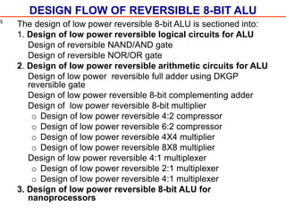
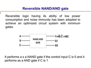
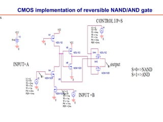
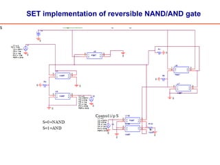
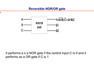
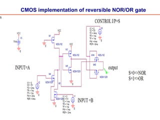
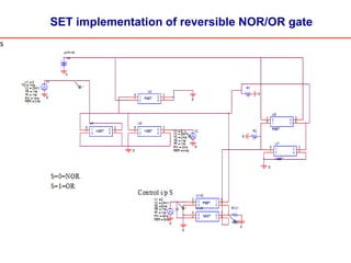
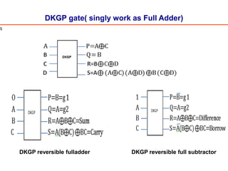
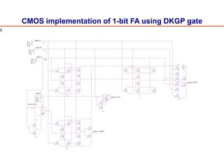
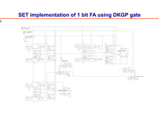
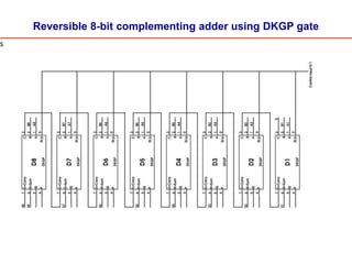
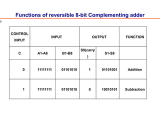
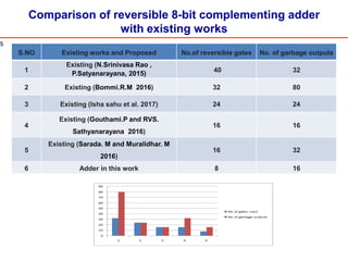
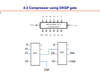
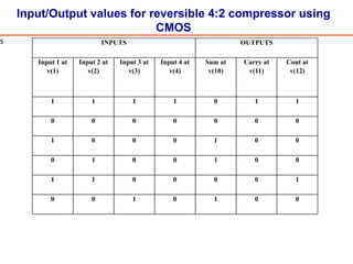
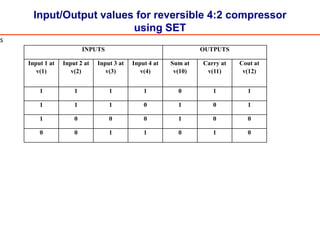
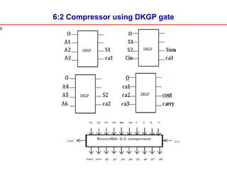
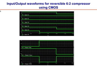
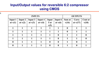
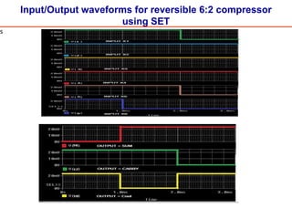
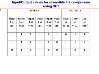
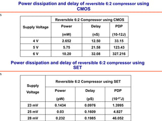
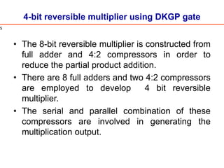
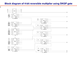
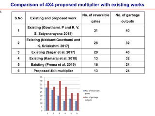
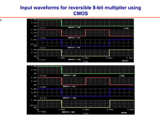
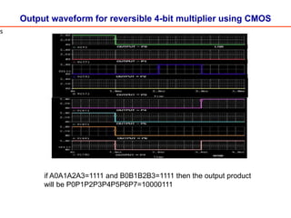
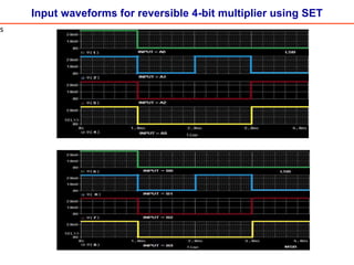
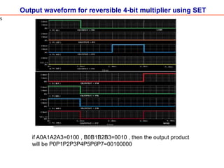
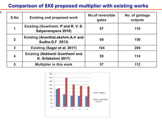
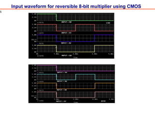
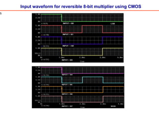
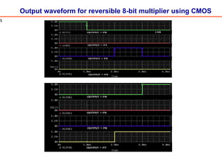
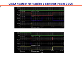
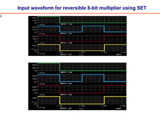
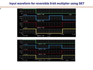
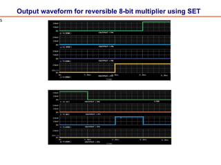
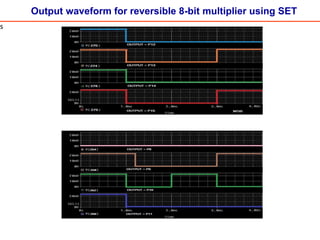
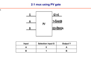
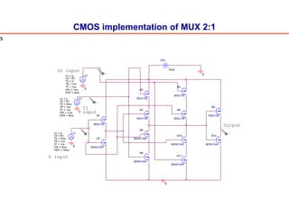
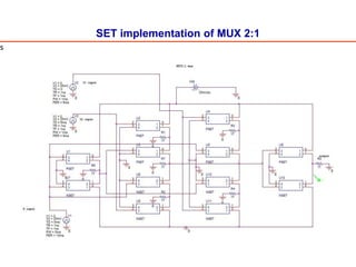
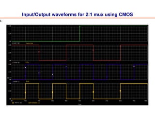
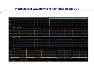
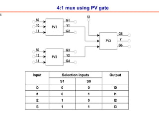
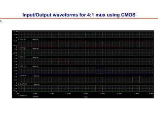
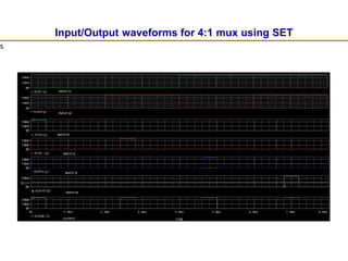
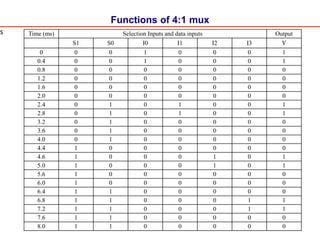
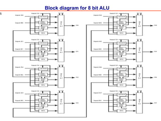
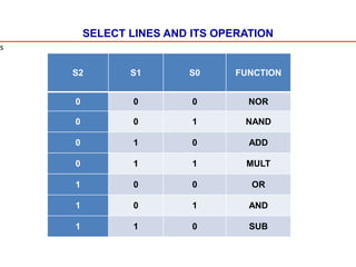
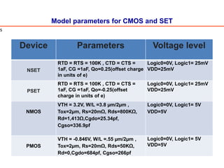
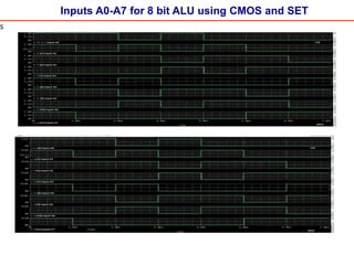
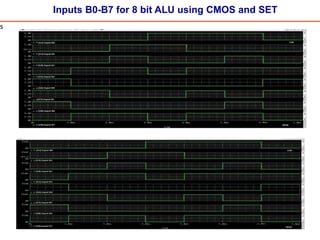
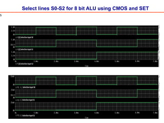
Computer assisted decision support system for
anomaly detection in EEG Signals
BY
Dr. AMIRTHALAKSHMI T M
Assistant Professor
Department of CSE
SRM Of Science And Technology
Ramapuram
Chennai-600089
SINGLE ELECTRON TRANSISTOR
1
DESIGN FLOW OF REVERSIBLE 8-BIT ALU
The design of low power reversible 8-bit ALU is sectioned into:
1. Design of low power reversible logical circuits for ALU
Design of reversible NAND/AND gate
Design of reversible NOR/OR gate
2. Design of low power reversible arithmetic circuits for ALU
Design of low power reversible full adder using DKGP
reversible gate
Design of low power reversible 8-bit complementing adder
Design of low power reversible 8-bit multiplier
o Design of low power reversible 4:2 compressor
o Design of low power reversible 6:2 compressor
o Design of low power reversible 4X4 multiplier
o Design of low power reversible 8X8 multiplier
Design of low power reversible 4:1 multiplexer
o Design of low power reversible 2:1 multiplexer
o Design of low power reversible 4:1 multiplexer
3. Design of low power reversible 8-bit ALU for
nanoprocessors
s
Reversible NAND/AND gate
It performs a s a NAND gate if the control input C is 0 and it
performs as a AND gate if C is 1.
s
Reversible logic having its ability of low power
consumption and noise immunity has been adopted to
achieve an optimized circuit system with minimum
gates.
CMOS implementation of reversible NAND/AND gate
s
SET implementation of reversible NAND/AND gate
s
Reversible NOR/OR gate
It performs a s a NOR gate if the control input C is 0 and it
performs as a OR gate if C is 1.
s
CMOS implementation of reversible NOR/OR gate
s
SET implementation of reversible NOR/OR gate
s
DKGP gate( singly work as Full Adder)
DKGP reversible fulladder DKGP reversible full subtractor
s
CMOS implementation of 1-bit FA using DKGP gate
VCC
M26
M2SJ102
input A
M30
M2SJ102
M39
M2SJ102
output P= B
V
M21
M2SK1044
M32
M2SK1044
M5
M2SJ102
output Q= A
VCC
M45
M2SJ102
M29
M2SJ102
M43
M2SJ102
0
M3
M2SJ102
M17
M2SK1044
V4
TD = 1ms
TF = 1ns
PW = 1ms
PER = 2ms
V1 = 0
TR = 1ns
V2 = 5V
output SUM
V
M19
M2SK1044
M31
M2SJ102
M11
M2SJ102
M36
M2SJ102
VCC
V
M28
M2SK1044
M24
M2SJ102
M7
M2SK1044
M41
M2SJ102
M46
M2SK1044
V
M37
M2SK1044
M8
M2SK1044
M34
M2SK1044
M1
M2SJ102
V3
TD = 2ms
TF = 1ns
PW = 2ms
PER = 4ms
V1 = 0
TR = 1ns
V2 = 5V
V 0
0
V5
TD = 8ms
TF = 0
PW = 8ms
PER = 8ms
V1 = 0
TR = 0
V2 = 0
0
M35
M2SJ102
M33
M2SK1044
0
M6
M2SK1044
output CARRY
0
V1
5Vdc
V
M9
M2SK1044
0
M23
M2SJ102
V2
TD = 4ms
TF = 1ns
PW = 4ms
PER = 8ms
V1 = 0
TR = 1ns
V2 = 5V
M44
M2SK1029
input B
M38
M2SK1044
M2
M2SJ102
M40
M2SK1044
M22
M2SJ102
M14
M2SJ102
M27
M2SK1044
VCC
M42
M2SK1029
M10
M2SK1044
input 0
0
M18
M2SK1044
M4
M2SJ102
V
0
M13
M2SJ102
M12
M2SJ102
M15
M2SK1044
input C
0
M16
M2SK1044
V
0
M20
M2SK1044
M25
M2SJ102
s
SET implementation of 1 bit FA using DKGP gate
s
Reversible 8-bit complementing adder using DKGP gate
s
Functions of reversible 8-bit Complementing adder
CONTROL
INPUT
INPUT OUTPUT FUNCTION
C A1-A8 B1-B8
S9(carry
)
S1-S8
0 11111111 01101010 1 01101001 Addition
1 11111111 01101010 0 10010101 Subtraction
s
Comparison of reversible 8-bit complementing adder
with existing works
S.NO Existing works and Proposed No.of reversible gates No. of garbage outputs
1
Existing (N.Srinivasa Rao ,
P.Satyanarayana, 2015)
40 32
2 Existing (Bommi.R.M 2016) 32 80
3 Existing (Isha sahu et al. 2017) 24 24
4
Existing (Gouthami.P and RVS.
Sathyanarayana 2016)
16 16
5
Existing (Sarada. M and Muralidhar. M
2016)
16 32
6 Adder in this work 8 16
s
4:2 Compressor using DKGP gate
s
INPUTS OUTPUTS
Input 1 at
v(1)
Input 2 at
v(2)
Input 3 at
v(3)
Input 4 at
v(4)
Sum at
v(10)
Carry at
v(11)
Cout at
v(12)
1 1 1 1 0 1 1
0 0 0 0 0 0 0
1 0 0 0 1 0 0
0 1 0 0 1 0 0
1 1 0 0 0 0 1
0 0 1 0 1 0 0
Input/Output values for reversible 4:2 compressor using
CMOS
s
Input/Output values for reversible 4:2 compressor
using SET
INPUTS OUTPUTS
Input 1 at
v(1)
Input 2 at
v(2)
Input 3 at
v(3)
Input 4 at
v(4)
Sum at
v(10)
Carry at
v(11)
Cout at
v(12)
1 1 1 1 0 1 1
1 1 1 0 1 0 1
1 0 0 0 1 0 0
0 0 1 1 0 1 0
s
6:2 Compressor using DKGP gate
s
Input/Output waveforms for reversible 6:2 compressor
using CMOS
s
Input/Output values for reversible 6:2 compressor
using CMOS
INPUTS OUTPUTS
Input 1
at v(1)
Input 2
at v(2)
Input 3
at v(3)
Input 4
at v(4)
Input
5 at
v(5)
Input 6
at v(6)
Sum at
v(16)
Carry
at v(17)
Cout at
v(18)
1 1 1 1 1 1 0 1 1
1 1 1 1 1 1 0 1 1
1 1 1 1 1 0 1 1 0
1 1 1 1 1 0 1 1 0
0 1 1 1 0 0 1 0 1
0 1 1 1 0 0 1 0 1
s
Input/Output waveforms for reversible 6:2 compressor
using SET
s
Input/Output values for reversible 6:2 compressor
using SET
INPUTS OUTPUTS
Input
1 at
v(1)
Input
2 at
v(2)
Input
3 at
v(3)
Input
4 at
v(4)
Input
5 at
v(5)
Input
6 at
v(6)
Sum
at
v(16)
Carry
at
v(17)
Cout
at
v(18)
1 1 1 1 1 1 0 1 1
1 1 1 1 1 0 1 1 0
0 1 1 1 0 0 1 0 1
s
Power dissipation and delay of reversible 6:2 compressor using
CMOS
s
Power dissipation and delay of reversible 6:2 compressor using
SET
s
Supply
Voltage
Reversible 6:2 Compressor using SET
Power
(pW)
Delay
(pS)
PDP
(10-27J)
23 mV 0.1434 0.0976 1.3995
25 mV 0.03 0.1609 4.827
28 mV 0.232 0.1985 46.052
Supply Voltage
Reversible 6:2 Compressor using CMOS
Power
(mW)
Delay
(nS)
PDP
(10-12J)
4 V 2.652 12.50 33.15
5 V 5.75 21.58 123.43
6 V 10.20 32.08 327.216
4-bit reversible multiplier using DKGP gate
• The 8-bit reversible multiplier is constructed from
full adder and 4:2 compressors in order to
reduce the partial product addition.
• There are 8 full adders and two 4:2 compressors
are employed to develop 4 bit reversible
multiplier.
• The serial and parallel combination of these
compressors are involved in generating the
multiplication output.
s
Block diagram of 4-bit reversible multiplier using DKGP gate
s
Comparison of 4X4 proposed multiplier with existing works
s
S.No Existing and proposed work
No. of reversible
gates
No. of garbage
outputs
1
Existing (Gowthami. P and R. V.
S. Satyanarayana 2018)
31 40
2
Existing (NekkantiGowthami and
K. Srilakshmi 2017)
28 32
3 Existing (Sagar et al. 2017) 20 40
4 Existing (Kamaraj et al. 2018) 13 32
5 Existing (Prema et al. 2019) 16 24
6 Proposed 4bit multiplier 13 24
0
5
10
15
20
25
30
35
40
45
1 2 3 4 5 6
No. of reversible
gates
No. of garbage
outputs
Input waveforms for reversible 8-bit multiplier using
CMOS
s
Output waveform for reversible 4-bit multiplier using CMOS
s
if A0A1A2A3=1111 and B0B1B2B3=1111 then the output product
will be P0P1P2P3P4P5P6P7=10000111
Input waveforms for reversible 4-bit multiplier using SET
s
Output waveform for reversible 4-bit multiplier using SET
s
if A0A1A2A3=0100 , B0B1B2B3=0010 , then the output product
will be P0P1P2P3P4P5P6P7=00100000
8-bit reversible multiplier using DKGP gate
• The 8-bit reversible multiplier is constructed from
4:2 and 6:2 compressors in order to reduce the
partial product addition.
• There are 22 full adders, eight 4:2 compressors
and five 6:2 compressors are employed to
develop reversible multiplier.
• The serial and parallel combination of these
compressors are involved in generating the
multiplication output.
s
Block diagram of 8-bit reversible multiplier using DKGP gate
s
Comparison of 8X8 proposed multiplier with existing works
S.No Existing and proposed work
No.of reversible
gates
No. of garbage
outputs
1
Existing (Gowthami. P and R. V. S.
Satyanarayana 2018)
97 116
2
Existing (AnanthaLakshmi.A,V and
Sudha.G.F 2013)
69 159
3 Existing (Sagar et al. 2017) 104 208
4
Existing (Nekkanti Gowthami and
K. Srilakshmi 2017)
59 114
5 Multiplier in this work 57 112
s
Input waveform for reversible 8-bit multiplier using CMOS
s
Input waveform for reversible 8-bit multiplier using CMOS
s
Output waveform for reversible 8-bit multiplier using CMOS
s
Output waveform for reversible 8-bit multiplier using CMOS
s
Input waveform for reversible 8-bit multiplier using SET
s
Input waveform for reversible 8-bit multiplier using SET
s
Output waveform for reversible 8-bit multiplier using SET
s
Output waveform for reversible 8-bit multiplier using SET
s
2:1 mux using PV gate
s
Input Selection input S Output Y
A 0 A
B 1 B
CMOS implementation of MUX 2:1
0
V
M7
M2SK1044
0
I1
input
M12
M2SK1044
M5
M2SJ102
V1
TD = 5ms
TF = 1ns
PW = 5ms
PER = 10ms
V1 = 0
TR = 1ns
V2 = 5V
0
M10
M2SK1044
Output
Vdd
5Vdc
V3
TD = 6ms
TF = 1ns
PW = 1ms
PER = 9ms
V1 = 0
TR = 1ns
V2 = 5V
V
M2
M2SJ102
M3
M2SJ102
M8
M2SK1044
M1
M2SJ102
V
V
V2
TD = 0
TF = 1ns
PW = 1ms
PER = 9ms
V1 = 0
TR = 1ns
V2 = 5V
M11
M2SK1044
0
I0 input
M9
M2SK1044
M4
M2SJ102
0
S input
M6
M2SJ102
s
SET implementation of MUX 2:1
s
Input/Output waveforms for 2:1 mux using CMOS
s
Input/Output waveforms for 2:1 mux using SET
s
4:1 mux using PV gate
s
Input Selection inputs Output
S1 S0
I0 0 0 I0
I1 0 1 I1
I2 1 0 I2
I3 1 1 I3
Input/Output waveforms for 4:1 mux using CMOS
s
Input/Output waveforms for 4:1 mux using SET
s
Functions of 4:1 mux
Time (ms) Selection Inputs and data inputs Output
S1 S0 I0 I1 I2 I3 Y
0 0 0 1 0 0 0 1
0.4 0 0 1 0 0 0 1
0.8 0 0 0 0 0 0 0
1.2 0 0 0 0 0 0 0
1.6 0 0 0 0 0 0 0
2.0 0 0 0 0 0 0 0
2.4 0 1 0 1 0 0 1
2.8 0 1 0 1 0 0 1
3.2 0 1 0 0 0 0 0
3.6 0 1 0 0 0 0 0
4.0 0 1 0 0 0 0 0
4.4 1 0 0 0 0 0 0
4.6 1 0 0 0 1 0 1
5.0 1 0 0 0 1 0 1
5.6 1 0 0 0 0 0 0
6.0 1 0 0 0 0 0 0
6.4 1 1 0 0 0 0 0
6.8 1 1 0 0 0 1 1
7.2 1 1 0 0 0 1 1
7.6 1 1 0 0 0 0 0
8.0 1 1 0 0 0 0 0
s
Block diagram for 8 bit ALU
s
SELECT LINES AND ITS OPERATION
S2 S1 S0 FUNCTION
0 0 0 NOR
0 0 1 NAND
0 1 0 ADD
0 1 1 MULT
1 0 0 OR
1 0 1 AND
1 1 0 SUB
s
Model parameters for CMOS and SET
Device Parameters Voltage level
NSET
RTD = RTS = 100K , CTD = CTS =
1aF, CG =1aF, Qo=0.25(offset charge
in units of e)
Logic0=0V, Logic1= 25mV
VDD=25mV
PSET
RTD = RTS = 100K , CTD = CTS =
1aF, CG =1aF, Qo=-0.25(offset
charge in units of e)
Logic0=0V, Logic1= 25mV
VDD=25mV
NMOS
VTH = 3.2V, W/L =3.8 µm/2µm ,
Tox=2µm, Rs=20mΩ, Rds=800KΩ,
Rd=1,413Ω,Cgdo=25.34pf,
Cgso=336.9pf
Logic0=0V, Logic1= 5V
VDD=5V
PMOS
VTH = -0.846V, W/L =.55 µm/2µm ,
Tox=2µm, Rs=20mΩ, Rds=50KΩ,
Rd=0,Cgdo=684pf, Cgso=266pf
Logic0=0V, Logic1= 5V
VDD=5V
s
Inputs A0-A7 for 8 bit ALU using CMOS and SET
s
Inputs B0-B7 for 8 bit ALU using CMOS and SET
s
Select lines S0-S2 for 8 bit ALU using CMOS and SET
s
Outputs O0-O7 for 8 bit ALU using CMOS and SET
s
INPUTS/OUTPUTS OF 8 BIT ALU
CONTROL INPUTS INPUT OUTPUT FUNCTION
S2 S1 S0 A0-A7 B0-B7 O0-O7
0 0 0
11101101 00001110 O0-O7 NOR
0 0 1
10100100 00010101 00010000 NAND
0 1 0
01101010 01110001 11111011 ADDITION
0 1 1
10010100 11000000 00100111 MUL
1 0 0
01100110 10010101 11011110 OR
1 0 1
00110011 10110011 11110111 AND
1 1 0
00011101 00011100 00110011 SUB
s
Conclusion
• The SET based ALU outperforms the conventional
CMOS based ALU in terms of power, delay and
power delay product. The SET technology provides
the same output response for the same input signal
frequency as in CMOS with very low operating
voltage.
• This work witnessed that the SET technology
provides an alternative approach to conventional
CMOS in low power digital applications.
• Therefore ALU using SET could be a potential
towards the development of faster nanoprocessor
with smaller size and ultra low power consumption..
71
s
Future Scope
• The sequential circuits can be developed using SET. The
research work has stopped at the simulation itself. The
practical implementation of SET can be done with adequate
nanolithographic techniques and parameter dispersion
considerations.
• Laptops, implanted medical devices, wearable computers,
wallet smart cards are some of the applications with SET
based reversible subtractors.
• Unmanned vehicles need to perform object detection,
classification, segmentation and so on. More number of
iterations will be required. Thus the processor with SET
based ALU will be very much required to dissipate ultra low
power.
• Battery operated vehicles require low voltage operated
circuit systems where the low power SET based circuit
systems will be helpful.
72
REFERENCES
73
[1] T. Esther Rani, M.A. Rani and R. Rao, “AREA optimized low power
arithmetic and logic unit,” IEEE International Conference on Electronics
Computer Technology, April 2011, pp. 224–228.
[2] Landauer. R., “Irreversibility and Heat Generation in the Computing
Process”, IBM J. Research and Development, vol. 3, pp. 183- 191, 1961.
[3] Bennett. C.H., “Logical reversibility of computation”, IBM Journal
Research and Development, volume 17, pp. 525-532, 1973.
[4] K. Uchida, K. Matsuzawa, J. Koga, R. Ohba, S. Takagi and A. Toriumi,
“Analytical Single-Electron Transistor (SET) Model for Design and Analysis of
Realistic SET Circuits,” Japanese Journal of Applied Physics, Vol. 39, No. 4B,
2000, pp. 2321-2324. doi:10.1143/JJAP.39.2321
[5] H. Inokawa and Y. Takahashi, “A Compact Analytical Model for Asymmetric
Single-Electron Tunneling Tran-sistors,” IEEE Transactions on Electron
Devices, Vol. 50, No. 2, 2003, pp. 455-461. doi:10.1109/TED.2002.808554
[6] S. Mahapatra, V. Vaish, C. Wasshuber, K. Banerjee and A. M. Ionescu,
“Analytical Modeling of Single Electron Transistor for Hybrid CMOS-SET
Analog IC Design,” IEEE Transactions on Electron Devices, Vol. 51, No. 11,
2004, pp. 1772-1782. doi:10.1109/TED.2004.837369
74
[7]Dubuc. C., Beaumont. A., Beauvais. J. and Drouin. D., “Current
Conduction Models in the High Temperature Single-Electron Transistor,”
Solid-State lectronics, Vol.53, No. 5, pp. 478-482, 2009.
[9] Frans Willy and Yudi Darma ,” Modeling and simulation of single electron
transistor with master equation approach”, Journal of Physics:
Conference Series, Volume 739, Number 1,2016.
[10]Gangadhar Reddy Ramireddy “A Novel Power-Aware and High
Performance Full Adder Cell for Ultra low Power Design,” IEEE
International Conference on Circuit, Power and Computing Technologies,
2014, pp. 1121-1126.
[11]JVR Ravindra, Gangadhar Reddy Ramireddy and Harikrishna
Kamatham, “Design of Ultra Low Power Full Adder using Modified Branch
Based Logic Style,” IEEE European Modelling Symposium, 2013, pp.
691-696.
[12] Rajesh Parihar, Nidhi Tiwari, Aditya Mandloi and Dr.Binod Kumar, “An
Implementation of 1-Bit Low Power Full Adder Based on Multiplexer and
Pass Transistor Logic,” IEEE International Conference on Information
Communication and Embedded System, 2014, pp. 101- 103.
[13]L. Dhulipalla and A. Deepak, “Design and implementation Of 4-bit ALU
using FINFETS for nano scaletechnology,” IEEE International Conference
on Nanoscience, Engineering and Technology , November 2011, pp. 190–
195.
75
[14] A. Srivastava and C. Srinivasan, “ALU Design Using Reconfigurable
CMOS Logic,” IEEE 45th midwest symposium on circuit and system, vol.
2, August 2002, pp. 663-6.
[15] Ravi Tiwari and Khemraj Deshmukh, “Design and analysis of low
power 11-transistor full adder,” IJAREEIE, vol. 3, issue 6, June 2014,pp.
10301-10307.
[16] Pooja Vaishnav and Mr.Vishal Moyal, “Performance Analysis Of 8-Bit
ALU For Power In 32 Nm Scale,” IJERT, vol. 1, issue 8, October 2012
pp. 1-3.
[17] S. Usha, M. Rajendren, A.Kavitha,”Low power area efficient ALU with
low power full adder”,IEEE conference on Computing for sustainable
global development,2016.
[18] Biswabandhu Jana, Anindya Jana, Subhramita Basak, Jamuna Kanta
Sing, Subir Kumar Sarkar,” Design and Performance Analysis of
Reversible Logic based ALU using Hybrid Single Electron
Transistor”,IEEE RAECS UIET Panjab University Chandigarh,2014.
[19] Anitesh Sharma, Ravi Tiwari,” Low Power 8-bit ALU Design Using Full
Adder and Multiplexer”, IEEE WiSPNET , 2016
[20] Anindya Jana, N Basanta Sing, Jamuna K Sing and Subir Kumar Sarkar
,“Design and simulation of hybrid CMOS SET circuits”, Microelectronics
Reliability, Elseveier, Vol. 53, pp. 592-599, Issue 4, April 2013.
[21] Biswabandhu Jana, Anindya Jana, Jamuna Kanta Sing, and Subir
Kumar Sarkar, “A Comparative Performance Study of Hybrid SET-CMOS
Based Logic Circuits for the Estimation of Robustness” Journal of Nano
and Electronic Physics, Vol. 5 No. 3, pp. 54-57, 2013.
[23] Gouthami.P and RVS. Sathyanarayana, "Design of digital adder using
Reversible logic", International journal of engineering research and
applications,Vol 6, Issue 6, pp 53-57, 2016.
[24] Sarada. M and Muralidhar. M , "A novel design and implementation of
reversible adder cum subtractor", International journal of innovative in
engineering and technology, special issue on ETICE 16, pp 48-54, 2016.
[25] Y. Taur, D. A. Buchanan, W. Chen, D. Frank, K. Ismail, S. Lo, G.Sai-
Halasz, R. Viswanathan, H. Wann, S. Wind, and H. Wong, “CMOS
scaling into the nanometer regime,” Proc. IEEE, vol. 85, no. 4, pp. 486–
504, Apr. 1997
[26] K. K. Likharev, “Single-electron devices and their applications,”
Proc.IEEE, vol. 87, no. 4, pp. 606–632, Apr. 1999.
76
77
[28] AnanthaLakshmi.A,V and Sudha.G.F, "An Efficient Implementation
of a Reversible Single Precision Floating Point Multiplier Using 4:3
Compressor", Elsevier, Proc. of Int. Conf. on Advances in
Information Technology and Mobile Communication, pp 229-238,
2013.
[29] Sagar, K Suresh Babu, " Design of Low Power Vedic Multiplier
Based on Reversible Logic", Int. Journal of Engineering Research
and Application ISSN : 2248-9622, Vol. 7, Issue 3, ( Part -2) , pp.73-
78, 2017.
[30] Nekkanti Gowthami and K. Srilakshmi, " Design and
mplementation of Reversible Multiplier using optimum TG Full
Adder". IOSR Journal of Electronics and Communication
Engineering (IOSR-JECE), Vol 12, Issue 3, Pp 81-89, 2017
THANK YOU
78

Single elctron transisto PHASE 2.pptx

  • 1.
    Computer assisted decisionsupport system for anomaly detection in EEG Signals BY Dr. AMIRTHALAKSHMI T M Assistant Professor Department of CSE SRM Of Science And Technology Ramapuram Chennai-600089 SINGLE ELECTRON TRANSISTOR 1
  • 2.
    DESIGN FLOW OFREVERSIBLE 8-BIT ALU The design of low power reversible 8-bit ALU is sectioned into: 1. Design of low power reversible logical circuits for ALU Design of reversible NAND/AND gate Design of reversible NOR/OR gate 2. Design of low power reversible arithmetic circuits for ALU Design of low power reversible full adder using DKGP reversible gate Design of low power reversible 8-bit complementing adder Design of low power reversible 8-bit multiplier o Design of low power reversible 4:2 compressor o Design of low power reversible 6:2 compressor o Design of low power reversible 4X4 multiplier o Design of low power reversible 8X8 multiplier Design of low power reversible 4:1 multiplexer o Design of low power reversible 2:1 multiplexer o Design of low power reversible 4:1 multiplexer 3. Design of low power reversible 8-bit ALU for nanoprocessors s
  • 3.
    Reversible NAND/AND gate Itperforms a s a NAND gate if the control input C is 0 and it performs as a AND gate if C is 1. s Reversible logic having its ability of low power consumption and noise immunity has been adopted to achieve an optimized circuit system with minimum gates.
  • 4.
    CMOS implementation ofreversible NAND/AND gate s
  • 5.
    SET implementation ofreversible NAND/AND gate s
  • 6.
    Reversible NOR/OR gate Itperforms a s a NOR gate if the control input C is 0 and it performs as a OR gate if C is 1. s
  • 7.
    CMOS implementation ofreversible NOR/OR gate s
  • 8.
    SET implementation ofreversible NOR/OR gate s
  • 9.
    DKGP gate( singlywork as Full Adder) DKGP reversible fulladder DKGP reversible full subtractor s
  • 10.
    CMOS implementation of1-bit FA using DKGP gate VCC M26 M2SJ102 input A M30 M2SJ102 M39 M2SJ102 output P= B V M21 M2SK1044 M32 M2SK1044 M5 M2SJ102 output Q= A VCC M45 M2SJ102 M29 M2SJ102 M43 M2SJ102 0 M3 M2SJ102 M17 M2SK1044 V4 TD = 1ms TF = 1ns PW = 1ms PER = 2ms V1 = 0 TR = 1ns V2 = 5V output SUM V M19 M2SK1044 M31 M2SJ102 M11 M2SJ102 M36 M2SJ102 VCC V M28 M2SK1044 M24 M2SJ102 M7 M2SK1044 M41 M2SJ102 M46 M2SK1044 V M37 M2SK1044 M8 M2SK1044 M34 M2SK1044 M1 M2SJ102 V3 TD = 2ms TF = 1ns PW = 2ms PER = 4ms V1 = 0 TR = 1ns V2 = 5V V 0 0 V5 TD = 8ms TF = 0 PW = 8ms PER = 8ms V1 = 0 TR = 0 V2 = 0 0 M35 M2SJ102 M33 M2SK1044 0 M6 M2SK1044 output CARRY 0 V1 5Vdc V M9 M2SK1044 0 M23 M2SJ102 V2 TD = 4ms TF = 1ns PW = 4ms PER = 8ms V1 = 0 TR = 1ns V2 = 5V M44 M2SK1029 input B M38 M2SK1044 M2 M2SJ102 M40 M2SK1044 M22 M2SJ102 M14 M2SJ102 M27 M2SK1044 VCC M42 M2SK1029 M10 M2SK1044 input 0 0 M18 M2SK1044 M4 M2SJ102 V 0 M13 M2SJ102 M12 M2SJ102 M15 M2SK1044 input C 0 M16 M2SK1044 V 0 M20 M2SK1044 M25 M2SJ102 s
  • 11.
    SET implementation of1 bit FA using DKGP gate s
  • 12.
    Reversible 8-bit complementingadder using DKGP gate s
  • 13.
    Functions of reversible8-bit Complementing adder CONTROL INPUT INPUT OUTPUT FUNCTION C A1-A8 B1-B8 S9(carry ) S1-S8 0 11111111 01101010 1 01101001 Addition 1 11111111 01101010 0 10010101 Subtraction s
  • 14.
    Comparison of reversible8-bit complementing adder with existing works S.NO Existing works and Proposed No.of reversible gates No. of garbage outputs 1 Existing (N.Srinivasa Rao , P.Satyanarayana, 2015) 40 32 2 Existing (Bommi.R.M 2016) 32 80 3 Existing (Isha sahu et al. 2017) 24 24 4 Existing (Gouthami.P and RVS. Sathyanarayana 2016) 16 16 5 Existing (Sarada. M and Muralidhar. M 2016) 16 32 6 Adder in this work 8 16 s
  • 15.
  • 16.
    INPUTS OUTPUTS Input 1at v(1) Input 2 at v(2) Input 3 at v(3) Input 4 at v(4) Sum at v(10) Carry at v(11) Cout at v(12) 1 1 1 1 0 1 1 0 0 0 0 0 0 0 1 0 0 0 1 0 0 0 1 0 0 1 0 0 1 1 0 0 0 0 1 0 0 1 0 1 0 0 Input/Output values for reversible 4:2 compressor using CMOS s
  • 17.
    Input/Output values forreversible 4:2 compressor using SET INPUTS OUTPUTS Input 1 at v(1) Input 2 at v(2) Input 3 at v(3) Input 4 at v(4) Sum at v(10) Carry at v(11) Cout at v(12) 1 1 1 1 0 1 1 1 1 1 0 1 0 1 1 0 0 0 1 0 0 0 0 1 1 0 1 0 s
  • 18.
  • 19.
    Input/Output waveforms forreversible 6:2 compressor using CMOS s
  • 20.
    Input/Output values forreversible 6:2 compressor using CMOS INPUTS OUTPUTS Input 1 at v(1) Input 2 at v(2) Input 3 at v(3) Input 4 at v(4) Input 5 at v(5) Input 6 at v(6) Sum at v(16) Carry at v(17) Cout at v(18) 1 1 1 1 1 1 0 1 1 1 1 1 1 1 1 0 1 1 1 1 1 1 1 0 1 1 0 1 1 1 1 1 0 1 1 0 0 1 1 1 0 0 1 0 1 0 1 1 1 0 0 1 0 1 s
  • 21.
    Input/Output waveforms forreversible 6:2 compressor using SET s
  • 22.
    Input/Output values forreversible 6:2 compressor using SET INPUTS OUTPUTS Input 1 at v(1) Input 2 at v(2) Input 3 at v(3) Input 4 at v(4) Input 5 at v(5) Input 6 at v(6) Sum at v(16) Carry at v(17) Cout at v(18) 1 1 1 1 1 1 0 1 1 1 1 1 1 1 0 1 1 0 0 1 1 1 0 0 1 0 1 s
  • 23.
    Power dissipation anddelay of reversible 6:2 compressor using CMOS s Power dissipation and delay of reversible 6:2 compressor using SET s Supply Voltage Reversible 6:2 Compressor using SET Power (pW) Delay (pS) PDP (10-27J) 23 mV 0.1434 0.0976 1.3995 25 mV 0.03 0.1609 4.827 28 mV 0.232 0.1985 46.052 Supply Voltage Reversible 6:2 Compressor using CMOS Power (mW) Delay (nS) PDP (10-12J) 4 V 2.652 12.50 33.15 5 V 5.75 21.58 123.43 6 V 10.20 32.08 327.216
  • 24.
    4-bit reversible multiplierusing DKGP gate • The 8-bit reversible multiplier is constructed from full adder and 4:2 compressors in order to reduce the partial product addition. • There are 8 full adders and two 4:2 compressors are employed to develop 4 bit reversible multiplier. • The serial and parallel combination of these compressors are involved in generating the multiplication output. s
  • 25.
    Block diagram of4-bit reversible multiplier using DKGP gate s
  • 26.
    Comparison of 4X4proposed multiplier with existing works s S.No Existing and proposed work No. of reversible gates No. of garbage outputs 1 Existing (Gowthami. P and R. V. S. Satyanarayana 2018) 31 40 2 Existing (NekkantiGowthami and K. Srilakshmi 2017) 28 32 3 Existing (Sagar et al. 2017) 20 40 4 Existing (Kamaraj et al. 2018) 13 32 5 Existing (Prema et al. 2019) 16 24 6 Proposed 4bit multiplier 13 24 0 5 10 15 20 25 30 35 40 45 1 2 3 4 5 6 No. of reversible gates No. of garbage outputs
  • 27.
    Input waveforms forreversible 8-bit multiplier using CMOS s
  • 28.
    Output waveform forreversible 4-bit multiplier using CMOS s if A0A1A2A3=1111 and B0B1B2B3=1111 then the output product will be P0P1P2P3P4P5P6P7=10000111
  • 29.
    Input waveforms forreversible 4-bit multiplier using SET s
  • 30.
    Output waveform forreversible 4-bit multiplier using SET s if A0A1A2A3=0100 , B0B1B2B3=0010 , then the output product will be P0P1P2P3P4P5P6P7=00100000
  • 31.
    8-bit reversible multiplierusing DKGP gate • The 8-bit reversible multiplier is constructed from 4:2 and 6:2 compressors in order to reduce the partial product addition. • There are 22 full adders, eight 4:2 compressors and five 6:2 compressors are employed to develop reversible multiplier. • The serial and parallel combination of these compressors are involved in generating the multiplication output. s
  • 32.
    Block diagram of8-bit reversible multiplier using DKGP gate s
  • 33.
    Comparison of 8X8proposed multiplier with existing works S.No Existing and proposed work No.of reversible gates No. of garbage outputs 1 Existing (Gowthami. P and R. V. S. Satyanarayana 2018) 97 116 2 Existing (AnanthaLakshmi.A,V and Sudha.G.F 2013) 69 159 3 Existing (Sagar et al. 2017) 104 208 4 Existing (Nekkanti Gowthami and K. Srilakshmi 2017) 59 114 5 Multiplier in this work 57 112 s
  • 34.
    Input waveform forreversible 8-bit multiplier using CMOS s
  • 35.
    Input waveform forreversible 8-bit multiplier using CMOS s
  • 36.
    Output waveform forreversible 8-bit multiplier using CMOS s
  • 37.
    Output waveform forreversible 8-bit multiplier using CMOS s
  • 38.
    Input waveform forreversible 8-bit multiplier using SET s
  • 39.
    Input waveform forreversible 8-bit multiplier using SET s
  • 40.
    Output waveform forreversible 8-bit multiplier using SET s
  • 41.
    Output waveform forreversible 8-bit multiplier using SET s
  • 42.
    2:1 mux usingPV gate s Input Selection input S Output Y A 0 A B 1 B
  • 43.
    CMOS implementation ofMUX 2:1 0 V M7 M2SK1044 0 I1 input M12 M2SK1044 M5 M2SJ102 V1 TD = 5ms TF = 1ns PW = 5ms PER = 10ms V1 = 0 TR = 1ns V2 = 5V 0 M10 M2SK1044 Output Vdd 5Vdc V3 TD = 6ms TF = 1ns PW = 1ms PER = 9ms V1 = 0 TR = 1ns V2 = 5V V M2 M2SJ102 M3 M2SJ102 M8 M2SK1044 M1 M2SJ102 V V V2 TD = 0 TF = 1ns PW = 1ms PER = 9ms V1 = 0 TR = 1ns V2 = 5V M11 M2SK1044 0 I0 input M9 M2SK1044 M4 M2SJ102 0 S input M6 M2SJ102 s
  • 44.
  • 45.
    Input/Output waveforms for2:1 mux using CMOS s
  • 46.
    Input/Output waveforms for2:1 mux using SET s
  • 47.
    4:1 mux usingPV gate s Input Selection inputs Output S1 S0 I0 0 0 I0 I1 0 1 I1 I2 1 0 I2 I3 1 1 I3
  • 48.
    Input/Output waveforms for4:1 mux using CMOS s
  • 49.
    Input/Output waveforms for4:1 mux using SET s
  • 50.
    Functions of 4:1mux Time (ms) Selection Inputs and data inputs Output S1 S0 I0 I1 I2 I3 Y 0 0 0 1 0 0 0 1 0.4 0 0 1 0 0 0 1 0.8 0 0 0 0 0 0 0 1.2 0 0 0 0 0 0 0 1.6 0 0 0 0 0 0 0 2.0 0 0 0 0 0 0 0 2.4 0 1 0 1 0 0 1 2.8 0 1 0 1 0 0 1 3.2 0 1 0 0 0 0 0 3.6 0 1 0 0 0 0 0 4.0 0 1 0 0 0 0 0 4.4 1 0 0 0 0 0 0 4.6 1 0 0 0 1 0 1 5.0 1 0 0 0 1 0 1 5.6 1 0 0 0 0 0 0 6.0 1 0 0 0 0 0 0 6.4 1 1 0 0 0 0 0 6.8 1 1 0 0 0 1 1 7.2 1 1 0 0 0 1 1 7.6 1 1 0 0 0 0 0 8.0 1 1 0 0 0 0 0 s
  • 51.
    Block diagram for8 bit ALU s
  • 52.
    SELECT LINES ANDITS OPERATION S2 S1 S0 FUNCTION 0 0 0 NOR 0 0 1 NAND 0 1 0 ADD 0 1 1 MULT 1 0 0 OR 1 0 1 AND 1 1 0 SUB s
  • 53.
    Model parameters forCMOS and SET Device Parameters Voltage level NSET RTD = RTS = 100K , CTD = CTS = 1aF, CG =1aF, Qo=0.25(offset charge in units of e) Logic0=0V, Logic1= 25mV VDD=25mV PSET RTD = RTS = 100K , CTD = CTS = 1aF, CG =1aF, Qo=-0.25(offset charge in units of e) Logic0=0V, Logic1= 25mV VDD=25mV NMOS VTH = 3.2V, W/L =3.8 µm/2µm , Tox=2µm, Rs=20mΩ, Rds=800KΩ, Rd=1,413Ω,Cgdo=25.34pf, Cgso=336.9pf Logic0=0V, Logic1= 5V VDD=5V PMOS VTH = -0.846V, W/L =.55 µm/2µm , Tox=2µm, Rs=20mΩ, Rds=50KΩ, Rd=0,Cgdo=684pf, Cgso=266pf Logic0=0V, Logic1= 5V VDD=5V s
  • 54.
    Inputs A0-A7 for8 bit ALU using CMOS and SET s
  • 55.
    Inputs B0-B7 for8 bit ALU using CMOS and SET s
  • 56.
    Select lines S0-S2for 8 bit ALU using CMOS and SET s
  • 57.
    Outputs O0-O7 for8 bit ALU using CMOS and SET s
  • 58.
    INPUTS/OUTPUTS OF 8BIT ALU CONTROL INPUTS INPUT OUTPUT FUNCTION S2 S1 S0 A0-A7 B0-B7 O0-O7 0 0 0 11101101 00001110 O0-O7 NOR 0 0 1 10100100 00010101 00010000 NAND 0 1 0 01101010 01110001 11111011 ADDITION 0 1 1 10010100 11000000 00100111 MUL 1 0 0 01100110 10010101 11011110 OR 1 0 1 00110011 10110011 11110111 AND 1 1 0 00011101 00011100 00110011 SUB s
  • 59.
    Conclusion • The SETbased ALU outperforms the conventional CMOS based ALU in terms of power, delay and power delay product. The SET technology provides the same output response for the same input signal frequency as in CMOS with very low operating voltage. • This work witnessed that the SET technology provides an alternative approach to conventional CMOS in low power digital applications. • Therefore ALU using SET could be a potential towards the development of faster nanoprocessor with smaller size and ultra low power consumption.. 71 s
  • 60.
    Future Scope • Thesequential circuits can be developed using SET. The research work has stopped at the simulation itself. The practical implementation of SET can be done with adequate nanolithographic techniques and parameter dispersion considerations. • Laptops, implanted medical devices, wearable computers, wallet smart cards are some of the applications with SET based reversible subtractors. • Unmanned vehicles need to perform object detection, classification, segmentation and so on. More number of iterations will be required. Thus the processor with SET based ALU will be very much required to dissipate ultra low power. • Battery operated vehicles require low voltage operated circuit systems where the low power SET based circuit systems will be helpful. 72
  • 61.
    REFERENCES 73 [1] T. EstherRani, M.A. Rani and R. Rao, “AREA optimized low power arithmetic and logic unit,” IEEE International Conference on Electronics Computer Technology, April 2011, pp. 224–228. [2] Landauer. R., “Irreversibility and Heat Generation in the Computing Process”, IBM J. Research and Development, vol. 3, pp. 183- 191, 1961. [3] Bennett. C.H., “Logical reversibility of computation”, IBM Journal Research and Development, volume 17, pp. 525-532, 1973. [4] K. Uchida, K. Matsuzawa, J. Koga, R. Ohba, S. Takagi and A. Toriumi, “Analytical Single-Electron Transistor (SET) Model for Design and Analysis of Realistic SET Circuits,” Japanese Journal of Applied Physics, Vol. 39, No. 4B, 2000, pp. 2321-2324. doi:10.1143/JJAP.39.2321 [5] H. Inokawa and Y. Takahashi, “A Compact Analytical Model for Asymmetric Single-Electron Tunneling Tran-sistors,” IEEE Transactions on Electron Devices, Vol. 50, No. 2, 2003, pp. 455-461. doi:10.1109/TED.2002.808554 [6] S. Mahapatra, V. Vaish, C. Wasshuber, K. Banerjee and A. M. Ionescu, “Analytical Modeling of Single Electron Transistor for Hybrid CMOS-SET Analog IC Design,” IEEE Transactions on Electron Devices, Vol. 51, No. 11, 2004, pp. 1772-1782. doi:10.1109/TED.2004.837369
  • 62.
    74 [7]Dubuc. C., Beaumont.A., Beauvais. J. and Drouin. D., “Current Conduction Models in the High Temperature Single-Electron Transistor,” Solid-State lectronics, Vol.53, No. 5, pp. 478-482, 2009. [9] Frans Willy and Yudi Darma ,” Modeling and simulation of single electron transistor with master equation approach”, Journal of Physics: Conference Series, Volume 739, Number 1,2016. [10]Gangadhar Reddy Ramireddy “A Novel Power-Aware and High Performance Full Adder Cell for Ultra low Power Design,” IEEE International Conference on Circuit, Power and Computing Technologies, 2014, pp. 1121-1126. [11]JVR Ravindra, Gangadhar Reddy Ramireddy and Harikrishna Kamatham, “Design of Ultra Low Power Full Adder using Modified Branch Based Logic Style,” IEEE European Modelling Symposium, 2013, pp. 691-696. [12] Rajesh Parihar, Nidhi Tiwari, Aditya Mandloi and Dr.Binod Kumar, “An Implementation of 1-Bit Low Power Full Adder Based on Multiplexer and Pass Transistor Logic,” IEEE International Conference on Information Communication and Embedded System, 2014, pp. 101- 103. [13]L. Dhulipalla and A. Deepak, “Design and implementation Of 4-bit ALU using FINFETS for nano scaletechnology,” IEEE International Conference on Nanoscience, Engineering and Technology , November 2011, pp. 190– 195.
  • 63.
    75 [14] A. Srivastavaand C. Srinivasan, “ALU Design Using Reconfigurable CMOS Logic,” IEEE 45th midwest symposium on circuit and system, vol. 2, August 2002, pp. 663-6. [15] Ravi Tiwari and Khemraj Deshmukh, “Design and analysis of low power 11-transistor full adder,” IJAREEIE, vol. 3, issue 6, June 2014,pp. 10301-10307. [16] Pooja Vaishnav and Mr.Vishal Moyal, “Performance Analysis Of 8-Bit ALU For Power In 32 Nm Scale,” IJERT, vol. 1, issue 8, October 2012 pp. 1-3. [17] S. Usha, M. Rajendren, A.Kavitha,”Low power area efficient ALU with low power full adder”,IEEE conference on Computing for sustainable global development,2016. [18] Biswabandhu Jana, Anindya Jana, Subhramita Basak, Jamuna Kanta Sing, Subir Kumar Sarkar,” Design and Performance Analysis of Reversible Logic based ALU using Hybrid Single Electron Transistor”,IEEE RAECS UIET Panjab University Chandigarh,2014. [19] Anitesh Sharma, Ravi Tiwari,” Low Power 8-bit ALU Design Using Full Adder and Multiplexer”, IEEE WiSPNET , 2016
  • 64.
    [20] Anindya Jana,N Basanta Sing, Jamuna K Sing and Subir Kumar Sarkar ,“Design and simulation of hybrid CMOS SET circuits”, Microelectronics Reliability, Elseveier, Vol. 53, pp. 592-599, Issue 4, April 2013. [21] Biswabandhu Jana, Anindya Jana, Jamuna Kanta Sing, and Subir Kumar Sarkar, “A Comparative Performance Study of Hybrid SET-CMOS Based Logic Circuits for the Estimation of Robustness” Journal of Nano and Electronic Physics, Vol. 5 No. 3, pp. 54-57, 2013. [23] Gouthami.P and RVS. Sathyanarayana, "Design of digital adder using Reversible logic", International journal of engineering research and applications,Vol 6, Issue 6, pp 53-57, 2016. [24] Sarada. M and Muralidhar. M , "A novel design and implementation of reversible adder cum subtractor", International journal of innovative in engineering and technology, special issue on ETICE 16, pp 48-54, 2016. [25] Y. Taur, D. A. Buchanan, W. Chen, D. Frank, K. Ismail, S. Lo, G.Sai- Halasz, R. Viswanathan, H. Wann, S. Wind, and H. Wong, “CMOS scaling into the nanometer regime,” Proc. IEEE, vol. 85, no. 4, pp. 486– 504, Apr. 1997 [26] K. K. Likharev, “Single-electron devices and their applications,” Proc.IEEE, vol. 87, no. 4, pp. 606–632, Apr. 1999. 76
  • 65.
    77 [28] AnanthaLakshmi.A,V andSudha.G.F, "An Efficient Implementation of a Reversible Single Precision Floating Point Multiplier Using 4:3 Compressor", Elsevier, Proc. of Int. Conf. on Advances in Information Technology and Mobile Communication, pp 229-238, 2013. [29] Sagar, K Suresh Babu, " Design of Low Power Vedic Multiplier Based on Reversible Logic", Int. Journal of Engineering Research and Application ISSN : 2248-9622, Vol. 7, Issue 3, ( Part -2) , pp.73- 78, 2017. [30] Nekkanti Gowthami and K. Srilakshmi, " Design and mplementation of Reversible Multiplier using optimum TG Full Adder". IOSR Journal of Electronics and Communication Engineering (IOSR-JECE), Vol 12, Issue 3, Pp 81-89, 2017
  • 66.