Design of a high speed low power Brent Kung Adder in 45nM CMOS
•Download as PPTX, PDF•
1 like•1,622 views

Research presentation at the International Conference on Computer Science and Mechanical Engineering (IRAJ) in Pune in December 2013.

Recommended
Recommended
More Related Content
What's hot
What's hot (20)
Viewers also liked
Viewers also liked (15)
Similar to Design of a high speed low power Brent Kung Adder in 45nM CMOS
Similar to Design of a high speed low power Brent Kung Adder in 45nM CMOS (20)
More from Nirav Desai
More from Nirav Desai (11)
Recently uploaded
Recently uploaded (20)
Design of a high speed low power Brent Kung Adder in 45nM CMOS
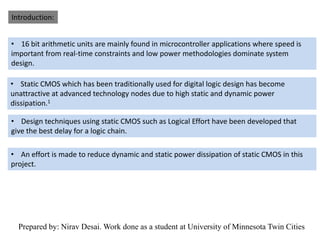
- 1. Introduction: • 16 bit arithmetic units are mainly found in microcontroller applications where speed is important from real-time constraints and low power methodologies dominate system design. • Static CMOS which has been traditionally used for digital logic design has become unattractive at advanced technology nodes due to high static and dynamic power dissipation.1 • Design techniques using static CMOS such as Logical Effort have been developed that give the best delay for a logic chain. • An effort is made to reduce dynamic and static power dissipation of static CMOS in this project. Prepared by: Nirav Desai. Work done as a student at University of Minnesota Twin Cities
- 2. Brent Kung Adder Transistor Level Design Inverter Design Optimization V DD 110 100 V in V out CL TD*Iavg 90 80 • • • • 70 60 50 40 120 140 160 180 200 220 240 260 280 300 NMOS Width = 90nm PMOS / NMOS Length = 50nM Vdd = 1.1V Current Averaged Over One Period of 2 ns • Optimal PMOS Width = 165nM • βinverter = 165/90 = 1.834 • Sizing for NAND, NOR and XOR Changed appropriately PMOS Width (nM) Work done as a student at the University of Minnesota, Twin Cities by Nirav Desai desai.nirav.12.09@gmail.com
- 3. Design Equations for Brent Kung Adder Gi = Ai AND Bi … (1) Pi = Ai XOR Bi … (2) Gi1=Gi + Pi AND Gi-1 … (3) Pi1=Pi AND Pi-1 … (4) Brent Kung Adder Gate Level Diagram 1. Input Block with Pre Computation 1.097X 3.883X Input Adder Chain 1 1X Gi + Pi*Gi-1 1.224X Input Adder Chain 2 1.562X 1X 10.1683X Input Adder Chain 3 1.553X 36X Output Buffers to drive Capacitive Loads 3.043X 1X 1.108X Input Adder Chain 4 Pi*Pi-1 1.23X 2.943X 1X 1.274X 10.8506X 40X 1.034X Output Buffers to drive Capacitive Loads Work done as a student at the University of Minnesota, Twin Cities by Nirav Desai desai.nirav.12.09@gmail.com
- 4. Design Equations for Brent Kung Adder Gi = Ai AND Bi … (1) Pi = Ai XOR Bi … (2) Gi1=Gi + Pi AND Gi-1 … (3) Pi1=Pi AND Pi-1 … (4) Brent Kung Adder Gate Level Diagram 2. Intermediate Dot Product Blocks Intermediate Adder Chain 1 Gi + Pi*Gi-1 1X Intermediate Adder Chain 2 6X 16X 1.72X 1X 1X 4X 1X 16X Pi*Pi-1 Output Buffers to drive Capacitive Loads Work done as a student at the University of Minnesota, Twin Cities by Nirav Desai desai.nirav.12.09@gmail.com
- 5. Brent Kung Adder Gate Level Diagram 3. Output Block for Post Computation Pi Design Equations for Brent Kung Adder Gi = Ai AND Bi … (1) Pi = Ai XOR Bi … (2) Gi1=Gi + Pi AND Gi-1 … (3) Pi1=Pi AND Pi-1 … (4) Si 1.182X 1.117X Ci-1 Output Buffers to drive Capacitive Loads Work done as a student at the University of Minnesota, Twin Cities by Nirav Desai desai.nirav.12.09@gmail.com
- 6. Work done as a student at the University of Minnesota, Twin Cities by Nirav Desai desai.nirav.12.09@gmail.com
- 7. Brent Kung Adder Transistor Level Design 1. Input Block with Pre Computation Input Adder Block Chain 1 Logical Effort Design for Signal Chains labeled in previous slide #2 Gi = logical effort Fi = fan out Si = sizing Bi = Branching in Gate Number Gate Name g value f value b value S Value Stage G 1.000 2.000 3.000 4.000 5.000 Stage F Stage B Stage H Gate H BUFFER INVERTER NOR INVERTER NAND LOAD h 1.000 1.000 1.646 1.000 1.352 36.000 2.225 36.000 6.943 556.248 3.540 3.540 3.540 2.151 3.540 2.618648 2.893 2.400 1.000 1.000 1.000 1.000 1.000 1.224 1.097 3.883 10.16831 36.000 Input Adder Block Chain 2 Gate Number Gate Name g value f value b value S Value 1.000 2.000 3.000 BUFFER INVERTER XOR NAND 1.000 1.000 1.893 4.518 4.518 2.386 2.893 2.400 1.780 1.000 1.562 1.553 Stage G Stage F Stage B Stage H 4.000 LOAD 1.295 3.488 1.000 3.043 13.748 2.451 13.748 12.359 Gate H h 416.510 4.518 1.000 13.748 Input Adder Block Chain 3 Gate Number Gate Name g value f value b value S Value 1.000 2.000 3.000 BUFFER INVERTER NOR 1.000 1.000 1.646 3.558 3.558 2.162 2.893 2.400 1.000 1.000 1.230 1.108 Stage G Stage F Stage B Stage H LOAD 3.941 1.646 3.941 6.943 45.038 Gate H h 3.558 3.941 Input Adder Block Chain 4 Gate Number Gate Name g value f value b value S Value Stage G 1.000 2.000 3.000 4.000 5.000 Stage F Stage B Stage H Gate H BUFFER INVERTER XOR NAND INVERTER LOAD h 1.000 1.000 1.893 1.295 1.000 40.000 2.451 40.000 6.943 680.832 3.686 3.686 3.686 1.947 2.847 3.686447 2.893 2.400 1.000 1.000 1.000 1.000 1.000 1.274 1.034 2.943 10.85056 40.000 3.94084 Work done as a student at the University of Minnesota, Twin Cities by Nirav Desai desai.nirav.12.09@gmail.com
- 8. Brent Kung Adder Transistor Level Design 2. Intermediate Dot Product Blocks Intermediate Adder Block Chain 1 Gate Number Gate Name g value f value b value S Value 1.000 2.000 INVERTER NAND LOAD 1.000 1.352 1.000 2.848 2.107 2.848 1.000 1.000 1.000 1.000 2.107 6.000 Stage G 1.352 Stage F 6.000 Stage B 1.000 Stage H Gate H h 8.112 2.848 Intermediate Adder Block Chain 2 Gate Number Gate Name g value f value b value S Value 1.000 2.000 BUFFER NAND 1.000 1.352 2.775 2.053 2.000 1.000 1.000 1.026 Gi = logical effort Fi = fan out Si = sizing Bi = Branching in Stage G LOAD 2.848 1.352 Stage F 2.848 Stage B 2.000 Stage H Gate H h 7.701 2.775 Logical Effort Design for Signal Chains labeled in previous slide #2 Work done as a student at the University of Minnesota, Twin Cities by Nirav Desai desai.nirav.12.09@gmail.com
- 9. Brent Kung Adder Transistor Level Design XOR GATE Work done as a student at the University of Minnesota, Twin Cities by Nirav Desai desai.nirav.12.09@gmail.com
- 10. Brent Kung Adder Layout Input Block with Pre Computation Input Inverters for Bit 0 and Bit 1 XOR Output Buffers PEX waveforms show larger size may be needed NAND 10X Work done as a student at the University of Minnesota, Twin Cities by Nirav Desai desai.nirav.12.09@gmail.com
- 11. Brent Kung Adder Layout XOR 1.553X Work done as a student at the University of Minnesota, Twin Cities by Nirav Desai desai.nirav.12.09@gmail.com
- 12. Brent Kung Adder Layout Intermediate Dot Product Generator Output Buffers PEX Waveforms show larger Size may be necessary here Work done as a student at the University of Minnesota, Twin Cities by Nirav Desai desai.nirav.12.09@gmail.com
- 13. Brent Kung Adder Layout Output Stage with Buffers Work done as a student at the University of Minnesota, Twin Cities by Nirav Desai desai.nirav.12.09@gmail.com
- 14. Brent Kung Adder Layout Full Layout: 49.5um X 48.6um Work done as a student at the University of Minnesota, Twin Cities by Nirav Desai desai.nirav.12.09@gmail.com
- 15. Brent Kung Adder Worst Case Delay Input Pattern: A: FFFF B: 0000 -> 0001 Dotted Lines show Carry Bits 15 and 14 Carry Bit 15 Carry Bit 14 Work done as a student at the University of Minnesota, Twin Cities by Nirav Desai desai.nirav.12.09@gmail.com
- 16. Output waveforms after parasitic extraction from layout: Sum Bit 0 Work done as a student at the University of Minnesota, Twin Cities by Nirav Desai desai.nirav.12.09@gmail.com
- 17. Output waveforms after parasitic extraction from layout: Sum Bit 14 Work done as a student at the University of Minnesota, Twin Cities by Nirav Desai desai.nirav.12.09@gmail.com
- 18. Brent Kung Adder Simulated Performance Simulations with maximally sized 1 stage buffers as determined by Logical Effort Design of individual chains Voltage (V) Delay Max-C14 (nS) Power Max (mW) Power-Delay 1.1 0.359 6.73 2.41 0.9 0.503 2.95 1.483 0.7 0.937 0.924 0.865 Product (xE-12) Simulations with minimally sized 1 stage buffers Voltage (V) Delay Max-C14 (nS) Power Max (mW) Power-Delay 1.1 0.403 5.186 2.089 0.9 0.569 2.277 1.295 0.7 1.069 0.692 0.739 Product (xE-12) Without Parasitic Extraction and Interconnect Parasitics buffering doesn’t improve performance significantly. Work done as a student at the University of Minnesota, Twin Cities by Nirav Desai desai.nirav.12.09@gmail.com
- 19. Comparison with other similar works: Sr. No. Group Name Adder Type Technology Adder Delay Power Consumption Power Delay Product 1 [1] University of Waterloo Department of ECE 16 bit Kogge Stone FPGA 45nM 419ps 13.29mW 5.57E-12 2 This work 16 bit Brent Kung Adder NCSU 45nM Free PDK ASIC 359ps 6.73mW 2.41E-12 3 [4] University of Texas, Tyler Department of EE 16 bit Kogge Stone Spartan 3e 90nM 6.286ns -- -- 4 [2] VIT University, Vellore 16 bit Kogge Stone SPARTAN 3e 90nM 599ns 46.16uW 2.76E-11 5 [2] VIT University, Vellore 16 bit Brent Kung Adder Spartan 3e 90nM 762ns 32.465uW 2.47E-11 8 [5] University of Wisconsin, Madison 16 bit Ripple Carry Adder LSI Logic 110nM ASIC 2.59ns -- -- 9 [5] University of Wisconsin, Madison 16 bit Carry Lookahead Adder LSI Logic 110nM ASIC 1.09ns -- -- 6 [3] Concordia University Department of ECS 16 bit Brent Kung Adder Virtex 2 130nM 26.94ns 1.15W 3.10E-08 7 [3] Concordia University Department of ECS 16 bit Kogge Stone Virtex 2 130nM 25.59ns 1.5546W 3.97E-08 Column1 Work done as a student at the University of Minnesota, Twin Cities by Nirav Desai desai.nirav.12.09@gmail.com
- 20. References: Comparison with other similar works: Work done as a student at the University of Minnesota, Twin Cities by Nirav Desai desai.nirav.12.09@gmail.com
- 21. References: 1. K. Nose and T. Sakurai, “Optimization of VDD and VTH for low power high speed applications,” in ACM/IEEE Design Automation Conference (DAC) Digest of Technical Papers, 2000, pp. 469-474 From: Sub-threshold Design for Ultra Low-Power Systems Alice Wang, Benton Highsmith Calhoun, Anantha P. Chandrakasan 2. Logical Effort by Ivan Sutherland, Bob Sproull and David Harris (Book) 3. Digital Integrated Circuits by Jan Rabaey, Anantha Chandrakasan, Borivoje Nikolic (Book) 4. A high-density sub-threshold SRAM with data-independent bit line leakage and virtualground replica scheme Tae-Hyoung Kim, Jason Liu, John Keane, Chris Kim, University of Minnesota ISSCC 2007 5. The Design of CMOS Radio-Frequency Integrated Circuits by Thomas Lee (Book) Work done as a student at the University of Minnesota, Twin Cities by Nirav Desai desai.nirav.12.09@gmail.com