Asian Journal of Applied Science and Technology (AJAST)
Volume 1, Issue 2, Pages 26-30, March 2017
© 2017 AJAST All rights reserved. www.ajast.net
Page | 26
Design of Low Power Energy Efficient Carry Select Adder Using CMOS
Technology
A.Neethumol1
and S.Gnanamurugan2
1
PG Student, Department of ECE, Vivekanandha College of Engineering for Women, India. Email: 05neethuajayan@gmail.com
2
Assistant Professor, Department of ECE, Vivekanandha College of Engineering for Women, India. Email: sgmvcew@gmail.com
Article Received: 19 February 2017 Article Accepted: 28 February 2017 Article Published: 01 March 2017
1. INTRODUCTION
Adders are the main building block in arithmetic and logic
units (ALUs). Increasing the speed and reducing the
power/energy consumption of adders will strongly influence
the speed and power consumption of processors. Nowadays
many works are there for optimizing the speed and power
consumption of adders. Definitely, it is highly desirable to
obtain higher speeds at low-power/energy consumptions. It
became a challenge for the designers of general purpose
processors.
One of the efficient techniques to lower the power
consumption of digital circuits is to reduce the supply voltage
due to quadratic dependence of the switching energy on the
voltage. Moreover, the main leakage component in OFF
devices is the subthreshold current, which has an exponential
dependence on the supply voltage level through the
drain-induced barrier lowering effect. Based on the amount of
the supply voltage reduction, the operation of ON devices
may occupy in the super threshold, near-threshold, or
subthreshold regions. Working in the super threshold region
provides lower delay and higher switching and leakage
powers compared with the near/subthreshold regions. The
logic gate delay and leakage power exhibit exponential
dependences on the supply and threshold voltages in the
subthreshold region. In addition, these voltages are
(potentially) subject to process and environmental variations
in the nanoscale technologies. These variations increase the
uncertainties in aforesaid performance parameters. For the
circuits operating in the subthreshold region, the small
subthreshold current causes a large delay.
Currently, the near-threshold region has been considered as a
region that provides a more desirable tradeoff point between
delay and power dissipation compared with that of the
subthreshold one, because it results in lower delay compared
with the subthreshold region and significantly lowers
switching and leakage powers compared with the super
threshold region. Moreover, near-threshold operation, which
uses supply voltage levels near the threshold voltage of
transistors, which considerably less from the process and
environmental variations by comparing with the subthreshold
region. The power and performance depending on the supply
voltage has been the motivation for designing the circuits with
dynamic voltage and frequency scaling. In these circuits, the
energy consumption can be reduced by, changing the voltage
(and frequency) of the circuit based on the workload
requirement. For these systems, the circuit must be able to
operating under a wide range of the supply voltage levels.
Carry select adder architecture consists of independent
generation of sum and carry. That is carry in equal to zero and
carry in equal to one are executed
2. CSA STRUCTURE
The carry-select adder mostly consists of two ripple carry
adders and a multiplexer. Adding two n-bit numbers through a
carry-select adder is done with two adders (therefore two
ripple carry adders) in order to perform the calculation twice,
one time with the hypothesis of the carry being zero and the
other with a hypothesis of one. Later the two results are
calculated, the correct sum, as well as the correct carry out, is
then selected with the multiplexer when the correct carry in is
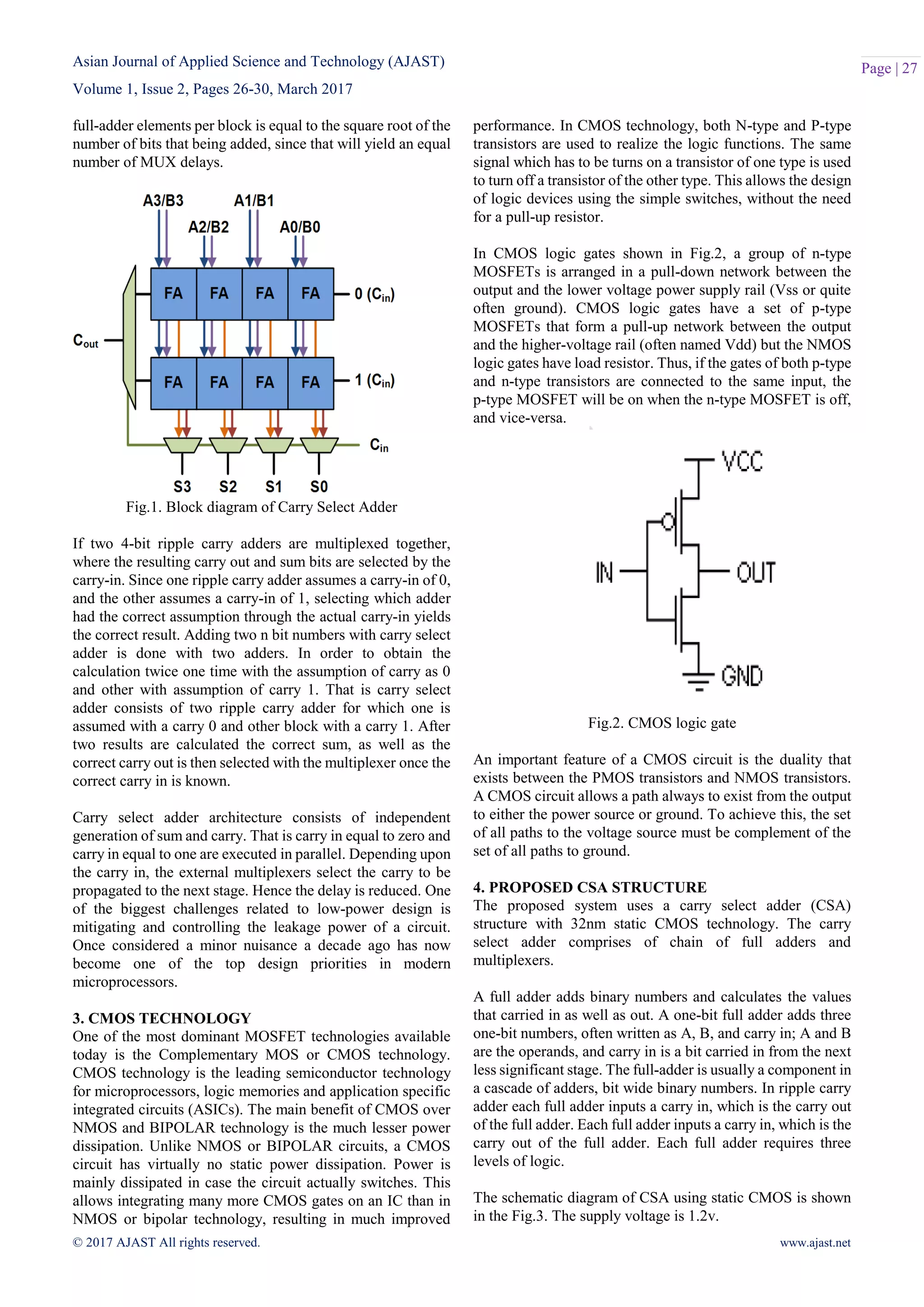
known. The basic building block of a carry-select adder [1],
where the block size is 4 is shown in the Fig.1.
The block size should have a delay when variable inputs are
given to the circuit. In addition, inputs A and B to the carry
out, equal to that of the multiplexer chain which leading into
it, so that the carry out is calculated just in time. The delay is
obtained from uniform sizing, where the ideal number of
ABSTRACT
This paper presents a recursive designing approach for high energy efficient carry select adder (CSA). Nowadays, the portable equipment’s like
mobile phones and laptops have higher demands in the market. So, the designers must focus greater attention while designing such devices. Which
means that have the devices must have lesser power consumption, low cost and have a better performance. The customers mainly focus on the
equipment’s which have lesser power consumption, low cost and better performance. As we all know that the adders are the basic building block of
microprocessors. The performance of the adders greatly influences the performance of those processors. The carry select adder is most suitable
among other adders which have fast addition operation at low cost. The carry select adder (CSA) consists of chain full adders (FAs) and multiplexers.
Here a carry select adder is designed with four FAs and four multiplexers. The proposed structure is assessed by the power consumption of the carry
select adder using a 32-nm static CMOS technology for a wide range of supply voltages. The simulation results are obtained using Tanner EDA which
reveals that the carry select adder has low power consumption.
Keywords: CSA, FAs and CMOS technology.
Asian Journal of Applied Science and Technology (AJAST)
Volume 1, Issue 2, Pages 26-30, March 2017
© 2017 AJAST All rights reserved. www.ajast.net
Page | 27
full-adder elements per block is equal to the square root of the
number of bits that being added, since that will yield an equal
number of MUX delays.
Fig.1. Block diagram of Carry Select Adder
If two 4-bit ripple carry adders are multiplexed together,
where the resulting carry out and sum bits are selected by the
carry-in. Since one ripple carry adder assumes a carry-in of 0,
and the other assumes a carry-in of 1, selecting which adder
had the correct assumption through the actual carry-in yields
the correct result. Adding two n bit numbers with carry select
adder is done with two adders. In order to obtain the
calculation twice one time with the assumption of carry as 0
and other with assumption of carry 1. That is carry select
adder consists of two ripple carry adder for which one is
assumed with a carry 0 and other block with a carry 1. After
two results are calculated the correct sum, as well as the
correct carry out is then selected with the multiplexer once the
correct carry in is known.
Carry select adder architecture consists of independent
generation of sum and carry. That is carry in equal to zero and
carry in equal to one are executed in parallel. Depending upon
the carry in, the external multiplexers select the carry to be
propagated to the next stage. Hence the delay is reduced. One
of the biggest challenges related to low-power design is
mitigating and controlling the leakage power of a circuit.
Once considered a minor nuisance a decade ago has now
become one of the top design priorities in modern
microprocessors.
3. CMOS TECHNOLOGY
One of the most dominant MOSFET technologies available
today is the Complementary MOS or CMOS technology.
CMOS technology is the leading semiconductor technology
for microprocessors, logic memories and application specific
integrated circuits (ASICs). The main benefit of CMOS over
NMOS and BIPOLAR technology is the much lesser power
dissipation. Unlike NMOS or BIPOLAR circuits, a CMOS
circuit has virtually no static power dissipation. Power is
mainly dissipated in case the circuit actually switches. This
allows integrating many more CMOS gates on an IC than in
NMOS or bipolar technology, resulting in much improved
performance. In CMOS technology, both N-type and P-type
transistors are used to realize the logic functions. The same
signal which has to be turns on a transistor of one type is used
to turn off a transistor of the other type. This allows the design
of logic devices using the simple switches, without the need
for a pull-up resistor.
In CMOS logic gates shown in Fig.2, a group of n-type
MOSFETs is arranged in a pull-down network between the
output and the lower voltage power supply rail (Vss or quite
often ground). CMOS logic gates have a set of p-type
MOSFETs that form a pull-up network between the output
and the higher-voltage rail (often named Vdd) but the NMOS
logic gates have load resistor. Thus, if the gates of both p-type
and n-type transistors are connected to the same input, the
p-type MOSFET will be on when the n-type MOSFET is off,
and vice-versa.
Fig.2. CMOS logic gate
An important feature of a CMOS circuit is the duality that
exists between the PMOS transistors and NMOS transistors.
A CMOS circuit allows a path always to exist from the output
to either the power source or ground. To achieve this, the set
of all paths to the voltage source must be complement of the
set of all paths to ground.
4. PROPOSED CSA STRUCTURE
The proposed system uses a carry select adder (CSA)
structure with 32nm static CMOS technology. The carry
select adder comprises of chain of full adders and
multiplexers.
A full adder adds binary numbers and calculates the values
that carried in as well as out. A one-bit full adder adds three
one-bit numbers, often written as A, B, and carry in; A and B
are the operands, and carry in is a bit carried in from the next
less significant stage. The full-adder is usually a component in
a cascade of adders, bit wide binary numbers. In ripple carry
adder each full adder inputs a carry in, which is the carry out
of the full adder. Each full adder inputs a carry in, which is the
carry out of the full adder. Each full adder requires three
levels of logic.
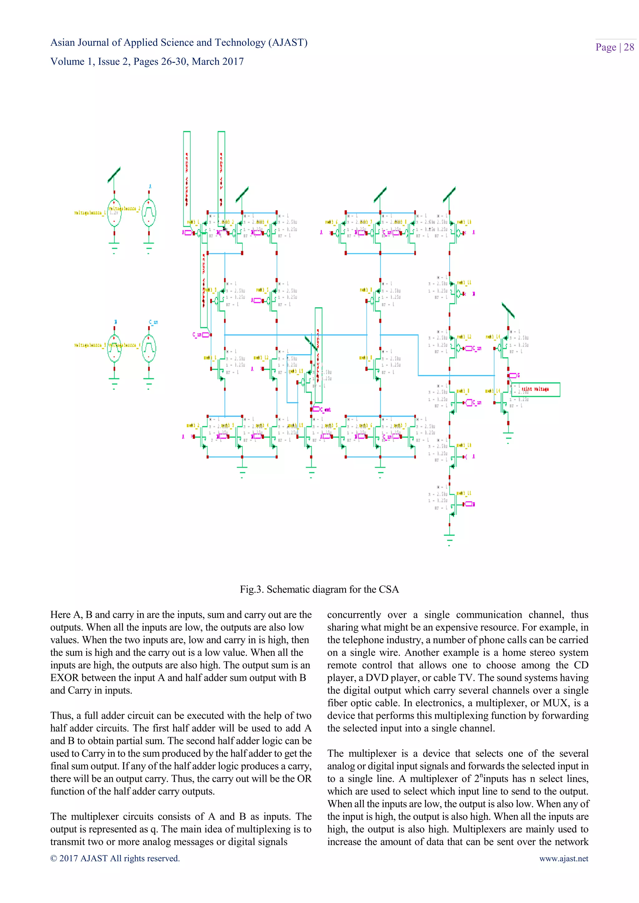
The schematic diagram of CSA using static CMOS is shown
in the Fig.3. The supply voltage is 1.2v.
Asian Journal of Applied Science and Technology (AJAST)
Volume 1, Issue 2, Pages 26-30, March 2017
© 2017 AJAST All rights reserved. www.ajast.net
Page | 28
Fig.3. Schematic diagram for the CSA
Here A, B and carry in are the inputs, sum and carry out are the
outputs. When all the inputs are low, the outputs are also low
values. When the two inputs are, low and carry in is high, then
the sum is high and the carry out is a low value. When all the
inputs are high, the outputs are also high. The output sum is an
EXOR between the input A and half adder sum output with B
and Carry in inputs.
Thus, a full adder circuit can be executed with the help of two
half adder circuits. The first half adder will be used to add A
and B to obtain partial sum. The second half adder logic can be
used to Carry in to the sum produced by the half adder to get the
final sum output. If any of the half adder logic produces a carry,
there will be an output carry. Thus, the carry out will be the OR
function of the half adder carry outputs.
The multiplexer circuits consists of A and B as inputs. The
output is represented as q. The main idea of multiplexing is to
transmit two or more analog messages or digital signals
concurrently over a single communication channel, thus
sharing what might be an expensive resource. For example, in
the telephone industry, a number of phone calls can be carried
on a single wire. Another example is a home stereo system
remote control that allows one to choose among the CD
player, a DVD player, or cable TV. The sound systems having
the digital output which carry several channels over a single
fiber optic cable. In electronics, a multiplexer, or MUX, is a
device that performs this multiplexing function by forwarding
the selected input into a single channel.
The multiplexer is a device that selects one of the several
analog or digital input signals and forwards the selected input in
to a single line. A multiplexer of 2n
inputs has n select lines,
which are used to select which input line to send to the output.
When all the inputs are low, the output is also low. When any of
the input is high, the output is also high. When all the inputs are
high, the output is also high. Multiplexers are mainly used to
increase the amount of data that can be sent over the network
Asian Journal of Applied Science and Technology (AJAST)
Volume 1, Issue 2, Pages 26-30, March 2017
© 2017 AJAST All rights reserved. www.ajast.net
Page | 29
within a certain amount of time and bandwidth. In this MUX
one selection line (S) is used to select one of 21
=2 input lines,
D0 and D1, whose data is to be sent to the output (q).
5. MEASUREMENT RESULTS
The simulation results of the proposed system are obtained
using Tanner EDA. The simulated waveform of the carry
select adder is shown in the Fig.4s below.
Here A, B and Carry in are the inputs. Sum and Carry out are the
output. From the waveform, it is clear that the when all the
inputs are a low value, the outputs are also a low value.
Similarly, when all the inputs are high, the outputs are also high.
Thus, a full adder circuit can be executed with the help of two
half adder circuits. The first half adder will be used to add A and
B to obtain partial sum. The main idea of multiplexing is to
transmit two or more analog messages or digital signals
concurrently over a single communication channel, thus
sharing what might be an expensive resource.
The simulated waveform of 2:1 multiplexer is shown in the
Fig.6. A multiplexer of 2n
inputs has n selection lines, which are
used to select which of the input line is send to the output. Here
D0 and D1 are inputs, S is the selection line. The output is
represented by q. Based on the select line the inputs are selected.
When all the inputs are low, the output is also low. When any of
the input is high, the output is also high. The multiplexer is a
device that selects one of the several analog or digital input
signals and forwards the selected input in to a single line. In this
MUX one selection line (S) is used to select one of 21
=2 input
lines, D0 and D1, whose data is to be sent to the output (q).
Fig.4. Simulated waveform of CSA
The power/energy consumption of the carry select adder is
obtained using Tanner EDA tool.
From the analysis, the average power consumed by the carry
select adder is 2.7µw. The maximum power obtained is
13.1mw and the minimum power is 2.62nw. Thus, the
simulation results reveal that the carry select adder has low
power consumption. In this MUX one selection line (S) is used
to select one of 21
=2 input lines, D0 and D1, whose data is to
be sent to the output (q).
6. CONCLUSION
In future, the concatenation and incrementation schemes are
applicable to design the carry select adder structure using static
CMOS technology. The concatenation and incrementation
methods are used to improve the efficiency of the carry select
adder and here by reducing the delay and the power
consumption of the adder. The carry select adder consists of full
adders and multiplexers. Here a simple carry select adder is
designed with four block of FAs and four 2:1 multiplexers
using the Tanner EDA tool. The proposed CSA system is
simulated in 32nm CMOS technology at supply voltage of
1.2V. The power consumption of the carry select adder is
2.7µW.
REFERENCES
[1] Neethumol.A, Gnanamurugan.S (2016), “Designing of
High performance carry select adder using CMOS
technology”, IJCAT, vol.3, Issue.11.
[2] Milad Bahodari, Mehadi Kamal, Ali-Afzali-Kusha
(2016), “High speed and Energy Efficient Carry Skip adder
operating under a wide range of supply voltage levels”, IEEE
Trans. VLSI Syst., vol.24, Issue.2.
[3] Jain. S et al., (2012), “A 280mV to 1.2V wide operating
range IA-32 processor in 32nm CMOS”, IEEE Int. Solid State
Asian Journal of Applied Science and Technology (AJAST)
Volume 1, Issue 2, Pages 26-30, March 2017
© 2017 AJAST All rights reserved. www.ajast.net
Page | 30
Circuits Conf. Dig. Tech. Papers (ISSCC), vol.40, no.1,
pp.44-51.
[4] Su. Y.S, Wang. D.C, Chang. S.C and Marek Sadowska.
M, (2011), “Performance optimization using variable latency
design style”, IEEE Trans. Very Large Scale Integr. (VLSI)
Syst., vol. 19, no. 10, pp.1874-1883.
[5] Markovic. D,Wang. C.C, Alarcon. L.P, Liu. T.T, and
Rabaey. J.B (2010), “Ultra low power design in near threshold
region”, Proc. IEEE, vol.98, no.2, pp.237-252.
[6] Chen.Y et al., (2010), “Variable latency Adder
(VL-Adder) designs for low power and NBTI Tolerance”,
IEEE Trans. (VLSI) Syst., vol. 18, no.11, pp.1621-1624.
[7] Ghosh.S, Mohaputra.D, Karakonstantis.G and Roy.K,
(2010), “Voltage Scalable High-Speed Robust Hybrid
Arithmetic Units Using Adaptive Clocking”, IEEE Trans.
Very Large Scale Integr. (VLSI) Syst., vol.18, no.9,
pp.1301-1309.
[8] Zlatanovici. R, Kao. S and Nikolic. B, (2009),
“Energy–Delay Optimization of 64-Bit Carry-Look ahead
Adders With a 240 ps 90 nm CMOS Design Example”, IEEE
J. Solid State Circuits, vol. 44, no. 2, pp.569-583.
[9] He.Y and Chang. C.H, (2008), “A Power-Delay Efficient
Hybrid Carry-Look ahead/ Carry-Select Based Redundant
Binary to Two’s Complement Converter”, IEEE Trans.Circuits
Syst.I Reg. Papers, vol. 55, no.1, pp.336-346.
[10] Okalobdzijia. V.G, Zeydel. B.R, Dao. H.Q, Mathew. S,
Krishnamurthy. R, (2005), “Comparison of High-Performance
VLSI Adders in the Energy-Delay Space”, IEEE Trans. VLSI
Syst., vol.13, no.6, pp.754-758.
[11] Mathew. S.K, Anders. M.A, Blochel. B, Nguygen. T,
Krishnamurthy. R.K and Borkar.S, (2005), “A 4GHz 300-mW
64-bit integer execution ALU with dual supply voltages in
90nm CMOS”, IEEE J. Solid State Circuits, vol. 40, no. 1,
pp.44-51.

Design of Low Power Energy Efficient Carry Select Adder Using CMOS Technology

  • 1.
    Asian Journal ofApplied Science and Technology (AJAST) Volume 1, Issue 2, Pages 26-30, March 2017 © 2017 AJAST All rights reserved. www.ajast.net Page | 26 Design of Low Power Energy Efficient Carry Select Adder Using CMOS Technology A.Neethumol1 and S.Gnanamurugan2 1 PG Student, Department of ECE, Vivekanandha College of Engineering for Women, India. Email: 05neethuajayan@gmail.com 2 Assistant Professor, Department of ECE, Vivekanandha College of Engineering for Women, India. Email: sgmvcew@gmail.com Article Received: 19 February 2017 Article Accepted: 28 February 2017 Article Published: 01 March 2017 1. INTRODUCTION Adders are the main building block in arithmetic and logic units (ALUs). Increasing the speed and reducing the power/energy consumption of adders will strongly influence the speed and power consumption of processors. Nowadays many works are there for optimizing the speed and power consumption of adders. Definitely, it is highly desirable to obtain higher speeds at low-power/energy consumptions. It became a challenge for the designers of general purpose processors. One of the efficient techniques to lower the power consumption of digital circuits is to reduce the supply voltage due to quadratic dependence of the switching energy on the voltage. Moreover, the main leakage component in OFF devices is the subthreshold current, which has an exponential dependence on the supply voltage level through the drain-induced barrier lowering effect. Based on the amount of the supply voltage reduction, the operation of ON devices may occupy in the super threshold, near-threshold, or subthreshold regions. Working in the super threshold region provides lower delay and higher switching and leakage powers compared with the near/subthreshold regions. The logic gate delay and leakage power exhibit exponential dependences on the supply and threshold voltages in the subthreshold region. In addition, these voltages are (potentially) subject to process and environmental variations in the nanoscale technologies. These variations increase the uncertainties in aforesaid performance parameters. For the circuits operating in the subthreshold region, the small subthreshold current causes a large delay. Currently, the near-threshold region has been considered as a region that provides a more desirable tradeoff point between delay and power dissipation compared with that of the subthreshold one, because it results in lower delay compared with the subthreshold region and significantly lowers switching and leakage powers compared with the super threshold region. Moreover, near-threshold operation, which uses supply voltage levels near the threshold voltage of transistors, which considerably less from the process and environmental variations by comparing with the subthreshold region. The power and performance depending on the supply voltage has been the motivation for designing the circuits with dynamic voltage and frequency scaling. In these circuits, the energy consumption can be reduced by, changing the voltage (and frequency) of the circuit based on the workload requirement. For these systems, the circuit must be able to operating under a wide range of the supply voltage levels. Carry select adder architecture consists of independent generation of sum and carry. That is carry in equal to zero and carry in equal to one are executed 2. CSA STRUCTURE The carry-select adder mostly consists of two ripple carry adders and a multiplexer. Adding two n-bit numbers through a carry-select adder is done with two adders (therefore two ripple carry adders) in order to perform the calculation twice, one time with the hypothesis of the carry being zero and the other with a hypothesis of one. Later the two results are calculated, the correct sum, as well as the correct carry out, is then selected with the multiplexer when the correct carry in is known. The basic building block of a carry-select adder [1], where the block size is 4 is shown in the Fig.1. The block size should have a delay when variable inputs are given to the circuit. In addition, inputs A and B to the carry out, equal to that of the multiplexer chain which leading into it, so that the carry out is calculated just in time. The delay is obtained from uniform sizing, where the ideal number of ABSTRACT This paper presents a recursive designing approach for high energy efficient carry select adder (CSA). Nowadays, the portable equipment’s like mobile phones and laptops have higher demands in the market. So, the designers must focus greater attention while designing such devices. Which means that have the devices must have lesser power consumption, low cost and have a better performance. The customers mainly focus on the equipment’s which have lesser power consumption, low cost and better performance. As we all know that the adders are the basic building block of microprocessors. The performance of the adders greatly influences the performance of those processors. The carry select adder is most suitable among other adders which have fast addition operation at low cost. The carry select adder (CSA) consists of chain full adders (FAs) and multiplexers. Here a carry select adder is designed with four FAs and four multiplexers. The proposed structure is assessed by the power consumption of the carry select adder using a 32-nm static CMOS technology for a wide range of supply voltages. The simulation results are obtained using Tanner EDA which reveals that the carry select adder has low power consumption. Keywords: CSA, FAs and CMOS technology.
  • 2.
    Asian Journal ofApplied Science and Technology (AJAST) Volume 1, Issue 2, Pages 26-30, March 2017 © 2017 AJAST All rights reserved. www.ajast.net Page | 27 full-adder elements per block is equal to the square root of the number of bits that being added, since that will yield an equal number of MUX delays. Fig.1. Block diagram of Carry Select Adder If two 4-bit ripple carry adders are multiplexed together, where the resulting carry out and sum bits are selected by the carry-in. Since one ripple carry adder assumes a carry-in of 0, and the other assumes a carry-in of 1, selecting which adder had the correct assumption through the actual carry-in yields the correct result. Adding two n bit numbers with carry select adder is done with two adders. In order to obtain the calculation twice one time with the assumption of carry as 0 and other with assumption of carry 1. That is carry select adder consists of two ripple carry adder for which one is assumed with a carry 0 and other block with a carry 1. After two results are calculated the correct sum, as well as the correct carry out is then selected with the multiplexer once the correct carry in is known. Carry select adder architecture consists of independent generation of sum and carry. That is carry in equal to zero and carry in equal to one are executed in parallel. Depending upon the carry in, the external multiplexers select the carry to be propagated to the next stage. Hence the delay is reduced. One of the biggest challenges related to low-power design is mitigating and controlling the leakage power of a circuit. Once considered a minor nuisance a decade ago has now become one of the top design priorities in modern microprocessors. 3. CMOS TECHNOLOGY One of the most dominant MOSFET technologies available today is the Complementary MOS or CMOS technology. CMOS technology is the leading semiconductor technology for microprocessors, logic memories and application specific integrated circuits (ASICs). The main benefit of CMOS over NMOS and BIPOLAR technology is the much lesser power dissipation. Unlike NMOS or BIPOLAR circuits, a CMOS circuit has virtually no static power dissipation. Power is mainly dissipated in case the circuit actually switches. This allows integrating many more CMOS gates on an IC than in NMOS or bipolar technology, resulting in much improved performance. In CMOS technology, both N-type and P-type transistors are used to realize the logic functions. The same signal which has to be turns on a transistor of one type is used to turn off a transistor of the other type. This allows the design of logic devices using the simple switches, without the need for a pull-up resistor. In CMOS logic gates shown in Fig.2, a group of n-type MOSFETs is arranged in a pull-down network between the output and the lower voltage power supply rail (Vss or quite often ground). CMOS logic gates have a set of p-type MOSFETs that form a pull-up network between the output and the higher-voltage rail (often named Vdd) but the NMOS logic gates have load resistor. Thus, if the gates of both p-type and n-type transistors are connected to the same input, the p-type MOSFET will be on when the n-type MOSFET is off, and vice-versa. Fig.2. CMOS logic gate An important feature of a CMOS circuit is the duality that exists between the PMOS transistors and NMOS transistors. A CMOS circuit allows a path always to exist from the output to either the power source or ground. To achieve this, the set of all paths to the voltage source must be complement of the set of all paths to ground. 4. PROPOSED CSA STRUCTURE The proposed system uses a carry select adder (CSA) structure with 32nm static CMOS technology. The carry select adder comprises of chain of full adders and multiplexers. A full adder adds binary numbers and calculates the values that carried in as well as out. A one-bit full adder adds three one-bit numbers, often written as A, B, and carry in; A and B are the operands, and carry in is a bit carried in from the next less significant stage. The full-adder is usually a component in a cascade of adders, bit wide binary numbers. In ripple carry adder each full adder inputs a carry in, which is the carry out of the full adder. Each full adder inputs a carry in, which is the carry out of the full adder. Each full adder requires three levels of logic. The schematic diagram of CSA using static CMOS is shown in the Fig.3. The supply voltage is 1.2v.
  • 3.
    Asian Journal ofApplied Science and Technology (AJAST) Volume 1, Issue 2, Pages 26-30, March 2017 © 2017 AJAST All rights reserved. www.ajast.net Page | 28 Fig.3. Schematic diagram for the CSA Here A, B and carry in are the inputs, sum and carry out are the outputs. When all the inputs are low, the outputs are also low values. When the two inputs are, low and carry in is high, then the sum is high and the carry out is a low value. When all the inputs are high, the outputs are also high. The output sum is an EXOR between the input A and half adder sum output with B and Carry in inputs. Thus, a full adder circuit can be executed with the help of two half adder circuits. The first half adder will be used to add A and B to obtain partial sum. The second half adder logic can be used to Carry in to the sum produced by the half adder to get the final sum output. If any of the half adder logic produces a carry, there will be an output carry. Thus, the carry out will be the OR function of the half adder carry outputs. The multiplexer circuits consists of A and B as inputs. The output is represented as q. The main idea of multiplexing is to transmit two or more analog messages or digital signals concurrently over a single communication channel, thus sharing what might be an expensive resource. For example, in the telephone industry, a number of phone calls can be carried on a single wire. Another example is a home stereo system remote control that allows one to choose among the CD player, a DVD player, or cable TV. The sound systems having the digital output which carry several channels over a single fiber optic cable. In electronics, a multiplexer, or MUX, is a device that performs this multiplexing function by forwarding the selected input into a single channel. The multiplexer is a device that selects one of the several analog or digital input signals and forwards the selected input in to a single line. A multiplexer of 2n inputs has n select lines, which are used to select which input line to send to the output. When all the inputs are low, the output is also low. When any of the input is high, the output is also high. When all the inputs are high, the output is also high. Multiplexers are mainly used to increase the amount of data that can be sent over the network
  • 4.
    Asian Journal ofApplied Science and Technology (AJAST) Volume 1, Issue 2, Pages 26-30, March 2017 © 2017 AJAST All rights reserved. www.ajast.net Page | 29 within a certain amount of time and bandwidth. In this MUX one selection line (S) is used to select one of 21 =2 input lines, D0 and D1, whose data is to be sent to the output (q). 5. MEASUREMENT RESULTS The simulation results of the proposed system are obtained using Tanner EDA. The simulated waveform of the carry select adder is shown in the Fig.4s below. Here A, B and Carry in are the inputs. Sum and Carry out are the output. From the waveform, it is clear that the when all the inputs are a low value, the outputs are also a low value. Similarly, when all the inputs are high, the outputs are also high. Thus, a full adder circuit can be executed with the help of two half adder circuits. The first half adder will be used to add A and B to obtain partial sum. The main idea of multiplexing is to transmit two or more analog messages or digital signals concurrently over a single communication channel, thus sharing what might be an expensive resource. The simulated waveform of 2:1 multiplexer is shown in the Fig.6. A multiplexer of 2n inputs has n selection lines, which are used to select which of the input line is send to the output. Here D0 and D1 are inputs, S is the selection line. The output is represented by q. Based on the select line the inputs are selected. When all the inputs are low, the output is also low. When any of the input is high, the output is also high. The multiplexer is a device that selects one of the several analog or digital input signals and forwards the selected input in to a single line. In this MUX one selection line (S) is used to select one of 21 =2 input lines, D0 and D1, whose data is to be sent to the output (q). Fig.4. Simulated waveform of CSA The power/energy consumption of the carry select adder is obtained using Tanner EDA tool. From the analysis, the average power consumed by the carry select adder is 2.7µw. The maximum power obtained is 13.1mw and the minimum power is 2.62nw. Thus, the simulation results reveal that the carry select adder has low power consumption. In this MUX one selection line (S) is used to select one of 21 =2 input lines, D0 and D1, whose data is to be sent to the output (q). 6. CONCLUSION In future, the concatenation and incrementation schemes are applicable to design the carry select adder structure using static CMOS technology. The concatenation and incrementation methods are used to improve the efficiency of the carry select adder and here by reducing the delay and the power consumption of the adder. The carry select adder consists of full adders and multiplexers. Here a simple carry select adder is designed with four block of FAs and four 2:1 multiplexers using the Tanner EDA tool. The proposed CSA system is simulated in 32nm CMOS technology at supply voltage of 1.2V. The power consumption of the carry select adder is 2.7µW. REFERENCES [1] Neethumol.A, Gnanamurugan.S (2016), “Designing of High performance carry select adder using CMOS technology”, IJCAT, vol.3, Issue.11. [2] Milad Bahodari, Mehadi Kamal, Ali-Afzali-Kusha (2016), “High speed and Energy Efficient Carry Skip adder operating under a wide range of supply voltage levels”, IEEE Trans. VLSI Syst., vol.24, Issue.2. [3] Jain. S et al., (2012), “A 280mV to 1.2V wide operating range IA-32 processor in 32nm CMOS”, IEEE Int. Solid State
  • 5.
    Asian Journal ofApplied Science and Technology (AJAST) Volume 1, Issue 2, Pages 26-30, March 2017 © 2017 AJAST All rights reserved. www.ajast.net Page | 30 Circuits Conf. Dig. Tech. Papers (ISSCC), vol.40, no.1, pp.44-51. [4] Su. Y.S, Wang. D.C, Chang. S.C and Marek Sadowska. M, (2011), “Performance optimization using variable latency design style”, IEEE Trans. Very Large Scale Integr. (VLSI) Syst., vol. 19, no. 10, pp.1874-1883. [5] Markovic. D,Wang. C.C, Alarcon. L.P, Liu. T.T, and Rabaey. J.B (2010), “Ultra low power design in near threshold region”, Proc. IEEE, vol.98, no.2, pp.237-252. [6] Chen.Y et al., (2010), “Variable latency Adder (VL-Adder) designs for low power and NBTI Tolerance”, IEEE Trans. (VLSI) Syst., vol. 18, no.11, pp.1621-1624. [7] Ghosh.S, Mohaputra.D, Karakonstantis.G and Roy.K, (2010), “Voltage Scalable High-Speed Robust Hybrid Arithmetic Units Using Adaptive Clocking”, IEEE Trans. Very Large Scale Integr. (VLSI) Syst., vol.18, no.9, pp.1301-1309. [8] Zlatanovici. R, Kao. S and Nikolic. B, (2009), “Energy–Delay Optimization of 64-Bit Carry-Look ahead Adders With a 240 ps 90 nm CMOS Design Example”, IEEE J. Solid State Circuits, vol. 44, no. 2, pp.569-583. [9] He.Y and Chang. C.H, (2008), “A Power-Delay Efficient Hybrid Carry-Look ahead/ Carry-Select Based Redundant Binary to Two’s Complement Converter”, IEEE Trans.Circuits Syst.I Reg. Papers, vol. 55, no.1, pp.336-346. [10] Okalobdzijia. V.G, Zeydel. B.R, Dao. H.Q, Mathew. S, Krishnamurthy. R, (2005), “Comparison of High-Performance VLSI Adders in the Energy-Delay Space”, IEEE Trans. VLSI Syst., vol.13, no.6, pp.754-758. [11] Mathew. S.K, Anders. M.A, Blochel. B, Nguygen. T, Krishnamurthy. R.K and Borkar.S, (2005), “A 4GHz 300-mW 64-bit integer execution ALU with dual supply voltages in 90nm CMOS”, IEEE J. Solid State Circuits, vol. 40, no. 1, pp.44-51.