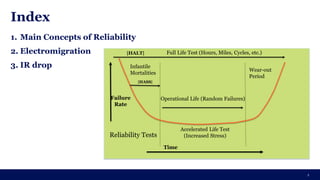
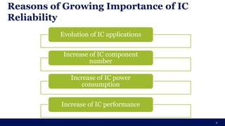
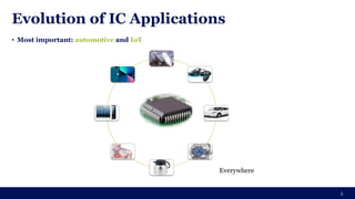
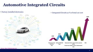
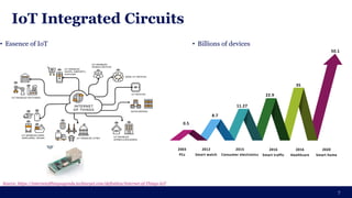
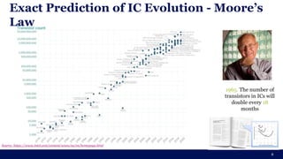
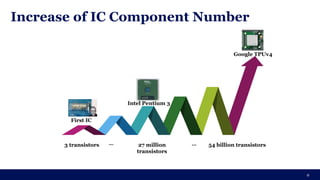
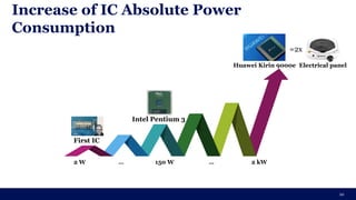
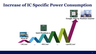
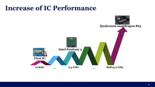
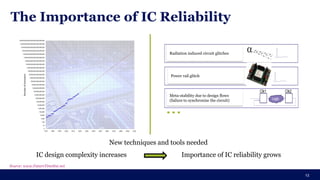
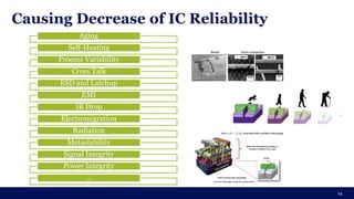
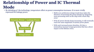
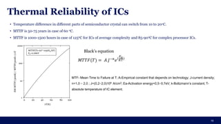
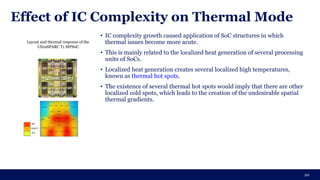
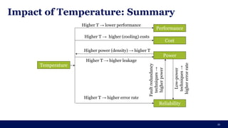
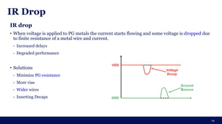
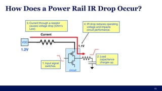
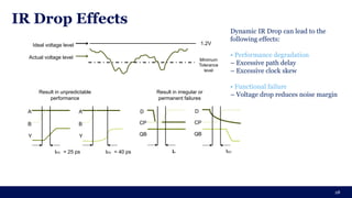
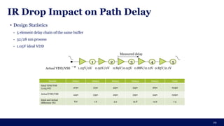
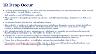
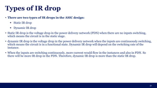
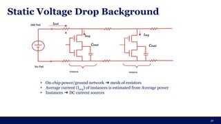
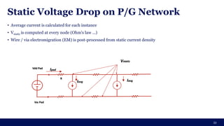
IC Reliability
EMIR
Ahmed Abdelazeem
Index
1. Main Concepts of Reliability
2. Electromigration
3. IR drop
1
Infantile
Mortalities
Failure
Rate
Operational Life (Random Failures)
Wear-out
Period
Time
Accelerated Life Test
(Increased Stress)
|HALT|
|HASS|
Full Life Test (Hours, Miles, Cycles, etc.)
Reliability Tests
• Physics
• Mathematics
• General knowledge on IC and its design
• General knowledge on IC fabrication technologies
• Basic knowledge of MOS and FinFET transistors
2
Prerequisites
Quality vs Reliability
• Quality
▪ A complete number of features and characteristics of a product that deliver specified needs.
• Reliability
▪ The capacity of a product to perform its required functions under specified conditions for a particular period. In
other words, reliability is the quality over time.
3
quality reliability
Source: https://www.techly.it/sedia-per-ufficio-easy-colore-blu.html
Reasons of Growing Importance of IC
Reliability
4
Evolution of IC applications
Increase of IC component
number
Increase of IC power
consumption
Increase of IC performance
Evolution of IC Applications
• Most important: automotive and IoT
5
Everywhere
Automotive Integrated Circuits
6
• Factory-installed electronics • Integrated Circuits as % of total car cost
Voice/Data
Communications
Cabin
Environment
Controls
DSRC
Entertainment
System
H ill-
H old Regenerative
Control
Braking
Antilock
The Pressure Braking
Monitoring
Parking
s ys tem
Security System
ActiveExhaust
Noise Suppression
ActiveSuspension
Battery
Management
Repair
Lane Correction
Electronic Toll
Collection
Digital
Turn
Signa
ls
Navigat
ion
Syste
m
Differen
tial
EV/HEV
Active
CabinNoise
Suppression
Interior
Lightering
Auto-
Dimming
Mirror
Event
Data
Recorder
Accident
Recorder
Instrument
Cluster
Driver
Alertness
Monit
oring
Windshield
WiperControl
Parental
Controls
Airbag
Deployment
Remote
Keyless
Entry
Blindspot
Direction
Lane
D eparture
Warning
Transmission
Control
ActiveYaw
Control
Electronic
stability
control
Seat
Position
control
AdaptiveFront
Lighting
AdaptiveCruise
Control
Automatic
Braking
Electric Power
Steering
Electronic Throttle
Control
Electronic Valve
Timing
Cylinder
D e-activation Active
Vibration
Control
Drive
Shaft
IdleStop/
Start OBDII
Engine
Control
Night
Vision
H ead-Up
Display
1980
Electronic fuel
injection
10%
Airbag ABS/ESP
22%
2000
Advanced driver assist Active-passive
safety
Powertrain Radar/ vision infotainment
35%
2010
2030
50%
Source: https://mfjenterprises.com
IoT Integrated Circuits
7
• Essence of IoT • Billions of devices
0.5
2003
PCs
8.7
22.9
50.1
2012
Smart watch
11.27
2015
Consumer electronics
2016
Smart traffic
2016
Healthcare
2020
Smart home
35
Source: https://internetofthingsagenda.techtarget.com/definition/Internet-of-Things-IoT
Exact Prediction of IC Evolution - Moore’s
Law
8
1965. The number of
transistors in ICs will
double every 18
months
Source: https://www.intel.com/content/www/us/en/homepage.html
Increase of IC Component Number
9
3 transistors 54 billion transistors
27 million
transistors
First IC
Intel Pentium 3
Google TPUv4
… …
Increase of IC Absolute Power
Consumption
10
2 W 2 kW
150 W
=2x
First IC
Intel Pentium 3
Huawei Kirin 9000e
… …
Electrical panel
Increase of IC Specific Power Consumption
11
∼1W/cm2 ∼300W/cm2
∼8W/cm2
∼
First IC
Intel Pentium 3
Google TPUv4
…
…
Nuclear reactor
Increase of IC Performance
12
10 kHz 8x8x5,2 GHz
2,3 GHz
∼
First IC
Intel Pentium 3
Qualcomm snapdragon 865
…
…
The Importance of IC Reliability
13
Radiation induced circuit glitches
Power rail glitch
Meta-stability due to design flows
(failure to synchronize the circuit)
IC design complexity increases Importance of IC reliability grows
New techniques and tools needed
Source: www.FutureTimeline.net
Causing Decrease of IC Reliability
14
Aging
Self-Heating
Process Variability
Cross Talk
ESD and Latchup
EMI
IR Drop
Electromigration
Radiation
Metastability
Signal Integrity
Power Integrity
…
Trends of Parameter Evolution With
Regards to IC Thermal Mode
15
• IC complexity increases, consideration and control of thermal mode during IC design becomes more important.
Year 2009 2012 2015 2018 2021 2024
Gate length (nm) 54 35 22 15,7 11,1 7,9
Average specific power consumption (W /
mm2)
0,45 0,6 0,75 0,9 1,05 1,2
In case of portable devices, maximum
temperature of p-n junction (0C)
105 105 105 105 105 105
Maximum operational temperature range (0C) -40...150 -40...150 -40...150 -40...150 -40...150 -40...150
In case of optimal flow of air, environment
temperature of IC body (0C)
45 45 45 45 45 45
IC Technology, Power Consumption and
Temperature Connection
16
• IC complexity increases and connections between different parameters also increases.
• For effective thermal management, it is necessary to take it into account during the whole design
flow.
Dynamic
Static
Technology, nm Temperature
Power
consumption
(W)
IC Design Flow and Thermal Analysis
17
IC
Design
Flow
Timing IR Drop
Rail EM
Thermal
Extraction
Power
• IC design success is largely determined by the availability of
such design environment that combines the interdependent
tasks of timing, power, leakage, thermal and signal analysis.
• Such analysis should be applied throughout the entire IC
design implementation process.
• By IC complexity growth (SoC, Multichip module, 3D IC)
and their use in portable devices, thermal analysis gets
particular importance
Relationship of Power and IC Thermal
Mode
18
• By shrinking of the technology, temperature effect on power consumption increases. It is more vividly
expressed for leakage power. • Multi-core architecture design trends have taken the
direction of increasing the power density by integrating
more processing units on the chip (with a fixed chip
area).
• If the IC power density keeps increasing, it will eventually
reach the same magnitude of nuclear power plants.
• With such increased power densities, ICs face a
tremendous increase in heat generation that has a direct
impact on the lifetime of ICs.
Dynamic Power Leakage Power
Total Power
Temperature
Thermal Reliability of ICs
19
• Temperature difference in different parts of semiconductor crystal can switch from 10 to 20oC.
• MTTF is 50-75 years in case of 60 oC.
• MTTF is 1000-1500 hours in case of 125oC for ICs of average complexity and 85-90oC for complex processor ICs.
Black’s equation
𝑀𝑇𝑇𝐹(𝑇) = 𝐴 𝐽−𝑛
𝑒(
𝐸𝑎
𝐾𝑇)
MTF- Mean Time to Failure at T; A-Empirical constant that depends on technology; J-current density;
n=1,0 ÷ 2,0 ; J=(0,2÷2,0)106 A/cm2; Ea-Activation energy=0,5÷0,7eV; k-Boltzmann’s constant; T-
absolute temperature of IC element.
1000
100
10
1
100
80
60
40
20
0
T(K)
MTTF(T)=AJ-2 exp(Ea/kT)
Ea=0.68eV
EM
MTTF
(300K)
/
MTTF(300K+)
T
Effect of IC Complexity on Thermal Mode
20
• IC complexity growth caused application of SoC structures in which
thermal issues become more acute.
• This is mainly related to the localized heat generation of several processing
units of SoCs.
• Localized heat generation creates several localized high temperatures,
known as thermal hot spots.
• The existence of several thermal hot spots would imply that there are other
localized cold spots, which leads to the creation of the undesirable spatial
thermal gradients.
Layout and thermal response of the
UltraSPARC T1 MPSoC
Impact of Temperature: Summary
21
Temperature
Performance
Power
Reliability
Cost
Higher T → lower performance
Higher T → higher (cooling) costs
Higher T → higher leakage
Higher T → higher error rate
Higher power (density) → higher T
Fault
redundancy
techniques
→
higher
power
Low-power
techniques
→
higher
error
rate
Gate-level Average Power Calculation
22
Leakage
Power
Internal
Power
Switching
Power
Average
Power
𝑃(𝑡𝑜𝑡𝑎𝑙) = 𝑃(𝐿𝑒𝑎𝑘𝑎𝑔𝑒) + ½ ∗ (𝐼𝑛𝑡𝑒𝑟𝑛𝑎𝑙 − 𝑒𝑛𝑒𝑟𝑔𝑦 ∗ 𝐹𝑟𝑒𝑞 ∗ 𝑇𝑅) + ½ ∗ 𝐶 ∗ 𝑉2
∗ 𝐹𝑟𝑒𝑞 ∗ 𝑇𝑅
Gate-level Average Power Calculation
23
IR Drop
24
IR drop
• When voltage is applied to PG metals the current starts flowing and some voltage is dropped due
to finite resistance of a metal wire and current.
- Increased delays
- Degraded performance
• Solutions
- Minimize PG resistance
- More vias
- Wider wires
- Inserting Decaps
How Does a Power Rail IR Drop Occur?
25
IR Drop (2)
• IR drop: Voltage drops caused
by current flowing from the
power source through the
resistive power network to the
on-chip devices is called IR drop.
• Ground bounce: Voltage
spikes caused by current flowing
from on-chip devices though the
resistive ground network to the
ground pins (or bumps)
• IR drop and ground bounce
combine to impact silicon
performance.
26
IR Drop Impacts on Setup and Hold Time
• In the case where the IR drop occurs within the signal path, the signal is slowed, potentially causing setup time
violations for this signal path
• In the case where IR drop occurs on a clock buffer, the clock signal beyond this buffer is slowed, potentially
causing hold time violations for all signals clocked by this clock branch.
27
IR Drop Effects
28
1.2V
Minimum
Tolerance
level
Ideal voltage level
Actual voltage level
A
B
Y
A
B
Y
D D
CP
QB
CP
QB
t = 25 ps
PD t = 40 ps
PD t
su tSU
Result in unpredictable
performance
Result in irregular or
permanent failures
Dynamic IR Drop can lead to the
following effects:
• Performance degradation
– Excessive path delay
– Excessive clock skew
• Functional failure
– Voltage drop reduces noise margin
IR Drop Impact on Path Delay
29
• Design Statistics
- 5 element delay chain of the same buffer
- 32/28 nm process
- 1.05V ideal VDD
1 2 3 4 5
Actual VDD/VSS 1.05V/0V 0.92V/0V 0.89V/0.05V 0.88V/0.12V 0.85V/0.1V
Measured delay
Results Delay1 Delay2 Delay3 Delay4 Delay5 Total
Ideal VDD/VSS
(1.05/0V) 40ps 51ps 53ps 54ps 56ps 254ps
Actual VDD/VSS 44ps 53ps 49ps 59ps 54ps 259ps
Ideal and Actual
difference (%)
8.6 1.6 3.2 15.8 14.9 7.3
IR Drop Occur
• The power supply (VDD and VSS) in a chip is uniformly distributed through the metal rails and stripes which is called
a Power Delivery Network (PDN) or power grid.
• Each metal layer used in PDN has finite resistivity.
• When current flows through the power delivery network, a part of the applied voltage will be dropped in PDN as per
Ohm’s law
• The amount of voltage drop will be V = I.R, called the IR drop.
• If the resistivity of metal wire is high or the amount of current following through the power net is high, A significant
amount of voltage may be dropped in the power delivery network which will cause a lesser amount of voltage
available to the standard cells than the actual amount of voltage applied.
• If V1 voltage is applied at the power port and current I is following in a particular net which has total resistance R,
then the voltage available (V2) to the other end for the standard cell will be
• Standard cells or macros sometimes do not get the minimum operating voltage which is required to operate them due
to IR drop in the power delivery network even the application of sufficient voltage in the power port.
• Voltage drop in the power delivery network before reaching the standard cells is called IR drop
• This drop may cause the poor performance of the chip due to the increase of delay of standard cells and may cause
the functional failure of the chip due to setup/hold timing violation.
30
Types of IR drop
• There are two types of IR drops in the ASIC design:
▪ Static IR drop
▪ Dynamic IR drop
• Static IR drop is the voltage drop in the power delivery network (PDN) when there are no inputs switching,
which means the circuit is in the static stage.
• dynamic IR drop is the voltage drop in the power delivery network when the inputs are continuously switching,
which means the circuit is in a functional state. Dynamic IR drop will depend on the switching rate of the
instance.
• When the inputs are switching continuously, more current would flow in the instances and also in PDN. So
there will be more IR drop in the PDN. Therefore, dynamic IR drop is more than the static IR drop.
31
Static Voltage Drop Background
32
• On-chip power/ground network ➔ mesh of resistors
• Average current (Iavg) of instances is estimated from Average power
• Instances ➔ DC current sources
Static Voltage Drop on P/G Network
• Average current is calculated for each instance
• Vstatic is computed at every node (Ohm's law ...)
• Wire / via electromigration (EM) is post-processed from static current density
33
Dynamic Voltage Drop Problem Definition
34
• On-chip power/ground network ➔ R,L,C mesh
• Switching instances ➔ i(t,V) sources
• Non-switching instances ➔ Effective decaps, ESR and leakage
Dynamic Voltage Drop on P/G Network
• PWL current for each instance
• Vdynamic waveform is computed at every node by transient simulation
35
Static VS. Dynamic IR drop Analysis
36
Difference Between Static and Dynamic
37
Static Dynamic
All instances will draw an average current
(DC)
Switching instances will draw transient
current (AC)
Non-switching instances will draw only
leakage
Total Average demand will be much less than
real peak demand current for the chip
Dynamic will see the real peak demand
current
Demand current is completely supplied by
battery
Portion of the demand current is supplied by
decaps
(Intrinsic / Intentional / PG caps)
Doesn’t matter when an instance switches
Instances will draw the current all the time
Instances will draw transient current only
when
it switches
Simultaneous switching causes huge peak
current demand
No drop across package due to Ldi/dt effects
(Current is constant)
Ldi/dt drop across package and die
inductance
IR Drop Example for Chip
38
Reasons for IR drop
IR drop could occur due to various reasons, but some main reasons are as follows.
• Poor design of the power delivery network (lesser metal width and more separation in the power stripes)
• inadequate via in-power delivery network
• Inadequate number of decap cells availability
• High cell density and high switching in a particular region
• High impedance of the power delivery network
• Rush current
• Insufficient number of voltage sources
• High RC value of the metal layer used to create the power delivery network
39
Method of Reducing Dynamic IR Drop
40
Method of Reducing Static IR Drop
1. The red area means a voltage drop of more than 10% of the
nominal supply voltage. The solution is to use wider
power stripes or use more metal on higher levels.
2. Additional power stripes are added to the design and
are marked in cyan and magenta.
3. This IR drop plot is made after an increase in the number of
power stripes. This plot shows a very low voltage drop,
which is required for a functional chip.
41
Methods to improve IR drop
Methods to improve static IR drop
• We can go for higher layers if available
• Increase the width of the straps.
• Increase the number of wires.
• Check if any via is missing then add more via.
Methods to improve dynamic IR drop
• Use de-cap cells.
• Increase the number of straps
42
Metal N+1 Metal N+1
Metal N
Metal N
Via Via
Electromigration
43
Electromigration
44
Electromigration
• The movement of atoms caused by the current through a metal.
- High-density current and material
- Temperature
- Size
• Current types for checks
- Absolute
- Average
- Peak
- Root-mean-square (RMS)
Alyo
Electromigration effect (2)
45
• EM effect sources:
- High current density causes current-driven migration of metal atoms. This effect is called
Electromigration (EM).
- Each metal layer with fixed width and length has limited current currying ability.
M1
M1
M1
M1 M1
Current rise
approximately
by 1AMP
Temperature of
wire increases
Resistance of
wire goes low
Electrons flow
faster
- -
- -
-
- -
- -
- -
-
-
-
-
-
metal
current
This is correlating process. As a result, the metal will
become thinner or will be damaged
Electromigration (3)
46
Electromigration
• The associated accumulation or loss of material results in damage.
- Deposition of atoms (Hillock->short)
- Depletion of atoms (Void->open)
• Solutions
- Wider wires
- More vias
- Shorter lengths
- Switch to higher layers
Open
Short
Reasons of Electromigration
Reasons of EM Violation:
• High Fanout Net(Multiple fanout cells switch simultaneously, draws larger current from the driver)
• Higher Driver strength Cells (delivers large current unnecessarily, heating the wire)
• Higher Frequency (quick transitions)
• Narrow Metal Width.
• Metal slotting (resulting in narrower widths)
• Long Nets (because of larger resistance, higher localized temperature)
47
Prevention techniques for EM
During the physical design, the following techniques could be used to prevent the EM issue.
• Decrease Drive’s drive Strength.
• Insert Buffer on long nets.
• Increase the width of the wire.
• Adding more vias (Multi-Cut Vias)
• Break the fanout (have a smaller fanout)
• Switch the net to higher metal layers.
48
Analysis Output from Power Grid Analysis
49
References
1. Mohsen Raji, Behnam Ghavami. Lifetime Reliability-aware Design of Integrated Circuits. Springer; 1st ed.
2023 edition; 2022
2. S. Jayanthy, M.C. Bhuvaneswari. Test Generation of Crosstalk Delay Faults in VLSI Circuits. Springer; 1st ed.
2019 edition; 2018
3. Yanfeng Chen, Bo Zhang: Measuring, Equivalent-Small-Parameter Analysis of DC/DC Switched-Mode
Converter. Springer; 1st ed; 2018
4. Zuber Patel, Shilpi Gupta. Advances in VLSI and Embedded Systems: Select Proceedings of AVES 2019.
Springer; 1st ed. 2021; 2020
5. S. Kundu, S. Chattopadhyay. Network-on-Chip: The Next Generation of System-on-Chip Integration. CRC
Press; 1st edition; 2018
6. Guiherme Arroz, Jose Monteiro, Arlindo Oliveira. Computer Architecture: Digital Circuits To
Microprocessors. World Scientific; 2018
7. Ralph Morrison. Fast Circuit Boards: Energy Management. Wiley; 1st edition; 2018
50
Thank You ☺

Electromigration and IR Voltage Drop- EMIR.pdf

  • 1.
  • 2.
    Index 1. Main Conceptsof Reliability 2. Electromigration 3. IR drop 1 Infantile Mortalities Failure Rate Operational Life (Random Failures) Wear-out Period Time Accelerated Life Test (Increased Stress) |HALT| |HASS| Full Life Test (Hours, Miles, Cycles, etc.) Reliability Tests
  • 3.
    • Physics • Mathematics •General knowledge on IC and its design • General knowledge on IC fabrication technologies • Basic knowledge of MOS and FinFET transistors 2 Prerequisites
  • 4.
    Quality vs Reliability •Quality ▪ A complete number of features and characteristics of a product that deliver specified needs. • Reliability ▪ The capacity of a product to perform its required functions under specified conditions for a particular period. In other words, reliability is the quality over time. 3 quality reliability Source: https://www.techly.it/sedia-per-ufficio-easy-colore-blu.html
  • 5.
    Reasons of GrowingImportance of IC Reliability 4 Evolution of IC applications Increase of IC component number Increase of IC power consumption Increase of IC performance
  • 6.
    Evolution of ICApplications • Most important: automotive and IoT 5 Everywhere
  • 7.
    Automotive Integrated Circuits 6 •Factory-installed electronics • Integrated Circuits as % of total car cost Voice/Data Communications Cabin Environment Controls DSRC Entertainment System H ill- H old Regenerative Control Braking Antilock The Pressure Braking Monitoring Parking s ys tem Security System ActiveExhaust Noise Suppression ActiveSuspension Battery Management Repair Lane Correction Electronic Toll Collection Digital Turn Signa ls Navigat ion Syste m Differen tial EV/HEV Active CabinNoise Suppression Interior Lightering Auto- Dimming Mirror Event Data Recorder Accident Recorder Instrument Cluster Driver Alertness Monit oring Windshield WiperControl Parental Controls Airbag Deployment Remote Keyless Entry Blindspot Direction Lane D eparture Warning Transmission Control ActiveYaw Control Electronic stability control Seat Position control AdaptiveFront Lighting AdaptiveCruise Control Automatic Braking Electric Power Steering Electronic Throttle Control Electronic Valve Timing Cylinder D e-activation Active Vibration Control Drive Shaft IdleStop/ Start OBDII Engine Control Night Vision H ead-Up Display 1980 Electronic fuel injection 10% Airbag ABS/ESP 22% 2000 Advanced driver assist Active-passive safety Powertrain Radar/ vision infotainment 35% 2010 2030 50% Source: https://mfjenterprises.com
  • 8.
    IoT Integrated Circuits 7 •Essence of IoT • Billions of devices 0.5 2003 PCs 8.7 22.9 50.1 2012 Smart watch 11.27 2015 Consumer electronics 2016 Smart traffic 2016 Healthcare 2020 Smart home 35 Source: https://internetofthingsagenda.techtarget.com/definition/Internet-of-Things-IoT
  • 9.
    Exact Prediction ofIC Evolution - Moore’s Law 8 1965. The number of transistors in ICs will double every 18 months Source: https://www.intel.com/content/www/us/en/homepage.html
  • 10.
    Increase of ICComponent Number 9 3 transistors 54 billion transistors 27 million transistors First IC Intel Pentium 3 Google TPUv4 … …
  • 11.
    Increase of ICAbsolute Power Consumption 10 2 W 2 kW 150 W =2x First IC Intel Pentium 3 Huawei Kirin 9000e … … Electrical panel
  • 12.
    Increase of ICSpecific Power Consumption 11 ∼1W/cm2 ∼300W/cm2 ∼8W/cm2 ∼ First IC Intel Pentium 3 Google TPUv4 … … Nuclear reactor
  • 13.
    Increase of ICPerformance 12 10 kHz 8x8x5,2 GHz 2,3 GHz ∼ First IC Intel Pentium 3 Qualcomm snapdragon 865 … …
  • 14.
    The Importance ofIC Reliability 13 Radiation induced circuit glitches Power rail glitch Meta-stability due to design flows (failure to synchronize the circuit) IC design complexity increases Importance of IC reliability grows New techniques and tools needed Source: www.FutureTimeline.net
  • 15.
    Causing Decrease ofIC Reliability 14 Aging Self-Heating Process Variability Cross Talk ESD and Latchup EMI IR Drop Electromigration Radiation Metastability Signal Integrity Power Integrity …
  • 16.
    Trends of ParameterEvolution With Regards to IC Thermal Mode 15 • IC complexity increases, consideration and control of thermal mode during IC design becomes more important. Year 2009 2012 2015 2018 2021 2024 Gate length (nm) 54 35 22 15,7 11,1 7,9 Average specific power consumption (W / mm2) 0,45 0,6 0,75 0,9 1,05 1,2 In case of portable devices, maximum temperature of p-n junction (0C) 105 105 105 105 105 105 Maximum operational temperature range (0C) -40...150 -40...150 -40...150 -40...150 -40...150 -40...150 In case of optimal flow of air, environment temperature of IC body (0C) 45 45 45 45 45 45
  • 17.
    IC Technology, PowerConsumption and Temperature Connection 16 • IC complexity increases and connections between different parameters also increases. • For effective thermal management, it is necessary to take it into account during the whole design flow. Dynamic Static Technology, nm Temperature Power consumption (W)
  • 18.
    IC Design Flowand Thermal Analysis 17 IC Design Flow Timing IR Drop Rail EM Thermal Extraction Power • IC design success is largely determined by the availability of such design environment that combines the interdependent tasks of timing, power, leakage, thermal and signal analysis. • Such analysis should be applied throughout the entire IC design implementation process. • By IC complexity growth (SoC, Multichip module, 3D IC) and their use in portable devices, thermal analysis gets particular importance
  • 19.
    Relationship of Powerand IC Thermal Mode 18 • By shrinking of the technology, temperature effect on power consumption increases. It is more vividly expressed for leakage power. • Multi-core architecture design trends have taken the direction of increasing the power density by integrating more processing units on the chip (with a fixed chip area). • If the IC power density keeps increasing, it will eventually reach the same magnitude of nuclear power plants. • With such increased power densities, ICs face a tremendous increase in heat generation that has a direct impact on the lifetime of ICs. Dynamic Power Leakage Power Total Power Temperature
  • 20.
    Thermal Reliability ofICs 19 • Temperature difference in different parts of semiconductor crystal can switch from 10 to 20oC. • MTTF is 50-75 years in case of 60 oC. • MTTF is 1000-1500 hours in case of 125oC for ICs of average complexity and 85-90oC for complex processor ICs. Black’s equation 𝑀𝑇𝑇𝐹(𝑇) = 𝐴 𝐽−𝑛 𝑒( 𝐸𝑎 𝐾𝑇) MTF- Mean Time to Failure at T; A-Empirical constant that depends on technology; J-current density; n=1,0 ÷ 2,0 ; J=(0,2÷2,0)106 A/cm2; Ea-Activation energy=0,5÷0,7eV; k-Boltzmann’s constant; T- absolute temperature of IC element. 1000 100 10 1 100 80 60 40 20 0 T(K) MTTF(T)=AJ-2 exp(Ea/kT) Ea=0.68eV EM MTTF (300K) / MTTF(300K+) T
  • 21.
    Effect of ICComplexity on Thermal Mode 20 • IC complexity growth caused application of SoC structures in which thermal issues become more acute. • This is mainly related to the localized heat generation of several processing units of SoCs. • Localized heat generation creates several localized high temperatures, known as thermal hot spots. • The existence of several thermal hot spots would imply that there are other localized cold spots, which leads to the creation of the undesirable spatial thermal gradients. Layout and thermal response of the UltraSPARC T1 MPSoC
  • 22.
    Impact of Temperature:Summary 21 Temperature Performance Power Reliability Cost Higher T → lower performance Higher T → higher (cooling) costs Higher T → higher leakage Higher T → higher error rate Higher power (density) → higher T Fault redundancy techniques → higher power Low-power techniques → higher error rate
  • 23.
    Gate-level Average PowerCalculation 22 Leakage Power Internal Power Switching Power Average Power 𝑃(𝑡𝑜𝑡𝑎𝑙) = 𝑃(𝐿𝑒𝑎𝑘𝑎𝑔𝑒) + ½ ∗ (𝐼𝑛𝑡𝑒𝑟𝑛𝑎𝑙 − 𝑒𝑛𝑒𝑟𝑔𝑦 ∗ 𝐹𝑟𝑒𝑞 ∗ 𝑇𝑅) + ½ ∗ 𝐶 ∗ 𝑉2 ∗ 𝐹𝑟𝑒𝑞 ∗ 𝑇𝑅
  • 24.
  • 25.
    IR Drop 24 IR drop •When voltage is applied to PG metals the current starts flowing and some voltage is dropped due to finite resistance of a metal wire and current. - Increased delays - Degraded performance • Solutions - Minimize PG resistance - More vias - Wider wires - Inserting Decaps
  • 26.
    How Does aPower Rail IR Drop Occur? 25
  • 27.
    IR Drop (2) •IR drop: Voltage drops caused by current flowing from the power source through the resistive power network to the on-chip devices is called IR drop. • Ground bounce: Voltage spikes caused by current flowing from on-chip devices though the resistive ground network to the ground pins (or bumps) • IR drop and ground bounce combine to impact silicon performance. 26
  • 28.
    IR Drop Impactson Setup and Hold Time • In the case where the IR drop occurs within the signal path, the signal is slowed, potentially causing setup time violations for this signal path • In the case where IR drop occurs on a clock buffer, the clock signal beyond this buffer is slowed, potentially causing hold time violations for all signals clocked by this clock branch. 27
  • 29.
    IR Drop Effects 28 1.2V Minimum Tolerance level Idealvoltage level Actual voltage level A B Y A B Y D D CP QB CP QB t = 25 ps PD t = 40 ps PD t su tSU Result in unpredictable performance Result in irregular or permanent failures Dynamic IR Drop can lead to the following effects: • Performance degradation – Excessive path delay – Excessive clock skew • Functional failure – Voltage drop reduces noise margin
  • 30.
    IR Drop Impacton Path Delay 29 • Design Statistics - 5 element delay chain of the same buffer - 32/28 nm process - 1.05V ideal VDD 1 2 3 4 5 Actual VDD/VSS 1.05V/0V 0.92V/0V 0.89V/0.05V 0.88V/0.12V 0.85V/0.1V Measured delay Results Delay1 Delay2 Delay3 Delay4 Delay5 Total Ideal VDD/VSS (1.05/0V) 40ps 51ps 53ps 54ps 56ps 254ps Actual VDD/VSS 44ps 53ps 49ps 59ps 54ps 259ps Ideal and Actual difference (%) 8.6 1.6 3.2 15.8 14.9 7.3
  • 31.
    IR Drop Occur •The power supply (VDD and VSS) in a chip is uniformly distributed through the metal rails and stripes which is called a Power Delivery Network (PDN) or power grid. • Each metal layer used in PDN has finite resistivity. • When current flows through the power delivery network, a part of the applied voltage will be dropped in PDN as per Ohm’s law • The amount of voltage drop will be V = I.R, called the IR drop. • If the resistivity of metal wire is high or the amount of current following through the power net is high, A significant amount of voltage may be dropped in the power delivery network which will cause a lesser amount of voltage available to the standard cells than the actual amount of voltage applied. • If V1 voltage is applied at the power port and current I is following in a particular net which has total resistance R, then the voltage available (V2) to the other end for the standard cell will be • Standard cells or macros sometimes do not get the minimum operating voltage which is required to operate them due to IR drop in the power delivery network even the application of sufficient voltage in the power port. • Voltage drop in the power delivery network before reaching the standard cells is called IR drop • This drop may cause the poor performance of the chip due to the increase of delay of standard cells and may cause the functional failure of the chip due to setup/hold timing violation. 30
  • 32.
    Types of IRdrop • There are two types of IR drops in the ASIC design: ▪ Static IR drop ▪ Dynamic IR drop • Static IR drop is the voltage drop in the power delivery network (PDN) when there are no inputs switching, which means the circuit is in the static stage. • dynamic IR drop is the voltage drop in the power delivery network when the inputs are continuously switching, which means the circuit is in a functional state. Dynamic IR drop will depend on the switching rate of the instance. • When the inputs are switching continuously, more current would flow in the instances and also in PDN. So there will be more IR drop in the PDN. Therefore, dynamic IR drop is more than the static IR drop. 31
  • 33.
    Static Voltage DropBackground 32 • On-chip power/ground network ➔ mesh of resistors • Average current (Iavg) of instances is estimated from Average power • Instances ➔ DC current sources
  • 34.
    Static Voltage Dropon P/G Network • Average current is calculated for each instance • Vstatic is computed at every node (Ohm's law ...) • Wire / via electromigration (EM) is post-processed from static current density 33
  • 35.
    Dynamic Voltage DropProblem Definition 34 • On-chip power/ground network ➔ R,L,C mesh • Switching instances ➔ i(t,V) sources • Non-switching instances ➔ Effective decaps, ESR and leakage
  • 36.
    Dynamic Voltage Dropon P/G Network • PWL current for each instance • Vdynamic waveform is computed at every node by transient simulation 35
  • 37.
    Static VS. DynamicIR drop Analysis 36
  • 38.
    Difference Between Staticand Dynamic 37 Static Dynamic All instances will draw an average current (DC) Switching instances will draw transient current (AC) Non-switching instances will draw only leakage Total Average demand will be much less than real peak demand current for the chip Dynamic will see the real peak demand current Demand current is completely supplied by battery Portion of the demand current is supplied by decaps (Intrinsic / Intentional / PG caps) Doesn’t matter when an instance switches Instances will draw the current all the time Instances will draw transient current only when it switches Simultaneous switching causes huge peak current demand No drop across package due to Ldi/dt effects (Current is constant) Ldi/dt drop across package and die inductance
  • 39.
    IR Drop Examplefor Chip 38
  • 40.
    Reasons for IRdrop IR drop could occur due to various reasons, but some main reasons are as follows. • Poor design of the power delivery network (lesser metal width and more separation in the power stripes) • inadequate via in-power delivery network • Inadequate number of decap cells availability • High cell density and high switching in a particular region • High impedance of the power delivery network • Rush current • Insufficient number of voltage sources • High RC value of the metal layer used to create the power delivery network 39
  • 41.
    Method of ReducingDynamic IR Drop 40
  • 42.
    Method of ReducingStatic IR Drop 1. The red area means a voltage drop of more than 10% of the nominal supply voltage. The solution is to use wider power stripes or use more metal on higher levels. 2. Additional power stripes are added to the design and are marked in cyan and magenta. 3. This IR drop plot is made after an increase in the number of power stripes. This plot shows a very low voltage drop, which is required for a functional chip. 41
  • 43.
    Methods to improveIR drop Methods to improve static IR drop • We can go for higher layers if available • Increase the width of the straps. • Increase the number of wires. • Check if any via is missing then add more via. Methods to improve dynamic IR drop • Use de-cap cells. • Increase the number of straps 42 Metal N+1 Metal N+1 Metal N Metal N Via Via
  • 44.
  • 45.
    Electromigration 44 Electromigration • The movementof atoms caused by the current through a metal. - High-density current and material - Temperature - Size • Current types for checks - Absolute - Average - Peak - Root-mean-square (RMS) Alyo
  • 46.
    Electromigration effect (2) 45 •EM effect sources: - High current density causes current-driven migration of metal atoms. This effect is called Electromigration (EM). - Each metal layer with fixed width and length has limited current currying ability. M1 M1 M1 M1 M1 Current rise approximately by 1AMP Temperature of wire increases Resistance of wire goes low Electrons flow faster - - - - - - - - - - - - - - - - metal current This is correlating process. As a result, the metal will become thinner or will be damaged
  • 47.
    Electromigration (3) 46 Electromigration • Theassociated accumulation or loss of material results in damage. - Deposition of atoms (Hillock->short) - Depletion of atoms (Void->open) • Solutions - Wider wires - More vias - Shorter lengths - Switch to higher layers Open Short
  • 48.
    Reasons of Electromigration Reasonsof EM Violation: • High Fanout Net(Multiple fanout cells switch simultaneously, draws larger current from the driver) • Higher Driver strength Cells (delivers large current unnecessarily, heating the wire) • Higher Frequency (quick transitions) • Narrow Metal Width. • Metal slotting (resulting in narrower widths) • Long Nets (because of larger resistance, higher localized temperature) 47
  • 49.
    Prevention techniques forEM During the physical design, the following techniques could be used to prevent the EM issue. • Decrease Drive’s drive Strength. • Insert Buffer on long nets. • Increase the width of the wire. • Adding more vias (Multi-Cut Vias) • Break the fanout (have a smaller fanout) • Switch the net to higher metal layers. 48
  • 50.
    Analysis Output fromPower Grid Analysis 49
  • 51.
    References 1. Mohsen Raji,Behnam Ghavami. Lifetime Reliability-aware Design of Integrated Circuits. Springer; 1st ed. 2023 edition; 2022 2. S. Jayanthy, M.C. Bhuvaneswari. Test Generation of Crosstalk Delay Faults in VLSI Circuits. Springer; 1st ed. 2019 edition; 2018 3. Yanfeng Chen, Bo Zhang: Measuring, Equivalent-Small-Parameter Analysis of DC/DC Switched-Mode Converter. Springer; 1st ed; 2018 4. Zuber Patel, Shilpi Gupta. Advances in VLSI and Embedded Systems: Select Proceedings of AVES 2019. Springer; 1st ed. 2021; 2020 5. S. Kundu, S. Chattopadhyay. Network-on-Chip: The Next Generation of System-on-Chip Integration. CRC Press; 1st edition; 2018 6. Guiherme Arroz, Jose Monteiro, Arlindo Oliveira. Computer Architecture: Digital Circuits To Microprocessors. World Scientific; 2018 7. Ralph Morrison. Fast Circuit Boards: Energy Management. Wiley; 1st edition; 2018 50
  • 52.